Agilent HSDL-3310
IrDA
«
Data Compliant
1.152 Mb/s Infrared Transceiver
Data Sheet
Functional Description
The HSDL-3310 is a small form
factor infrared (IR) transceiver
module that provides interface
between logic and IR signals for
through-air, serial, half-duplex IR
data link. The module is compliant
to IrDA physical layer specifications
1.3 and is IEC 825-Class 1
eye safe.
The HSDL-3310 is designed to
interface with input/output logic
circuits as low as 1.8 V.
Features
À Fully compliant to IrDA 1.3
specifications:
¡ 2.4 kb/s to 1.152 Mb/s
¡ Excellent nose-to-nose operation
¡ Typical link distance > 1.5 m
À Guaranteed temperature
performance, ¡20 to 70
░
C
¡ Critical parameters are
guaranteed over specified
temperatures and supply voltages
À Low power consumption
¡ Low shutdown current
(10 nA typical)
¡ Complete shutdown for
TXD, RXD, and PIN diode
À Input/output interfacing voltage of
as low as 1.8 V
À Small module size
¡ 4 x 10 x 5 mm max (H x W x D)
À Adjustable optical power
management
¡ Adjustable LED driver current
for saving power while
maintaining link integrity
À Typically withstands >100 mV
p-p
power supply ripple
À V
CC
supply 2.7 to 5.5 volts
À Integrated EMI shield
À LED stuck-high protection
The HSDL-3310 can be shut down
completely to achieve very low
power consumption. In the shut-
down mode, the PIN diode will be
inactive and thus producing very
little photocurrent even under
very bright ambient light. Also,
HSDL-3310 incorporates adjust-
able optical power feature to
enhance low power consumption.
Applications
À Mobile telecommunication
¡ Cellular phone
¡ Pager
¡ Smart phone
À Data communication
¡ PDA
¡ Printer
À Digital imaging
¡ Digital camera
¡ Photo-imaging printer
À Electronic wallet
À Medical and industry data
collection
2
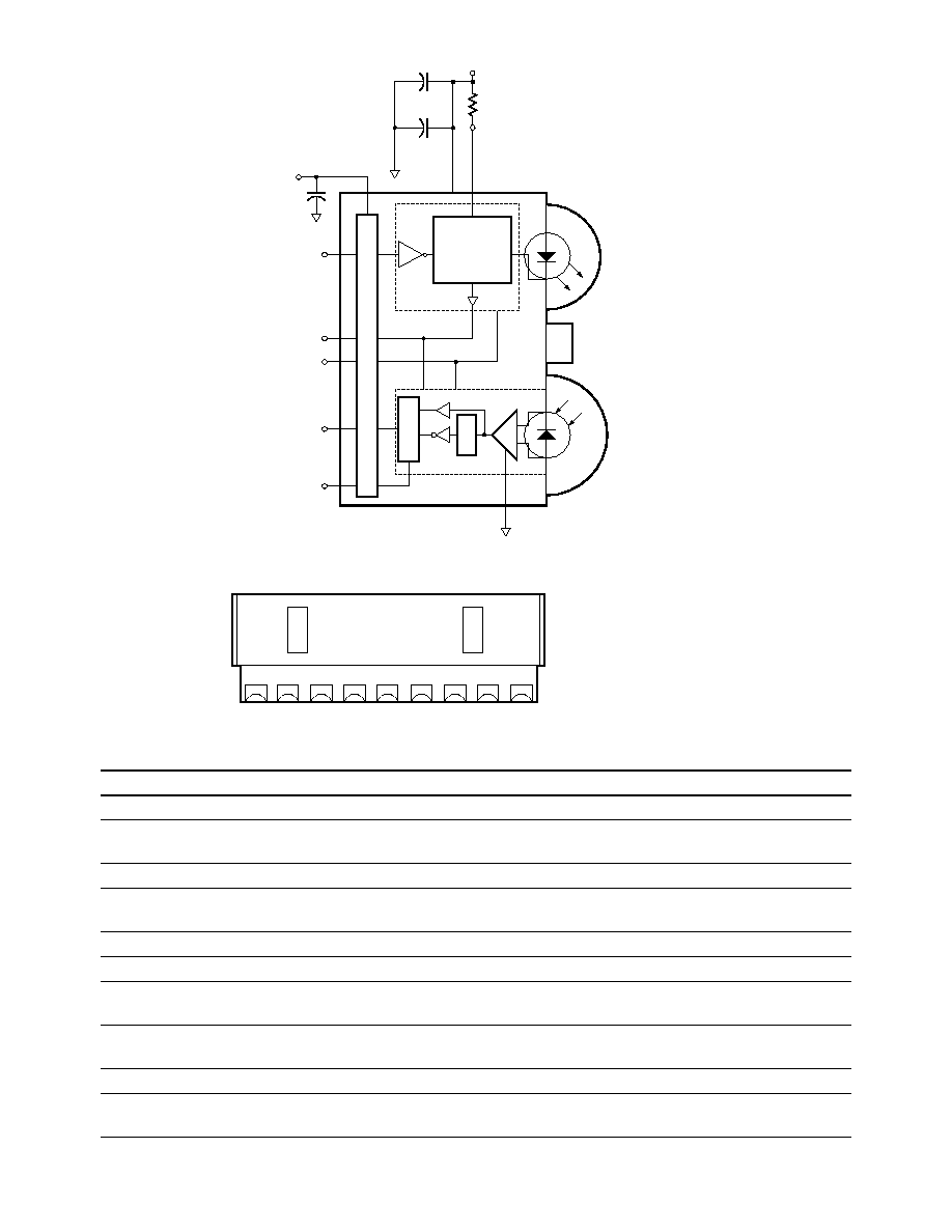
Functional Block Diagram
I/O Pins Configuration Table
Pin Symbol
Description
Note
1
GND
Ground
Connect to system ground.
2
I/OV
CC
Input/Output ASIC V
CC
Connect to ASIC logic controller V
CC
voltage or supply voltage. The voltage
at this pin must be equal to or less than supply voltage.
3
V
CC
Supply Voltage
Regulated 2.7 to 5.5 volts.
4
MIR_SEL
MIR Select
This pin to be driven high to select MIR mode and low for SIR mode.
Do not float this pin.
5
MD0
Mode 0
This pin must be driven either high or low. Do not float this pin.
6
MD1
Mode 1
This pin must be driven either high or low. Do not float the pin.
7
RXD
Receiver Data Output.
Output is a low pulse response when a light pulse is seen.
Active Low.
Active low.
8
TXD
Transmitter Data Input. Logic high turns the LED on. If held high longer than ~ 50
Á
s, the LED is turned
Active High.
off. TXD must be either driven high or low. Do not float this pin.
9
LEDA
LED Anode
Tied to external resistor, R1, to regulated V
CC
from 2.7 to 5.5 volts.
¡
SHIELD
EMI Shield
Do not connect shield directly to ground pin; connect to system ground via a
low inductance trace.
Pinout
REAR VIEW
9
8
7
6
5
4
3
2
1
ADJUSTABLE
OPTICAL
POWER
SHIELD
TXD (8)
MD0 (5)
MD1 (6)
RXD (7)
MIR_SEL (4)
CX3
I/0 V
CC
(2)
GND (1)
CX2
V
CC
(3)
R1
LEDA (9)
HSDL-3310
CX1

3
Transceiver Control Truth Table
MD0
MD1
MIR_SEL
RXD
TXD
1
0
X
Shutdown
Shutdown
0
0
0
SIR
Full Distance Power
0
1
0
SIR
50 cm Distance Power
1
1
0
SIR
30 cm Distance Power
0
0
1
MIR
Full Distance Power
0
1
1
MIR
50 cm Distance Power
1
1
1
MIR
30 cm Distance Power
X = Don't care
Transceiver I/O Truth Table
Inputs
Outputs
Transceiver Mode
MIR_SEL
TXD
EI
IE (LED)
RXD
Active
X
V
IH
X
High (On)
NV
Active
0
V
IL
EI
H
[1]
Low (Off)
Low
[3]
Active
1
V
IL
EI
H
[2]
Low (Off)
Low
[3]
Active
X
V
IL
EI
L
Low (Off)
High
Shutdown
X
X
[4]
Low (Off)
Low (Off)
NV
[5]
Notes:
1. In-Band EI
115.2 kb/s and MIR_SEL=0
2. In-Band EI
0.576 Mb/s and MIR_SEL=1
3. Logic low is a pulsed response.
4. To maintain low shutdown current, TXD needs to be driven high or low and not to be left floating.
5. RXD is internally pull-up to V
CC
through high impedance PMOS transistor (equivalent impedance is greater than 300 k
).
Recommended Application Circuit Components
Component
Recommended Value
R1
2.2
▒
5%, 0.5 Watt, for 2.7
V
CC
3.3 V operation
2.7
▒
5%, 0.5 Watt, for 3.0
V
CC
3.6 V operation
5.6
▒
5%, 0.5 Watt, for 4.5
V
CC
5.5 V operation
CX1
[1]
, CX3
0.47
Á
F
▒
20%, X7R Ceramic
CX2
[2]
6.8
Á
F
▒
20%, Tantalum
Caution: The component is susceptibile to damage from electrostatic discharge. It is advised that
normal static precautions be taken during handling and assembling of this component to prevent
damage and/or degradation, which may be caused by ESD.
X = Don't care
NV = Not valid
EI = In-Band infrared intensity at detector
Notes:
1. CX1 must be placed within 0.7 cm from HSDL-3310 for optimum noise immunity.
2. When using with noisy power supplies, supply rejection can be enhanced by including CX2 as
shown in "HSDL-3310 Functional Block Diagram."

4
Recommended Operating Conditions
Parameter
Symbol
Min.
Max.
Units
Conditions
Operating Temperature
T
A
¡20
70
░
C
Supply Voltage
V
CC
2.7
5.5
V
Input/Output Voltage
I/OV
CC
1.8
5.5
V
Logic Input Voltage Logic High
V
IH
2/3 IOV
CC
IOV
CC
V
Logic Low
V
IL
0
1/3 IOV
CC
V
Receiver Input
Irradiance
Logic High
EI
H
0.0036
500
mW/cm
2
For in-band signals
115.2 kb/s
[1]
0.0090
500
mW/cm
2
0.576 Mb/s
in-band signals
1.152 Mb/s
[1]
Logic Low
EI
L
0.3
Á
W/cm
2
For in-band signals
LED (Logic High) Current
I
LEDA
400
600
mA
V
LED
= V
CC
= 3.0, V
I
(TXD)
V
IH
Pulse Amplitude
MD0 = 0, MD1 = 0
Receiver Data Rate
0.0024
1.152
Mb/s
Ambient Light
See IrDA Serial Infrared Physical
Layer Link Specification,
Appendix A for ambient levels
Absolute Maximum Ratings
For implementations where case to ambient thermal resistance is
50
░
C/W.
Parameter
Symbol
Min.
Max.
Units
Storage Temperature
T
S
¡40
100
░
C
Operating Temperature
T
A
¡20
70
░
C
LED Supply Voltage
V
LED
0
7
V
Supply Voltage
V
CC
0
7
V
Input/Output Voltage
I/OV
CC
0
7
V
Input Voltage: TXD, MD0, MD1
V
I
0
7
V
Output Voltage: RXD
V
O
¡0.5
7
V
for TXD, MD0,
MD1,MIR_SEL

5
Electrical & Optical Specifications
Specifications (Min. and Max. values) hold over the recommended operating conditions unless otherwise noted.
Unspecified test conditions may be within the operating range. All typical values (Typ.) are at 25
░
C with V
CC
and IOV
CC
set to 3.0 V unless otherwise noted.
Parameter
Symbol
Min.
Typ.
Max.
Units
Conditions
Receiver
Viewing Angle
2
1/2
30
░
Peak Sensitivity
p
880
nm
Wavelength
RXD Output Voltage
Logic High
V
OH
IOV
CC
¡0.2
IOV
CC
V
I
OH
= ¡200
Á
A, EI
0.3
Á
W/cm
2
Logic Low
V
OL
0
0.4
V
I
OL
= 200
Á
A
RXD Pulse Width (SIR)
[2]
t
RPW
(SIR)
1
7.5
Á
s
1/2
15
░
, C
L
= 9 pF
RXD Pulse Width (MIR)
[3]
t
RPW
(MIR) 200
750
ns
1/2
15
░
, C
L
= 9 pF
RXD Rise and Fall Times
t
r
, t
f
25
100
ns
C
L
= 9 pF
Receiver Latency Time
[4]
t
L
25
50
Á
s
Receiver Wake Up Time
[5]
t
RW
18
100
Á
s
EI = 10 mW/cm
2
Transmitter
Radiant Intensity
IE
H
100
220
mW/sr
I
LEDA
= 400 mA,
1/2
15
░
,
TXD
V
IH
. MD0 = 0, MD1 = 0,
T
A
= 25
░
C
Viewing Angle
2
1/2
30
60
░
Peak Wavelength
p
875
nm
Spectral Line Half Width
1/2
35
nm
TXD Logic Levels
High
V
IH
2/3 IOV
CC
IOV
CC
V
Low
V
IL
0
1/3 IOV
CC
V
TXD Input Current
High
I
H
0.02
1
Á
A
V
I
V
IH
Low
I
L
¡1
¡0.02
1
Á
A
0
V
I
V
IL
LED Current
Off
I
VLED
0.03
1
Á
A
V
VLED
= V
CC
= 3.0 V, V
I
(TXD)
V
IL
MD0 = 0, MD1 = 0
Wakeup Time
[6]
t
TW
30
100
Á
s
Maximum Optical
t
PW(Max)
25
50
Á
s
Pulse Width
[7]
TXD Rise and
t
r
, t
f
40
ns
t
PW
(TXD) = 217 ns at 1.152 Mb/s
Fall Time (Optical)
TXD Pulse Width (SIR)
t
TPW
(SIR)
1.5
1.6
1.8
Á
s
t
PW
(TXD) = 1.6
Á
s at 115.2 kb/s
TXD Pulse Width (MIR)
t
TPW
(MIR) 148
217
260
ns
t
PW
(TXD) = 217 ns at 1.152 Mb/s