
Features
·
Ultra Small Surface Mount
Package
·
Minimal Height: 2.5 mm
·
V
cc
from 2.7 to 3.6 Volts
·
Withstands > 250 mV
p-p
Power Supply Ripple
·
LED Supply Voltage can
Range from 2.7 to 6.0 Volts
·
Low Shutdown Current
20 nA Typical
IrDA Data 1.2 Low Power
Compliant 115.2 kb/s Infrared
Transceiver
Technical Data
HSDL-3201
·
Complete Shutdown
TxD, RxD, PIN Diode
·
One Optional External
Component
·
Temperature Range:
-25
°
C to 85
°
C
·
32 mA LED Drive Current
·
Integrated EMI Shield
·
IEC825-1 Class 1 Eye Safe
·
Edge Detection Input
Prevents the LED from
Long Turn on Time
IrDA 1.2
LOW POWER
IrDA 1.0/1.2
STANDARD OR
LOW POWER
30° ILLUMINATION CONE
CELL PHONES
PAGERS
PDAs
CAMERAS
CELL PHONES
PAGERS
PRINTERS
PCs
PDAs
CAMERAS
20 CM TO LOW POWER DEVICES
30 CM TO STANDARD DEVICES
2
Applications
·
Mobile Telecom
Cellular Phones
Pagers
Smart Phones
·
Data Communication
PDAs
Portable Printers
·
Digital Imaging
Digital Cameras
Photo-Imaging Printers
Description
The HSDL-3201 is one of a new
generation of low-cost Infrared
(IR) transceiver modules from
Agilent Technologies. It features
the smallest footprint in the
industry at 2.5 H x 8.0 W x 3.0 D
mm. Although the supply voltage
can range from 2.7 V to 3.6 V,
the LED drive current is
internally compensated to a
constant 32 mA to assure that
link distances meet the IrDA Data
1.2 (low power) physical layer
specifications.
The HSDL-3201 meets the 20 cm
link distance to other IrDA 1.2
low power devices, and a 30 cm
link distance to IrDA 1.2 standard
devices.
I/O Pins Configuration Table
Pin
Symbol
Description
Notes
1
GND
Ground
Connect to system ground.
2
NC
No Connection
This pin must be left
unconnected.
3
V
CC
Supply Voltage
Regulated: 2.7 to 3.6 Volts
4
AGND
Analog Ground
Connect to a "quiet"
ground.
5
SD
Shut Down
This pin must be driven
Active High
either high or low. Do NOT
float the pin.
6
RXD
Receiver Data
Output is a low pulse for
Output. Active Low.
2.4
µ
s when a light pulse
is seen.
7
TXD
Transmitter Data
Logic high turns the LED
Input. Active High.
on. If held high longer than
~ 20
µ
s, the LED is turned
off. TXD must be driven
high or low. Do NOT float
the pin.
8
VLED
LED Voltage
May be unregulated: 2.7 to
6.0 volts.
-
SHIELD
EMI Shield
Connect to system ground
via a low inductance trace.
For best performance, do
not directly connect to
GND or AGND at the part.
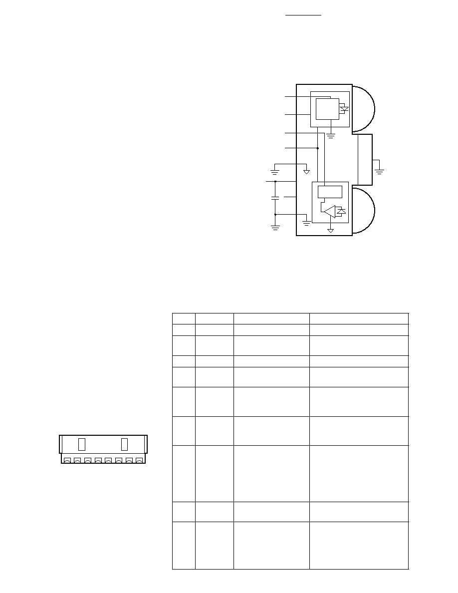
Application Circuit
Pinout, Rear View
VLED
TXD
7
LED
CURRENT
SOURCE
RXD
6
SHUT DOWN
5
RX PULSE
SHAPER
TXD
8 VLED
4 AGND
SD
RXD
V
CC
3
V
CC
2
NC
1 GND
C1
1.0 µF
SHIELD
8
7
6
5
4
3
2
1
3
Recommended Application Circuit Components
Component
Recommended Value
Note
C1
1.0
µ
F
1
Absolute Maximum Ratings
For implementations where case to ambient thermal resistance is
50
°
C/W.
Parameter
Symbol
Min.
Max.
Units
Storage Temperature
T
S
-40
100
°
C
Operating Temperature
T
A
-25
85
°
C
LED Supply Voltage
V
VLED
-0.5
7
V
Supply Voltage
V
CC
-0.5
7
V
Input Voltage: TXD, SD
V
I
0
V
CC
+
0.5
V
Output Voltage: RXD
V
O
-0.5
V
CC
+
0.5
V
Solder Reflow
See Reflow Profile, page 13
Temperature Profile
Transceiver I/O Truth
Table
The LED and RXD outputs are
controlled by the combination of
the TXD and SD pins and light
falling on the receiver. As shown
in the table below, the transmitter
is non-inverting; the LED is on
when the TXD pin is high and off
when TXD is low. The receiver is
inverting; the RXD pin is low
during IrDA signal pulses and
high when the receiver does not
see any light. When shutdown
(SD pin high), the LED is off (the
state of the TXD pin does not
matter), and the RXD pin is
pulled high with a weak internal
pullup.
SD
TXD
LED
Receiver
RXD
Notes
High
On
Don't care
Not Valid
2, 3
Low
Low
Off
IrDA Signal
Low
4, 5
No Signal
High
High
Don't care
Off
Don't care
High
6
Shutdown Mode Notes
When the HSDL-3201 is in
Shutdown Mode (SD pin high),
the part presents different
impedances to the rest of the
circuit than when it is in normal
mode.
RXD Pin: This pin is NOT Tri-
state. During shutdown the
equivalent circuit is a weak
pullup (~300 k
) to V
cc
. The
ESD protection diodes to V
cc
and
Ground are also present.
TXD Pin: Input protection
diodes are present.
VLED Pin: Possible leakage
current of 1.5 nA.
SD Pin: Will draw approximately
16 nA when driven high.
Marking Information
The unit is marked with the
letters "HPL" and the datecode
"YWW" on the shield. Y is the last
digit of the year, and WW is the
workweek.
Ordering Information
Specify the part number followed
by an option number.
HSDL-3201#XXX
There are three options available:
011
Taped in a short strip (no
reel), 10 per strip
001
Taped and 7" Reel
Packaging, 500 per reel
021
Taped and 13" Reel
Packaging, 2500 per reel
Caution: The BiCMOS inherent to this design of this component increases the component's
susceptibility to damage from electrostatic discharge (ESD). It is advised that normal static
precautions be taken in handling and assembly of this component to prevent damage and/or
degradation which may be induced by ESD.

4
Recommended Operating Conditions
Parameter
Symbol
Min.
Max.
Units
Conditions
Notes
Operating Temperature
T
A
-25
85
°
C
Supply Voltage
V
CC
2.7
3.6
V
LED Supply Voltage
V
LED
2.7
6.0
V
TXD, SD Input
Logic High
V
IH
2/3 V
CC
V
CC
V
Voltage
Logic Low
V
IL
0
1/3 V
CC
V
Receiver Input
Logic High
EI
H
0.0081
500
mW/cm
2
For in-band signals.
7
Irradiance
Logic Low
EI
L
0.3
µ
W/cm
2
For in-band signals.
7
Receiver Data Rate
2.4
115.2
kb/s
Ambient Light
See Test Methods on page 16 for details
RXD Output Waveform
LED Optical Waveform
TXD "Stuck ON" Protection
Receiver Wakeup Time Definition
Transmitter Wakeup Time Definition
tf
VOH
90%
50%
10%
VOL
tpw
tr
tf
LED OFF
90%
50%
10%
LED ON
tpw
tr
tpw (MAX.)
TXD
LED
RX
LIGHT
tRW
RXD
SD
TX
LIGHT
tTW
TXD
SD

5
Electrical & Optical Specifications
Specifications hold over the recommended operating conditions unless otherwise noted. Unspecified test
conditions may be anywhere in their operating range. All typical values are at 25
°
C and 3.0 V unless
otherwise noted.
Parameter
Symbol
Min.
Typ.
Max.
Units
Conditions
Note
Receiver
Viewing Angle
2
1/2
30
°
Peak Sensitivity
p
880
nm
Wavelength
RXD Output
Logic High
V
OH
V
CC
-0.2
V
CC
V
I
OH
=-200
µ
A, EI
0.3
µ
W/cm
2
Voltage
Logic Low
V
OL
0
0.4
V
I
OL
=200
µ
A
8
RXD Pulse Width
t
PW
2.0
2.45
3.0
µ
s
8
RXD Rise Time
t
R
11
20
ns
t
PW
(EI)=1.6
µ
s, C
L
=10 pF
RXD Fall Time
t
F
16
25
ns
t
PW
(EI)=1.6
µ
s, C
L
=10 pF
Receiver Latency Time
t
L
25
50
µ
s
9
Receiver Wake Up Time
t
RW
28
40
µ
s
10
Transmitter
Radiant Intensity
EI
H
4
9
28.8
mW/Sr
T
A
=25
°
C,
1/2
15
°
, TXD
2/3 V
CC
Viewing Angle
2
1/2
30
60
°
Peak Wavelength
p
875
nm
Spectral Line Half Width
1/2
35
nm
Optical Pulse Width
t
OPW
1.41
1.6
2.23
µ
s
t
PW
(TXD)=1.6
µ
s
Max. Optical Pulse Width
t
OPWM
20
30
µ
s
TXD pin stuck high
Optical Rise Time
t
OR
180
600
ns
t
PW
(TXD)=1.6
µ
s
Optical Fall Time
t
OF
180
600
ns
t
PW
(TXD)=1.6
µ
s
TXD Logic
High
V
IH
2/3 V
CC
V
CC
V
Levels
Low
V
IL
0
1/3 V
CC
V
TXD Input
High
I
H
25
nA
V
I
2/3 V
CC
Current
Low
I
L
-15
nA
0
V
I
1/3 V
CC
LED
On
I
VLED
32
mA
V
VLED
=V
CC
=3.6 V, V
I
(TXD)
2/3 V
CC
Current
Off
I
VLED
1.5
nA
V
VLED
=V
CC
=3.6 V, V
I
(TXD)
1/3 V
CC
Shutdown
I
VLED
1.5
nA
V
I
(SD)
2/3 V
CC
Transmitter Wake Up Time
t
TW
12
20
µ
s
11
Transceiver
SD Logic
High
V
IH
2/3 V
CC
V
CC
V
Levels
Low
V
IL
0
1/3 V
CC
V
SD Input
High
I
H
16
nA
V
I
2/3 V
CC
Current
Low
I
L
-150
nA
0
V
I
1/3 V
CC
DC Supply
Shutdown
I
CC1
20
200
nA
V
CC
=3.6 V,V
SD
V
CC
- 0.5, T
A
=25
°
C
Current
Idle
I
CC2
100
µ
A
V
CC
=3.6 V, V
I
(TXD)
1/3 V
CC
, EI=0
AC Supply
Active, receive
I
CC3
0.8
3.0
mA
V
CC
=3.6 V,
V
I
(TXD)
1/3 V
CC
12,13
Current
Active,
I
CC4
9.0
mA
V
CC
=3.6 V,
V
I
(TXD)
2/3 V
CC
14
transmit
Notes at top of next page.