Document Outline
- Selection Guide
- Technical Data
- List of Figures
3-84
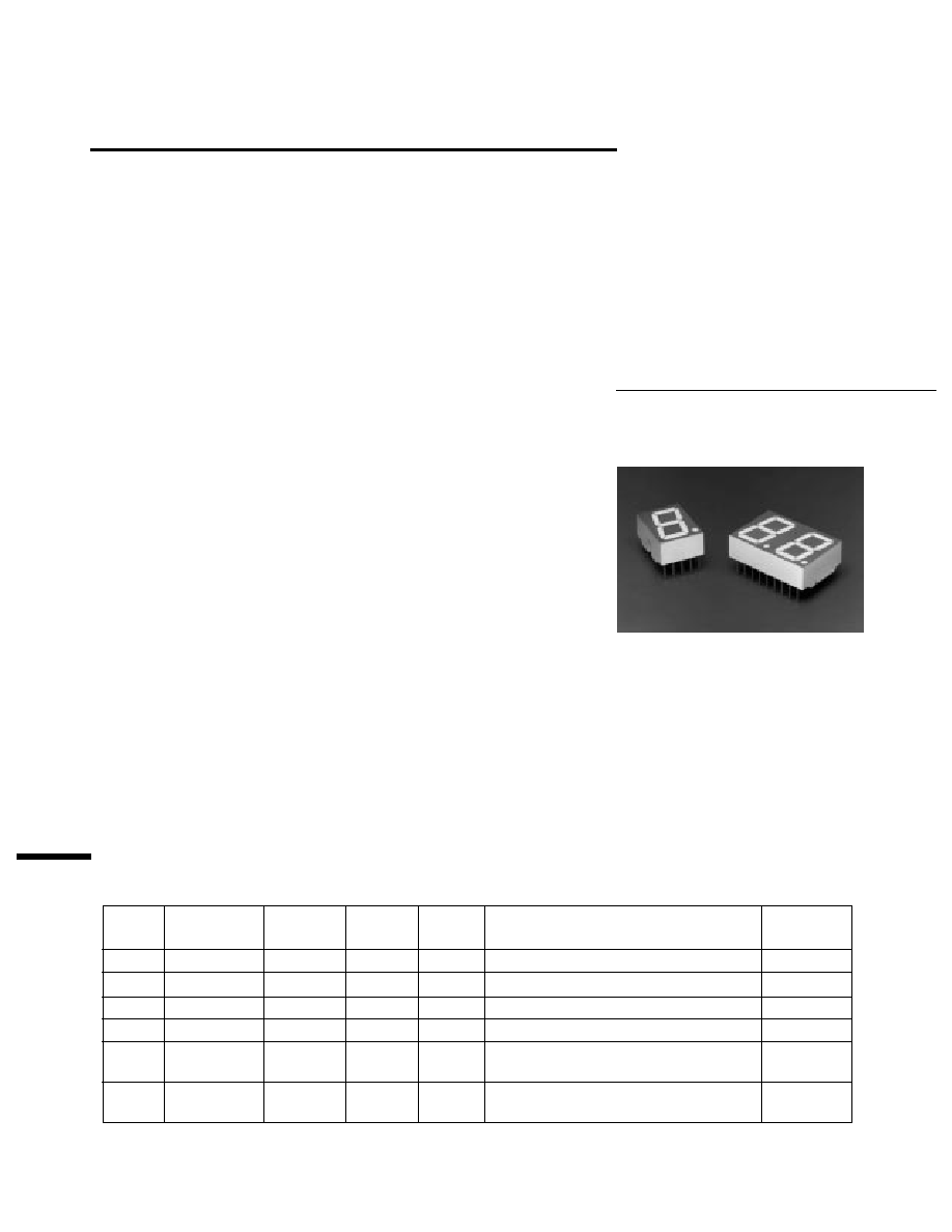
14.2 mm (0.56 inch)
Seven Segment Displays
Technical Data
Features
· Industry Standard Size
· Industry Standard Pinout
15.24 mm (0.6 in.) DIP Leads
on 2.54 mm (0.1 in.) Centers
· Choice of Colors
Red, AlGaAs Red, High
Efficiency Red, Yellow, Green
· Excellent Appearance
Evenly Lighted Segments
Mitered Corners on Segments
Gray Package Gives Optimum
Contrast
±
50
°
Viewing Angle
· Design Flexibility
Common Anode or Common
Cathode
Single and Dual Digits
Right Hand Decimal Point
±
1. Overflow Character
· Categorized for Luminous
Intensity
Yellow and Green Categorized
for Color
Use of Like Categories Yields a
Uniform Display
· High Light Output
· High Peak Current
· Excellent for Long Digit
String Multiplexing
· Intensity and Color
Selection Option
See Intensity and Color
Selected Displays Data Sheet
· Sunlight Viewable AlGaAs
Description
The 14.2 mm (0.56 inch) LED
seven segment displays are
designed for viewing distances up
to 7 metres (23 feet). These
devices use an industry standard
size package and pinout. Both the
numeric and
±
1 overflow devices
feature a right hand decimal
point. All devices are available as
either common anode or common
cathode.
Red
AlGaAs Red
HER
Yellow
Green
Package
HDSP-
HDSP-
[1]
HDSP-
[1]
HDSP-
HDSP-
Description
Drawing
5301
H151
5501
5701
5601
Common Anode Right Hand Decimal
A
5303
H153
5503
5703
5603
Common Cathode Right Hand Decimal
B
5307
H157
5507
5707
5607
Common Anode
±
1. Overflow
C
5308
H158
5508
5708
5608
Common Cathode
±
1. Overflow
D
5321
5521
5721
5621
Two Digit Common Anode Right Hand
E
Decimal
5323
5523
5723
5623
Two Digit Common Cathode Right Hand
F
Decimal
Devices
Note:
1. These displays are recommended for high ambient light operation. Please refer to the HDSP-H10X/K12X AlGaAs and HDSP-555X HER
data sheet for low current operation.
HDSP-530X Series
HDSP-532X Series
HDSP-550X Series
HDSP-552X Series
HDSP-560X Series
HDSP-562X Series
HDSP-570X Series
HDSP-572X Series
HDSP-H15X Series
H
5963-7388E

3-85
These displays are ideal for most
applications. Pin for pin
equivalent displays are also
available in a low current design.
The low current displays are ideal
FUNCTION
PIN
A
B
C
D
E
F
1
CATHODE e
ANODE e
CATHODE c
ANODE c
E CATHODE NO. 1
E ANODE NO. 1
2
CATHODE d
ANODE d
ANODE c, d
CATHODE c, d
D CATHODE NO. 1
D ANODE NO. 1
3
ANODE
[3]
CATHODE
[4]
CATHODE b
ANODE b
C CATHODE NO. 1
C ANODE NO. 1
4
CATHODE c
ANODE c
ANODE a, b, DP
CATHODE a, b, DP
DP CATHODE NO. 1
DP ANODE NO. 1
5
CATHODE DP
ANODE DP
CATHOPDE DP
ANODE DE
E CATHODE NO. 1
E ANODE NO. 2
6
CATHODE b
ANODE b
CATHODE a
ANODE a
D CATHODE NO. 2
D ANODE NO. 2
7
CATHODE a
ANODE a
ANODE a, b, DP
CATHODE a, b, DP
G CATHODE NO. 2
G ANODE NO. 2
8
ANODE
[3]
CATHODE
[4]
ANODE c, d
CATHODE c, d
C CATHODE NO. 2
C ANODE NO. 2
9
CATHODE f
ANODE f
CATHODE d
ANODE d
DP CATHODE NO. 2
DP ANODE NO. 2
10
CATHODE g
ANODE g
NO PIN
NO PIN
B CATHODE NO. 2
B ANODE NO. 2
11
A CATHODE NO. 2
A ANODE NO. 2
12
F CATHODE NO. 2
F ANODE NO. 2
13
DIGIT NO. 2 ANODE
DIGIT NO. 2 CATHODE
14
DIGIT NO. 1 ANODE
DIGIT NO. 1 CATHODE
15
B CATHODE NO. 1
B ANODE NO. 1
16
A CATHODE NO. 1
A ANODE NO. 1
17
G CATHODE NO. 1
G ANODE NO. 1
18
F CATHODE NO. 1
F ANODE NO. 1
NOTES:
1. ALL DIMENSIONS IN MILLIMETRES (INCHES).
2. ALL UNTOLERANCED DIMENSIONS ARE FOR REFERENCE ONLY.
3. REDUNDANT ANODES.
4. REDUNDANT CATHODES.
5. FOR HDSP-5600/-5700 SERIES PRODUCT ONLY.
for portable applications. For
additional information see the
Low Current Seven Segment
Displays data sheet.
Package Dimensions

3-86
Internal Circuit Diagram
Notes:
1. See Figure 1 to establish pulsed conditions.
2. Derate above 80
°
C at 0.63 mA/
°
C.
3. See Figure 2 to establish pulsed conditions.
4. Derate above 46
°
C at 0.54 mA/
°
C.
5. See Figure 7 to establish pulsed conditions.
6. Derate above 53
°
C at 0.45 mA/
°
C.
Red
AlGaAs Red
HER
Yellow
Green
HDSP-5300
HDSP-H150
HDSP-5500
HDSP-5700
HDSP-5600
Description
Series
Series
Series
Series
Series
Units
Average Power per Segment or DP
82
96
105
80
105
mW
Peak Forward Current per
150
[1]
160
[3]
90
[5]
60
[7]
90
[9]
mA
Segment or DP
DC Forward Current per
25
[2]
40
[4]
30
[6]
20
[8]
30
10]
mA
Segment or DP
Operating Temperature Range
-40 to +100
-20 to +100
[11]
-40 to +100
°
C
Storage Temperature Range
-55 to +100
°
C
Reverse Voltage per
3.0
V
Segment or DP
Lead Solder Temperature for
3 Seconds (1.60 mm [0.063 in.]
260
°
C
below seating plane)
Absolute Maximum Ratings
7. See Figure 8 to establish pulsed conditions.
8. Derate above 81
°
C at 0.52 mA/
°
C.
9. See Figure 9 to establish pulsed conditions.
10. Derate above 39
°
C at 0.37 mA/
°
C.
11. For operation below -20
°
C, contact your local HP
components sales office or an authorized distributor.
3-87
Electrical/Optical Characteristics at T
A
= 25
°
C
Red
Device
Series
HDSP-
Parameter
Symbol
Min.
Typ.
Max.
Units
Test Conditions
600
1300
I
F
= 20 mA
Luminous Intensity/Segment
[1,2]
I
V
µ
cd
(Digit Average)
1400
I
F
= 100 mA Peak:
1 of 5 df
Forward Voltage/Segment or DP
V
F
1.6
2.0
V
I
F
= 20 mA
53XX
Peak Wavelength
PEAK
655
nm
Dominant Wavelength
[3]
d
640
nm
Reverse Voltage/Segment or DP
[4]
V
R
3.0
12
V
I
R
= 100
µ
A
Temperature Coefficient of
V
F
/
°
C
-2
mV/
°
C
V
F
/Segment or DP
Thermal Resistance LED Junction-
R
J-Pin
345
°
C/W/
to-Pin
Seg
Device
Series
HDSP-
Parameter
Symbol
Min.
Typ.
Max.
Units
Test Conditions
Luminous Intensity/Segment
[1,2,5]
I
V
9.1
16.0
mcd
I
F
= 20 mA
(Digit Average)
1.8
I
F
= 20 mA
Forward Voltage/Segment or DP
V
F
V
2.0
3.0
I
F
= 100 mA
H15X
Peak Wavelength
PEAK
645
nm
Dominant Wavelength
[3]
d
637
nm
Reverse Voltage/Segment or DP
[4]
V
R
3.0
15
V
I
R
= 100
µ
A
Temperature Coefficient of
V
F
/
°
C
-2
mV/
°
C
V
F
/Segment or DP
Thermal Resistance LED Junction-
R
J-Pin
400
°
C/W/
to-Pin
Seg
AlGaAs Red

3-88
Device
Series
HDSP-
Parameter
Symbol
Min.
Typ.
Max.
Units
Test Conditions
900
2800
I
F
= 10 mA
Luminous Intensity/Segment
[1,2,6]
I
V
µ
cd
(Digit Average)
3700
I
F
= 60 mA Peak:
1 of 6 df
Forward Voltage/Segment or DP
V
F
2.1
2.5
V
I
F
= 20 mA
55XX
Peak Wavelength
PEAK
635
nm
Dominant Wavelength
[3]
d
626
nm
Reverse Voltage/Segment or DP
[4]
V
R
3.0
30
V
I
R
= 100
µ
A
Temperature Coefficient of
V
F
/
°
C
-2
mV/
°
C
V
F
/Segment or DP
Thermal Resistance LED Junction-
R
J-Pin
345
°
C/W/
to-Pin
Seg
High Efficiency Red
Device
Series
HDSP-
Parameter
Symbol
Min.
Typ.
Max.
Units
Test Conditions
600
1800
I
F
= 10 mA
Luminous Intensity/Segment
[1,2]
I
V
µ
cd
(Digit Average)
2750
I
F
= 60 mA Peak:
1 of 6 df
Forward Voltage/Segment or DP
V
F
2.1
2.5
V
I
F
= 20 mA
57XX
Peak Wavelength
PEAK
583
nm
Dominant Wavelength
[3,7]
d
581.5
586
592.5
nm
Reverse Voltage/Segment or DP
[4]
V
R
3.0
40
V
I
R
= 100
µ
A
Temperature Coefficient of
V
F
/
°
C
-2
mV/
°
C
V
F
/Segment or DP
Thermal Resistance LED Junction-
R
J-Pin
345
°
C/W/
to-Pin
Seg
Yellow