Document Outline
- HDMP-0482
- Description
- Features
- Applications
- Block Diagram
- CDR
- DV Output
- AV Output
- BLL Output
- EQU Input
- BYPASS[N]- Input
- REFCLK Input
- RFCM Input
- MODE_VDD Input
- Pin Connection Diagram
- Package Layout and Marking
- I/O Type Definitions
- Pin Definitions
- Absolute Maximum Ratings
- Guaranteed Operating Rates
- Reference Clock Requirements
- Electrical Specifications
- Power Dissipation
- Output Jitter Characteristics
- Locking Characteristics
- Eye Diagram
- Setup for Measurement of Random Jitter
- Setup for Measurement of Deterministic Jitter
- Simplified Circuit Schematic
- Package Information
- Thermal Characteristics
- Package Drawing
- Recommended Power Supply Filtering
Agilent HDMP-0482
Octal Cell Port Bypass Circuit
with CDR and Data Valid Detection
Data Sheet
Description
The HDMP-0482 is an Octal Cell
Port Bypass Circuit (PBC) with
Clock and Data Recovery (CDR)
and data valid detection capabil-
ity included. This device mini-
mizes part count, cost and jitter
accumulation while repeating
incoming signals. Port Bypass
Circuits are used in hard disk
arrays constructed in Fibre
Channel Arbitrated Loop
(FC-AL) configurations. By using
Port Bypass Circuits, hard disks
may be pulled out or swapped
while other disks in the array are
available to the system.
A Port Bypass Circuit (PBC)
consists of multiple 2:1 multiplex-
ers daisy chained along with a
CDR. Each port has two modes of
operation: "disk in loop" and
"disk bypassed". When the "disk
in loop" mode is selected, the loop
goes into and out of the disk drive
at that port. For example, data
goes from the HDMP-0482's
TO_NODE[n]
± differential output
pins to the Disk Drive Transceiver
IC's (e.g. an HDMP-1636A) Rx
±
differential input pins. Data from
the Disk Drive Transceiver IC's
Tx
± differential outputs goes to
Features
· Supports 1.0625 GBd fibre channel
operation
· Supports 1.25 GBd Gigabit Ethernet
(GE) operation
· Octal cell PBC/CDR in one package
· CDR location determined by choice
of cable input/output
· Amplitude valid detection on
FM_NODE[7] input
· Data valid detection on
FM_NODE[0] input
Run length violation detection
Comma detection
Configurable for both single-
frame and multi-frame detection
· Equalizers on all inputs
· High speed LVPECL I/O
· Buffered Line Logic (BLL) outputs
(no external bias resistors
required)
· 1.09 W typical power at Vcc=3.3V
· 64 Pin, 14 mm, low cost plastic QFP
package
Applications
· RAID, JBOD, BTS cabinets
· Four 2:1 muxes
· Four 1:2 buffers
· 1 = > N gigabit serial buffer
· N = > 1 gigabit serial mux
the HDMP-0482's FM_NODE[n]
±
differential input pins. When the
"disk bypassed" mode is selected,
the disk drive is either absent or
non-functional and the loop
bypasses the hard disk.
The "disk bypassed" mode is
enabled by pulling the BYPASS[n]-
pin low. Leave BYPASS[n]-
floating to enable the "disk in
loop" mode. HDMP-0482's may be
cascaded with other members of
the HDMP-04XX/HDMP-05XX
family through the FM_NODE and
TO_NODE pins to accommodate
any number of hard disks. The
unused cells in this PBC may be
bypassed by using pulldown
resistors on the BYPASS[n]- pins
for these cells.
An HDMP-0482 may also be used
as eight 1:1 buffers, one with a
CDR and seven without. For
example, an HDMP-0482 may be
placed in front of a CMOS ASIC
to clean the jitter of the outgoing
signal (CDR path) and to better
read the incoming signal (non-
CDR path). In addition, the
HDMP-0482 may be configured as
four 2:1 multiplexers or as four
1:2 buffers.
HDMP-0482
CAUTION: As with all semiconductor ICs, it is advised that normal static precautions
be taken in the handling and assembly of this component to prevent damage and/or
degradation which may be induced by electrostatic discharge (ESD).

2
Figure 1. Block Diagram of HDMP-0482.
1
1
0
0
1
BYP
ASS1
2
1
0
BYP
ASS2
3
1
0
BYP
ASS3
4
1
0
BYP
ASS4
5
1
0
BYP
ASS5
6
1
0
BYP
ASS6
7
1
0
BYP
ASS7
0
1
0
FM_NODE(7)_A
V
BYPASS0
MODE_VDD
RFCM
REFCLK
FSEL
AV
BYPASS0
MODE_VDD
FM_NODE[0]_DV
CDR
DV
The HDMP-0482 design allows for
CDR placement at any location
with respect to the hard disk
slots. For example, if the BY-
PASS[0]- pin is floating and hard
disk slots A to G are connected to
PBC cells 1 to 7, respectively, the
CDR function will be performed
HDMP-0482 Block Diagram
CDR
The Clock and Data Recovery
(CDR) block is responsible for
frequency and phase locking onto
the incoming serial data stream
and resampling the incoming
data based on the recovered
clock. An automatic locking
feature allows the CDR to lock
onto the input data stream
without external training con-
trols. It does this by continually
frequency locking onto the
106.25 MHz reference clock
(REFCLK) and then phase
locking onto the input data
stream. Once bit locked, the CDR
generates a high-speed sampling
clock. This clock is used to
before entering the hard disk at
slot A. To obtain a CDR function
after slot G, BYPASS[1]- must be
floating and hard disk slots A to
G must be connected to PBC cells
2,3,4,5,6,7 and 0, respectively.
Table 1 shows all possible
connections.
For configurations where the CDR
is before slot A, a Data Valid
(FM_NODE[0]_DV) pin indicates
whether the incoming data on
FM_NODE[0]
± is valid Fibre
Channel data. In addition, an
Amplitude Valid (FM_NODE[7]AV)
pin shows the status of the signal
at FM_NODE[7].
sample or repeat the incoming
data to produce the CDR output.
The CDR jitter specifications
listed in this data sheet assume
an input that has been 8B/10B
encoded.
DV Output
The Data Valid (DV) block detects
if the incoming data on
FM_NODE[0]
± is valid Fibre
Channel data. The DV checks for
sufficient K28.5+ characters (per
Fibre Channel framing rules) and
for run length violations (per 8B/
10B encoding) on the data
coming out of the CDR. The
FM_NODE[0]_DV output is
pulled low if a run length viola-
tion (RLV) occurs, or if there are
no commas detected (NCD) in a
sufficient time. It is pulled high if
no errors are found. A RLV error
is defined as any consecutive
sequence of 1s or 0s greater than
five in the serial data bit stream.
A NCD error indicates the
absence of a seven-bit pattern
(0011111) present in the positive
disparity comma (K28.5+)
character. A K28.5+ character
should occur at the beginning of
every Fibre Channel frame of
2148 bytes (or 21480 serial bits),
as well as many times within and
between frames. If this seven-bit
pattern is not found within a 2
15
bit (~31 µs) interval, an NCD
error is generated.

3
When the DV is configured in
single-frame mode (FSEL low),
any RLV and NCD errors stored
during this 2
15
bit interval cause
FM_NODE[0]_DV to be pulled
low on the next subsequent
interval. FM_NODE[0]_DV
remains low until after an entire
2
15
bit interval in which no RLVs
occur and at least one comma is
detected. At that time,
FM_NODE[0]_DV is pulled high.
A multi-frame mode (FSEL high)
configuration of the DV is also
available. When in multi-frame
mode, the FM_NODE[0]_DV
output is only pulled low when
four consecutive 2
15
bit intervals
of bad data have been transmit-
ted. Once low, FM_NODE[0]_DV
does not go high again until four
consecutive 2
15
bit intervals of
good data are transmitted.
AV Output
The Amplitude Valid (AV) block
detects if the incoming data on
FM_NODE[7]
± is valid by exam-
ining the differential amplitude
of that input. The incoming data
is considered valid, and
FM_NODE[7]_AV is driven high,
as long as the amplitude is
greater than 400 mV (differential
peak-to-peak). FM_NODE[7]_AV
is driven low as long as the
amplitude of the input signal is
less than 100 mV (differential
peak-to-peak). When the ampli-
tude of the input signal is be-
tween 100 400 mV (differential
peak-to-peak), FM_NODE[7]_AV
is unpredictable. The
FM_NODE[7]_AV output is
latched in with an internally
generated 2
15
bit clock. Similar to
the DV function, the AV can be
configured for single-frame or
multi-frame operation.
BLL Output
All TO_NODE[n]
± high-speed
differential outputs are driven by
a Buffered Line Logic (BLL)
circuit that has on-chip source
termination, so no external bias
resistors are required. The BLL
Outputs on the HDMP-0482 are of
equal strength and can drive in
excess of 120 inches of FR-4 PCB
trace. Unused outputs should not
be left unconnected. Ideally,
unused outputs should have their
differential pins shorted together
with a short PCB trace. If trans-
mission lines are connected to
the output pins, the lines should
be differentially terminated with
an appropriate resistor. The value
of the termination resistor should
match the PCB trace differential
impedance.
EQU Input
All FM_NODE[n]
± high-speed
differential inputs have an
Equalization (EQU) buffer to
offset the effects of skin loss and
dispersion on PCBs. An external
termination resistor is required
across all high-speed inputs.
BYPASS[N]- Input
The active low BYPASS[n]- inputs
control the data flow through the
HDMP-0482. All BYPASS pins are
LVTTL and contain internal pull-
up circuitry. To bypass a port,
the appropriate BYPASS[n]- pin
should be connected to GND
through a 1k
resistor. Other-
wise, the BYPASS[n]- inputs
should be left to float. In this
case, the internal pull-up cir-
cuitry will force them high.
REFCLK Input
The LVTTL REFCLK input
provides a reference oscillator
for frequency acquisition of the
CDR. The REFCLK frequency
should be within
±100 ppm of
one-tenth or one-twentieth of the
incoming data rate in baud
(106.25 MHz
±100 ppm, or
53.125 MHz
±100 ppm for FC-AL
running at 1.0625 GBd).
RFCM Input
The LVTTL RFCM input config-
ures the CDR to accept a
REFCLK at either one-tenth or
one-twentieth of the incoming
data rate in baud. The RFCM
input has internal pull-up
circuitry, so the user should
connect the pin to GND through
a 1k
resistor for a REFCLK at
one-twentieth the incoming data
rate. For a REFCLK at one-tenth
the incoming data rate, let RFCM
float high.
MODE_VDD Input
The active high valid data detect
mode pin selects data checking of
the FM_NODE [0] +/- inputs.
When high, MODE_VDD overides
BYPASS [0] and forces the
incoming data into the CDR for
error checking. When low, the
chip can be configured for CDR
anywhere capability. Refer to
Figures 2 & 3 for high and low
MODE_VDD configuration.

4
Figure 2. Block Diagram of HDMP-0482, MODE_VDD is HIGH.
1
1
0
0
1
BYP
ASS1
2
1
0
BYP
ASS2
3
1
0
BYP
ASS3
4
1
0
BYP
ASS4
5
1
0
BYP
ASS5
6
1
0
BYP
ASS6
7
1
0
BYP
ASS7
0
FM_NODE(7)_A
V
AV
BYPASS0
FM_NODE[0]_DV
CDR
DV
Figure 3. Block Diagram of HDMP-0482, MODE_VDD is LOW.
1
1
0
BYP
ASS1
2
1
0
BYP
ASS2
3
1
0
BYP
ASS3
4
1
0
BYP
ASS4
5
1
0
BYP
ASS5
6
1
0
BYP
ASS6
7
1
0
1
0
BYP
ASS7
0
FM_NODE(7)_A
V
AV
BYP
ASS0
FM_NODE[0]_DV
CDR
DV
5
Table 1. Pin Connection Diagram to Achieve Desired CDR Location.
Hard Disk
A B C D E F G
A B C D E F G
A B C D E F G
A B C D E F G
Connection to PBC Cell
1 2 3 4 5 6 7
0 1 2 3 4 5 6 7
0 1 2 3 4 5 6 7
0 1 2 3 4
CDR Position (x)
xA B C D E F G
AxB C D E F G
A BxC D E F G
A B CxD E F G
Cell Connection to Cable
0
7
6
5
Hard Disk
A B C D E F G
A B C D E F G
A B C D E F G
A B C D E F G
Connection to PBC Cell
5 6 7 0 1 2 3
4 5 6 7 0 1 2
3 4 5 6 7 0 1
2 3 4 5 6 7 0
CDR Position (x)
A B C DxE F G
A B C D ExF G
A B C D E FxG
A B C D E F Gx
Cell Connection to Cable
4
3
2
1
x denotes CDR position with respect to hard disks.
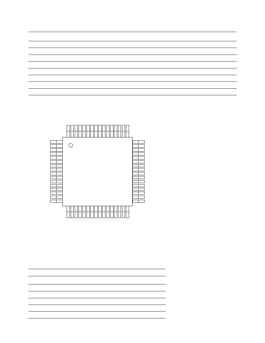
Figure 4. HDMP-0482 Package Layout and Marking, Top View.
nnnn-nnn = wafer lot - build number; Rz.zz = Die Revision; S = Supplier Code; YYWW = Date Code
(YY = year, WW = work week); COUNTRY = country of manufacture (on back side).
BYPASS[7]-
REFCLK
RFCM
FM_NODE[0]_DV
VCC
GND
MODE_VDD
VCCA
GND
CPLL1
CPLL0
FSEL
BYPASS[0]-
FM_NODE[7]_AV
FM_NODE[0]-
FM_NODE[0]+
48
47
46
45
44
43
42
41
40
39
38
37
36
35
34
33
1
2
3
4
5
6
7
8
9
10
11
12
13
14
15
16
64 63 62 61 60 59 58 57 56 55 54 53 52 51 50 49
17 18 19 20 21 22 23 24 25 26 27 28 29 30 31 32
VCCHS
TO_NODE[5]+
TO_NODE[5]-
VCCHS
TO_NODE[4]+
TO_NODE[4]-
BYPASS[4]-
FM_NODE[4]+
FM_NODE[4]-
GND
FM_NODE[3]+
FM_NODE[3]-
BYPASS[3]-
TO_NODE[3]+
TO_NODE[3]-
VCCHS
TO_NODE[2]+
TO_NODE[2]-
BYPASS[2]-
FM_NODE[2]+
FM_NODE[2]-
VCC
FM_NODE[1]+
FM_NODE[1]-
BYPASS[1]-
TO_NODE[1]+
TO_NODE[1]-
VCCHS
TO_NODE[0]+
TO_NODE[0]-
GND
VCC
VCC
FM_NODE[7]+
FM_NODE[7]-
GND
TO_NODE[7]+
TO_NODE[7]-
VCCHS
TO_NODE[6]+
TO_NODE[6]-
BYPASS[6]-
FM_NODE[6]+
FM_NODE[6]-
GND
FM_NODE[5]+
FM_NODE[5]-
BYPASS[5]-
HDMP-0482
nnnn-nnn Rz.zz
S YYWW
Agilent
Table 2. I/O Type Definitions.
I/O Type
Definition
I-LVTTL
LVTTL Input
O-LVTTL
LVTTL Output
HS_OUT
High Speed Output, LVPECL Compatible
HS_IN
High Speed Input
C
External circuit node
S
Power supply or ground