Ultra High CMR, Small Outline,
5 Lead, High Speed Optocoupler
Technical Data
HCPL-M454
Features
· Function Compatible with
HCPL-4504
· Surface Mountable
· Very Small, Low Profile
JEDEC Registered
Package Outline
· Compatible with Infrared
Vapor Phase Reflow and
Wave Soldering Processes
· Short Propagation Delays
for TTL and IPM
Applications
· Very High Common Mode
Transient Immunity:
Guaranteed 15 kV/
µ
s at
V
CM
= 1500 V
· High CTR: >25% at 25
°
C
· Guaranteed Specifications
for Common IPM
Applications
· TTL Compatible
· Guaranteed ac and dc
Performance Over
Temperature: 0
°
C to 70
°
C
· Open Collector Output
· Recognized Under the
Component Program of
U.L. (File No. E55361) for
Dielectric Withstand Proof
Test Voltage of 3750 Vac. 1
Minute
· Lead Free Option "-000E"
Applications
· Inverter Circuits and
Intelligent Power Module
(IPM) Interfacing - Shorter
propagation delays and
guaranteed (t
PLH
- t
PHL
)
specifications. (See Power
Inverter Dead Time section).
· High Speed Logic Ground
Isolation - TTL/TTL, TTL/
LTTL, TTL/CMOS, TTL/
LSTTL
· Line Receivers - High com-
mon mode transient immunity
(>15 kV/
µ
s for a TTL load/
drive) and low input-output
capacitance (0.6 pF).
· Replace Pulse Trans-
formers - Save board space
and weight
· Analog Signal Ground
Isolation - Integrated photon
detector provides improved
linearity over phototransistors
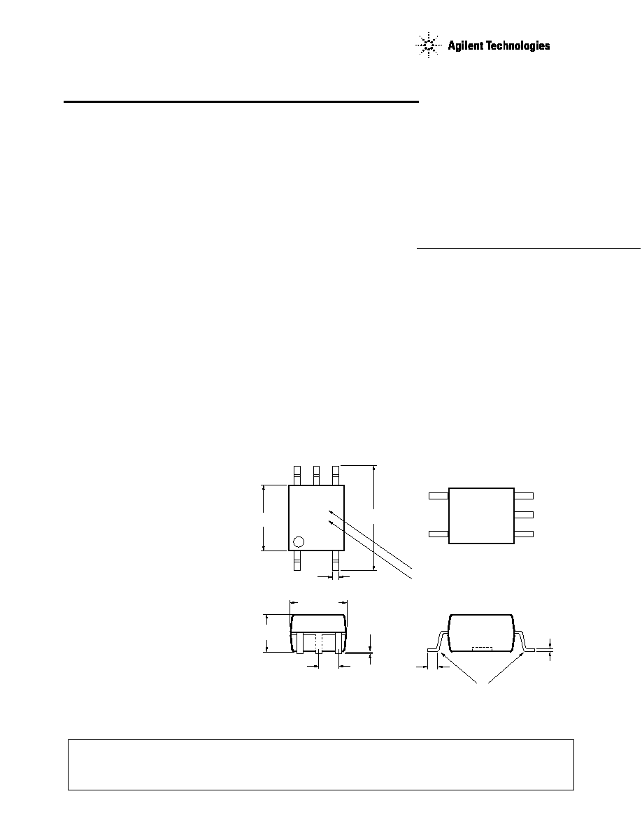
Outline Drawing (JEDEC MO-155)
CAUTION: The small junction sizes inherent to the design of this bipolar component increase the component's
susceptibility to damage from electrostatic discharge (ESD). It is advised that normal static precautions be taken
in handling and assembly of this component to prevent damage and/or degradation which may be induced by
ESD.
MXXX
XXX
6
5
4
3
1
7.0 ± 0.2
(0.276 ± 0.008)
2.5 ± 0.1
(0.098 ± 0.004)
0.102 ± 0.102
(0.004 ± 0.004)
VCC
VOUT
GND
CATHODE
ANODE
4.4 ± 0.1
(0.173 ± 0.004)
1.27
(0.050)
BSC
0.15 ± 0.025
(0.006 ± 0.001)
0.71
(0.028)
MIN.
0.4 ± 0.05
(0.016 ± 0.002)
3.6 ± 0.1*
(0.142 ± 0.004)
TYPE NUMBER (LAST 3 DIGITS)
DATE CODE
MAX. LEAD COPLANARITY
= 0.102 (0.004)
DIMENSIONS IN MILLIMETERS (INCHES)
* MAXIMUM MOLD FLASH ON EACH SIDE IS 0.15 mm (0.006)
NOTE: FLOATING LEAD PROTRUSION IS 0.15 mm (6 mils) MAX.
2
Description
The HCPL-M454 is similar to
Agilent's other high speed
transistor output optocouplers,
but with shorter propagation
delays and higher CTR. The
HCPL-M454 also has a
guaranteed propagation delay
difference (t
PLH
- t
PHL
). These
features make the HCPL-M454
an excellent solution to IPM
inverter dead time and other
switching problems.
The HCPL-M454 CTR, propaga-
tion delays, and CMR are
specified both for TTL load and
drive conditions and for IPM
(Intelligent Power Module) load
and drive conditions. Specifica-
tions and typical performance
plots for both TTL and IPM
conditions are provided for ease
of application.
This diode-transistor optocoupler
uses an insulating layer between
the light emitting diode and an
integrated photon detector to
provide electrical insulation
between input and output.
Separate connections for the
photodiode bias and output
transistor collector increase the
speed up to a hundred times over
that of a conventional photo-
transistor coupler by reducing the
base-collector capacitance.
Absolute Maximum Ratings
(No Derating Required up to 85
°
C)
Storage Temperature .................................................... -55
°
C to +125
°
C
Operating Temperature ................................................ -55
°
C to +100
°
C
Average Input Current - I
F
......................................................... 25 mA
[1]
Peak Input Current - I
F
.............................................................. 50 mA
[2]
(50% duty cycle, 1 ms pulse width)
Peak Transient Input Current - I
F
................................................... 1.0 A
(
1
µ
s pulse width, 300 pps)
Reverse Input Voltage - V
R
(Pin 3-1) .................................................. 5 V
Input Power Dissipation ........................................................... 45 mW
[3]
Average Output Current - I
O
(Pin 5) ............................................... 8 mA
Peak Output Current .................................................................... 16 mA
Output Voltage - V
O
(Pin 5-4) ............................................ -0.5 V to 20 V
Supply Voltage - V
CC
(Pin 6-4) .......................................... -0.5 V to 30 V
Output Power Dissipation ....................................................... 100 mW
[4]
Infrared and Vapor Phase Reflow Temperature ....................... see below
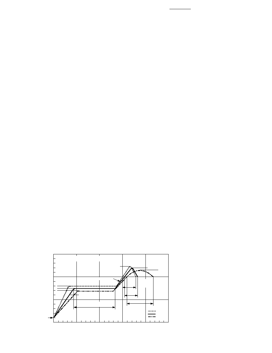
Solder Reflow Thermal Profile
0
TIME (SECONDS)
TEMPERATURE (°C)
200
100
50
150
100
200
250
300
0
30
SEC.
50 SEC.
30
SEC.
160°C
140°C
150°C
PEAK
TEMP.
245°C
PEAK
TEMP.
240°C
PEAK
TEMP.
230°C
SOLDERING
TIME
200°C
PREHEATING TIME
150°C, 90 + 30 SEC.
2.5°C ± 0.5°C/SEC.
3°C + 1°C/0.5°C
TIGHT
TYPICAL
LOOSE
ROOM
TEMPERATURE
PREHEATING RATE 3°C + 1°C/0.5°C/SEC.
REFLOW HEATING RATE 2.5°C ± 0.5°C/SEC.

3
Insulation Related Specifications
Parameter
Symbol
Value
Units
Conditions
Minimum External Air Gap
L(IO1)
5
mm
Measured from input terminals
(Clearance)
to output terminals
Minimum External Tracking Path
L(IO2)
5
mm
Measured from input terminals
(Creepage)
to output terminals
Minimum Internal Plastic Gap
0.08
mm
Through insulation distance
(Clearance)
conductor to conductor
Tracking Resistance
CTI
175
V
DIN IEC 112/VDE 0303 Part 1
Isolation Group (per DIN VDE 0109)
IIIa
Material Group DIN VDE 0109
Schematic
Land Pattern Recommendation
IF
SHIELD
6
5
4
GND
VCC
1
3
VO
ICC
VF
IO
ANODE
CATHODE
+
Recommended Pb-Free IR Profile
8.27
(0.325)
2.0
(0.080)
2.5
(0.10)
1.3
(0.05)
0.64
(0.025)
4.4
(0.17)
DIMENSION IN MILLIMETERS (INCHES)
217 °C
RAMP-DOWN
6 °C/SEC. MAX.
RAMP-UP
3 °C/SEC. MAX.
150 - 200 °C
260 +0/-5 °C
t 25 °C to PEAK
60 to 150 SEC.
20-40 SEC.
TIME WITHIN 5 °C of ACTUAL
PEAK TEMPERATURE
tp
ts
PREHEAT
60 to 180 SEC.
tL
TL
Tsmax
Tsmin
25
Tp
TIME
TEMPERA
TURE
NOTES:
THE TIME FROM 25 °C to PEAK TEMPERATURE = 8 MINUTES MAX.
Tsmax = 200 °C, Tsmin = 150 °C

4
DC Electrical Specifications
Over recommended temperature (T
A
= 0
°
C to 70
°
C) unless otherwise specified. (See note 11)
Parameter Symbol Min. Typ. Max. Units
Test Conditions
Fig. Note
Current
CTR
25
32
60
%
T
A
= 25
°
C V
O
= 0.4 V
I
F
= 16 mA 1,2,4
5
Transfer
Ratio
21
34
V
O
= 0.5 V
V
CC
= 4.5 V
Current
CTR
26
35
65
%
T
A
= 25
°
C V
O
= 0.4 V
I
F
= 12 mA 1,2,4
5
Transfer
Ratio
22
37
V
O
= 0.5 V
V
CC
= 4.5 V
Logic Low
V
OL
0.2
0.4
V
T
A
= 25
°
C I
O
= 3.0 mA
I
F
= 16 mA
Output
Voltage
0.2
0.5
I
O
= 2.4 mA
V
CC
= 4.5 V
Logic High
I
OH
0.003
0.5
µ
A
T
A
= 25
°
C V
O
= V
CC
= 5.5 V I
F
= 0 mA
5
Output
Current
0.01
1.0
T
A
= 25
°
C V
O
= V
CC
= 15 V
50
Logic Low
I
CCL
50
200
µ
A
I
F
= 16 mA V
CC
= 15 V
V
O
= open
11
Supply
Current
Logic High
I
CCH
0.02
1
µ
A
T
A
= 25
°
C I
F
= 0 mA
V
CC
= 15 V
11
Supply
V
O
= open
Current
0.02
2
Input
V
F
1.5
1.7
V
T
A
= 25
°
C I
F
= 16 mA
3
Forward
Voltage
1.5
1.8
Input
BV
R
5
V
I
R
= 10
µ
A
Reverse
Breakdown
Current
Tempera-
V
F
/
T
A
-1.6
mV/
°
C I
F
= 16 mA
ture Co-
efficient of
Forward
Voltage
Input
C
IN
60
pF
f = 1 MHz V
F
= 0 V
Capacitance
Input-
V
ISO
3750
V
RMS
RH < 50%
t = 1 min
6,12
Output
T
A
= 25
°
C
Insulation
Voltage
Resistance
R
I-O
10
[12]
V
I-O
= 500 Vdc
6
(Input-
Output)
Capacitance
C
I-O
0.6
pF
f = 1 MHz
6
(Input-
Output)

5
Switching Specifications
Over recommended temperature (T
A
= 0
°
C to 70
°
C) unless otherwise specified
Parameter
Sym.
Min. Typ. Max. Units
Test Conditions
Fig. Note
Propagation
t
PHL
0.2
0.3
µ
s
T
A
= 25
°
C Pulse: f = 20 kHz
8, 9
9
Delay Time
Duty Cycle = 10%
to Logic
0.2
0.5
I
F
= 16 mA
V
CC
= 5.0 V
Low at
R
L
= 1.9 k
C
L
= 15 pF
Output
V
THHL
= 1.5 V
0.2
0.5
0.7
T
A
= 25
°
C Pulse: f = 10 kHz
10-
10
Duty Cycle = 50%
14
0.1
0.5
1.0
I
F
= 12 mA
V
CC
= 15.0 V
R
L
= 20 k
C
L
= 100 pF
V
THHL
= 1.5 V
Propagation
t
PLH
0.3
0.5
µ
s
T
A
= 25
°
C Pulse: f = 20 kHz
8, 9
9
Delay Time
Duty Cycle = 10%
to Logic
0.3
0.7
I
F
= 16 mA
V
CC
= 5.0 V
High at
R
L
= 1.9 k
C
L
= 15 pF
Output
V
THLH
= 1.5 V
0.3
0.8
1.1
T
A
= 25
°
C Pulse: f = 10 kHz
10-
10
Duty Cycle = 50%
14
0.2
0.8
1.4
I
F
= 12 mA
V
CC
= 15.0 V
R
L
= 20 k
C
L
= 100 pF
V
THLH
= 2.0 V
Propagation
t
PLH
-
-0.4
0.3
0.9
µ
s
T
A
= 25
°
C Pulse: f = 10 kHz
10-
13
Delay
t
PHL
Duty Cycle = 50%
14
Difference
-0.7
0.3
1.3
I
F
= 12 mA
V
CC
= 15.0 V
Between
R
L
= 20 k
C
L
= 100 pF
Any 2 Parts
V
THHL
= 1.5 V
V
THLH
= 2.0 V
Common
|CM
H
|
15
30
kV/
µ
s T
A
= 25
°
C V
CC
= 5.0 V
R
L
= 1.9 k
7
7,9
Mode
C
L
= 15 pF
I
F
= 0 mA
Transient
V
CM
= 1500 V
P-P
Immunity
at Logic
15
30
T
A
= 25
°
C V
CC
= 15.0 V
R
L
= 20 k
7
8,10
High Level
C
L
= 100 pF
I
F
= 0 mA
Output
V
CM
= 1500 V
P-P
Common
|CM
L
|
15
30
kV/
µ
s T
A
= 25
°
C V
CC
= 5.0 V
R
L
= 1.9 k
7
7,9
Mode
C
L
= 15 pF
I
F
= 16 mA
Transient
V
CM
= 1500 V
P-P
Immunity
at Logic
10
30
T
A
= 25
°
C V
CC
= 15.0 V
R
L
= 20 k
7
8,10
Low Level
C
L
= 100 pF
I
F
= 12 mA
Output
V
CM
= 1500 V
P-P
15
30
T
A
= 25
°
C V
CC
= 15.0 V
R
L
= 20 k
7
8,10
C
L
= 100 pF
I
F
= 16 mA
V
CM
= 1500 V
P-P