HCPL-2530
Dual Channel, High Speed
Optocouplers
Technical Data
HCPL-2530
HCPL-0530
HCPL-2531
HCPL-0531
HCPL-4534
HCPL-0534
Features
· 15 kV/
µ
s Minimum Common
Mode Transient Immunity at
V
CM
= 1500 V
(HCPL-4534/0534)
· High Speed: 1 Mb/s
· TTL Compatible
· Available in 8 Pin DIP, SO-8,
and 8 Pin DIP Gull Wing
Surface Mount (Option 020)
Packages
· High Density Packaging
· 3 MHz Bandwidth
· Open Collector Outputs
· Guaranteed Performance
from 0
°
C to 70
°
C
· Safety Approval
UL Recognized 2500 V rms
for 1 minute (5000 V rms for
1 minute for Option 020) per
UL1577
CSA Approved
· Single Channel Version
Available (4502/3, 0452/3)
· MIL-STD-1772 Version
Available (55XX/65XX/4N55)
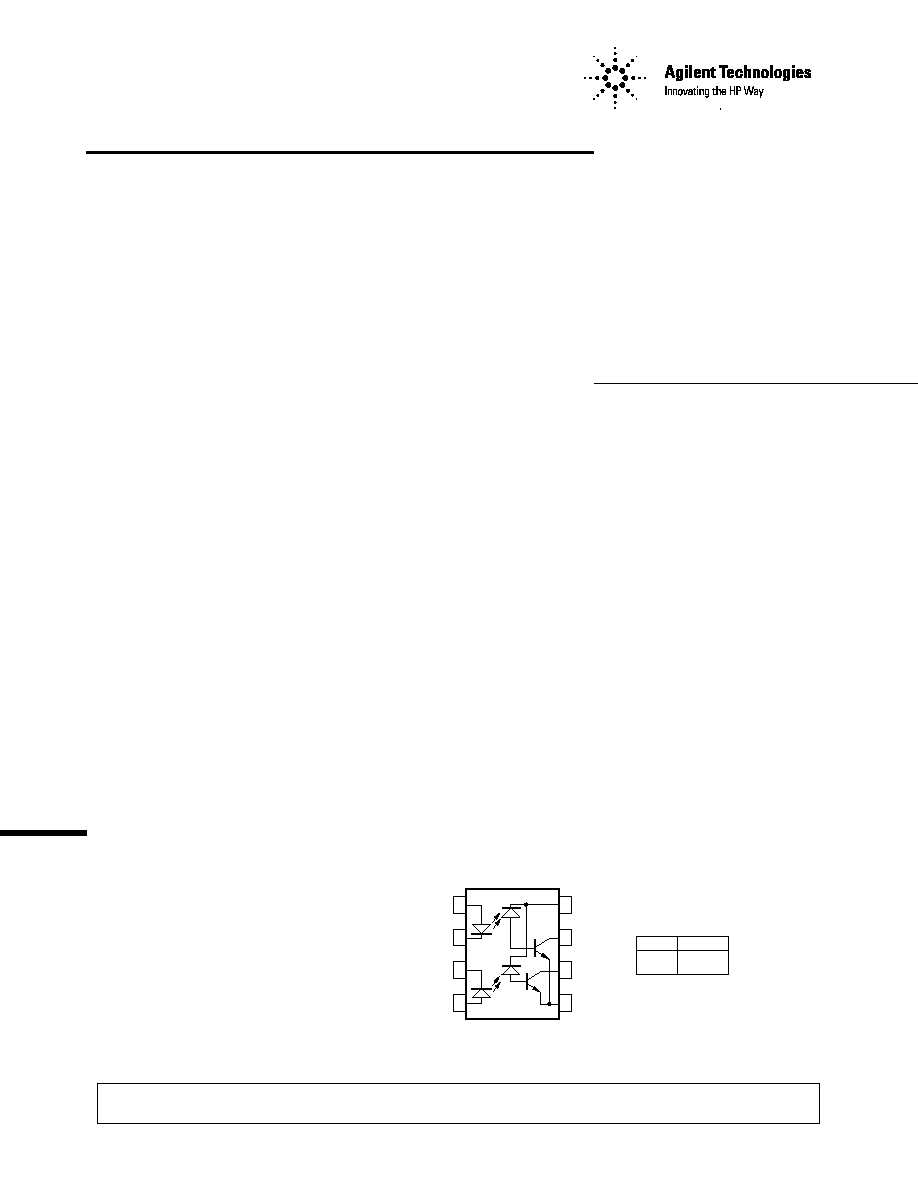
Functional Diagram
Applications
· Line Receivers High
Common Mode Transient
Immunity (>1000 V/
µ
s) and
Low Input-Output Capacitance
(0.6 pF)
· High Speed Logic Ground
Isolation TTL/TTL, TTL/
LTTL, TTL/CMOS, TTL/LSTTL
· Replace Pulse Transformers
Save Board Space and Weight
· Analog Signal Ground
Isolation Integrated Photon
Detector Provides Improved
Linearity over Phototransistor
Type
· Polarity Sensing
· Isolated Analog Amplifier
Dual Channel Packaging
Enhances Thermal Tracking
CAUTION: It is advised that normal static precautions be taken in handling and assembly of this component to
prevent damage and/or degradation which may be induced by ESD.
A 0.1
µ
F bypass capacitor between pins 5 and 8 is recommended.
7
1
2
3
4
5
6
8
ANODE 1
CATHODE 1
CATHODE 2
ANODE 2
VCC
VO1
VO2
GND
TRUTH TABLE
(POSITIVE LOGIC)
LED
ON
OFF
VO
LOW
HIGH
Description
These dual channel optocouplers
contain a pair of light emitting
diodes and integrated photodetec-
tors with electrical insulation
between input and output.
Separate connection for the
photodiode bias and output
transistor collectors increase the
speed up to a hundred times that
of a conventional phototransistor
coupler by reducing the base-
collector capacitance.
2
These dual channel optocouplers
are available in an 8 Pin DIP and
in an industry standard SO-8
package. The following is a cross
reference table listing the 8 Pin
DIP part number and the
electrically equivalent SO-8 part
number.
SO-8
8 Pin DIP
Package
HCPL-2530
HCPL-0530
HCPL-2531
HCPL-0531
HCPL-4534
HCPL-0534
The SO-8 does not require
"through holes" in a PCB. This
package occupies approximately
one-third the footprint area of the
standard dual-in-line package.
The lead profile is designed to be
compatible with standard surface
mount processes.
The HCPL-2530/0530 is for use in
TTL/CMOS, TTL/LSTTL or wide
bandwidth analog applications.
Current transfer ratio (CTR) for
the HCPL-2530/0530 is 7%
minimum at I
F
= 16 mA.
The HCPL-2531/0531 is designed
for high speed TTL/TTL
applications. A standard 16 mA
TTL sink current through the
input LED will provide enough
output current for 1 TTL load and
a 5.6 k
pull-up resistor. CTR of
the HCPL-2531/0531 is 19%
minimum at I
F
= 16 mA.
The HCPL-4534/0534 is an
HCPL-2531/0531 with increased
common mode transient immunity
of 15,000 V/
µ
s minimum at
V
CM
= 1500 V guaranteed.
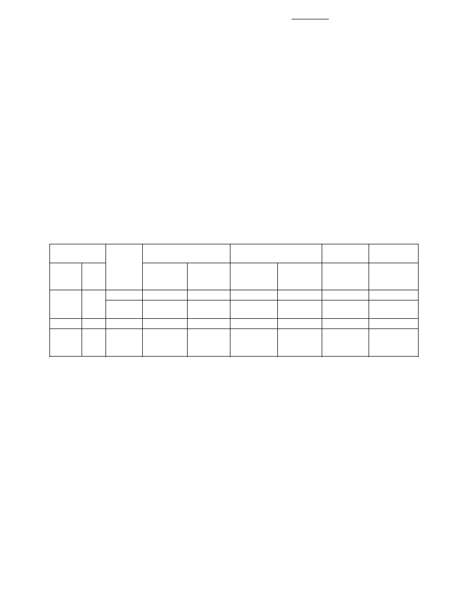
Selection Guide
Widebody
Minimum CMR
8-pin DIP (300 Mil)
Small-Outline SO-8
(400 Mil)
Hermetic
Current
Dual
Single
Dual
Single
Single
Single and
dV/dt
V
CM
Transfer
Channel
Channel
Channel
Channel
Channel
Dual Channel
(V/
µ
s)
(V)
Ratio (%)
Package
Package*
Package
Package*
Package*
Packages*
1,000
10
7
HCPL-2530
6N135
HCPL-0530
HCPL-0500
HCNW135
19
HCPL-2531
6N136
HCPL-0531
HCPL-0501
HCNW136
HCPL-4502
HCPL-0452
HCNW4502
15,000
1500
19
HCPL-4534
HCPL-4503
HCPL-0534
HCPL-0453
HCNW4503
1,000
10
9
HCPL-55XX
HCPL-65XX
4N55
*Technical data for these products are on separate Agilent publications.
3
Ordering Information
Specify Part Number followed by Option Number (if desired).
Example:
HCPL-2531#XXX
020 = UL 5000 V rms/1 Minute Option*
300 = Gull Wing Surface Mount Option
500 = Tape and Reel Packaging Option
Option data sheets available. Contact your Agilent sales representative or authorized distributor for
information.
*For HCPL-2530/1 and HCPL-4534 only.
Gull wing surface mount option applies to through hole parts only.
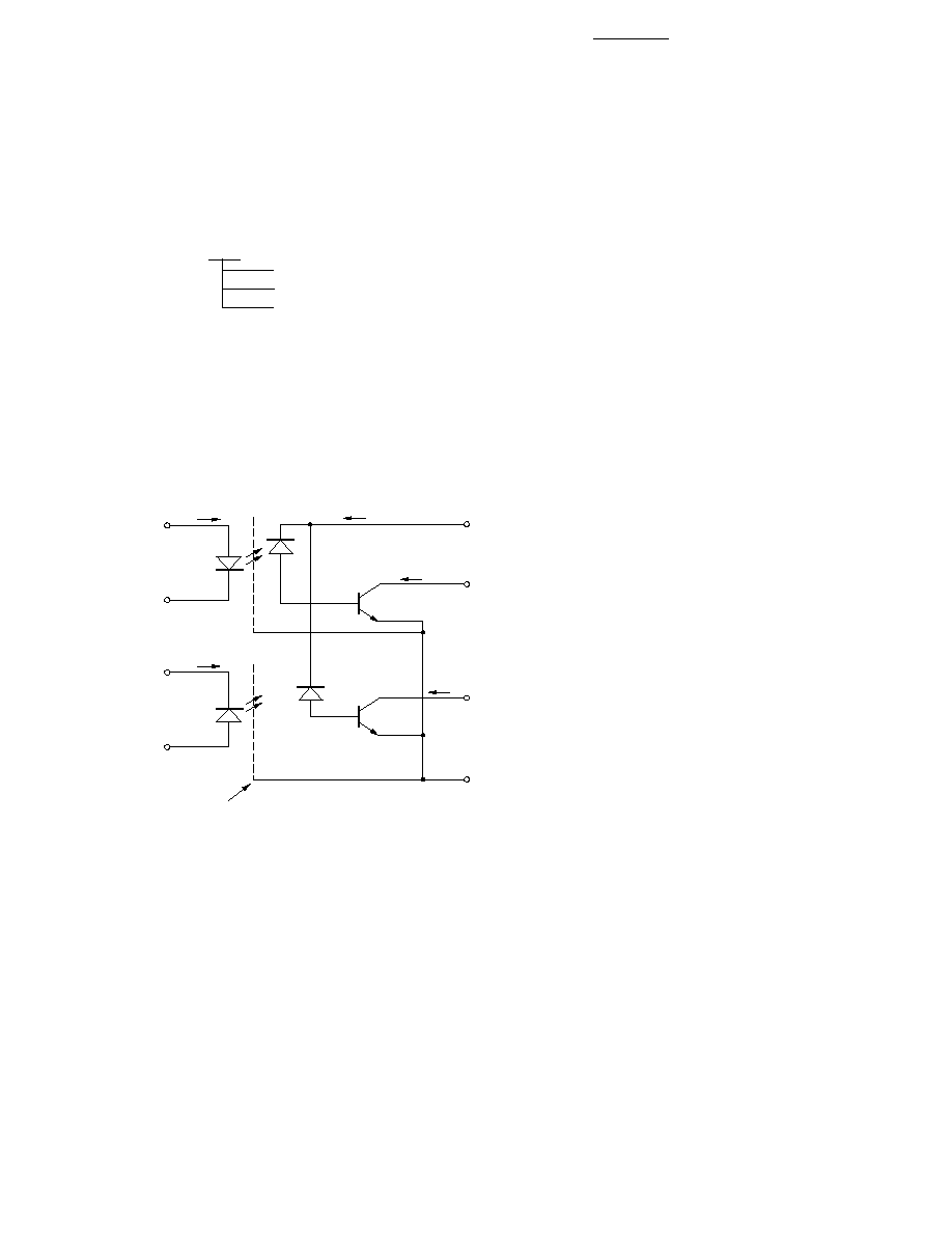
Schematic
IF1
HCPL-4534/0534 SHIELD
8
7
VCC
+
2
VO1
ICC
VF1
I O1
1
IF2
6
5
GND
4
VO2
VF2
I O2
3
+
USE OF A 0.1 µF BYPASS CAPACITOR CONNECTED
BETWEEN PINS 5 AND 8 IS RECOMMENDED.
4
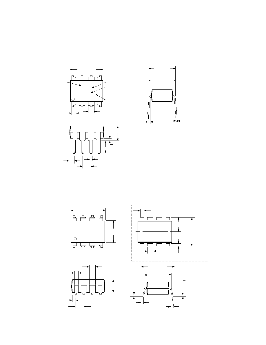
Package Outline Drawings
8-Pin DIP Package (HCPL-2530/2531/4534)
8-Pin DIP Package with Gull Wing Surface Mount Option 300 (HCPL-2530/2531/4534)
0.635 ± 0.25
(0.025 ± 0.010)
12° NOM.
9.65 ± 0.25
(0.380 ± 0.010)
0.635 ± 0.130
(0.025 ± 0.005)
7.62 ± 0.25
(0.300 ± 0.010)
5
6
7
8
4
3
2
1
9.65 ± 0.25
(0.380 ± 0.010)
6.350 ± 0.25
(0.250 ± 0.010)
1.016 (0.040)
1.194 (0.047)
1.194 (0.047)
1.778 (0.070)
9.398 (0.370)
9.906 (0.390)
4.826
(0.190)
TYP.
0.381 (0.015)
0.635 (0.025)
PAD LOCATION (FOR REFERENCE ONLY)
1.080 ± 0.320
(0.043 ± 0.013)
4.19
(0.165)
MAX.
1.780
(0.070)
MAX.
1.19
(0.047)
MAX.
2.54
(0.100)
BSC
DIMENSIONS IN MILLIMETERS (INCHES).
LEAD COPLANARITY = 0.10 mm (0.004 INCHES).
0.254
+ 0.076
- 0.051
(0.010
+ 0.003)
- 0.002)
9.65 ± 0.25
(0.380 ± 0.010)
1.78 (0.070) MAX.
1.19 (0.047) MAX.
A XXXXZ
YYWW
DATE CODE
1.080 ± 0.320
(0.043 ± 0.013)
2.54 ± 0.25
(0.100 ± 0.010)
0.51 (0.020) MIN.
0.65 (0.025) MAX.
4.70 (0.185) MAX.
2.92 (0.115) MIN.
DIMENSIONS IN MILLIMETERS AND (INCHES).
5
6
7
8
4
3
2
1
5° TYP.
OPTION CODE*
UL
RECOGNITION
UR
0.254
+ 0.076
- 0.051
(0.010
+ 0.003)
- 0.002)
7.62 ± 0.25
(0.300 ± 0.010)
6.35 ± 0.25
(0.250 ± 0.010)
TYPE NUMBER
* MARKING CODE LETTER FOR OPTION NUMBERS.
"L" = OPTION 020
OPTION NUMBERS 300 AND 500 NOT MARKED.
5
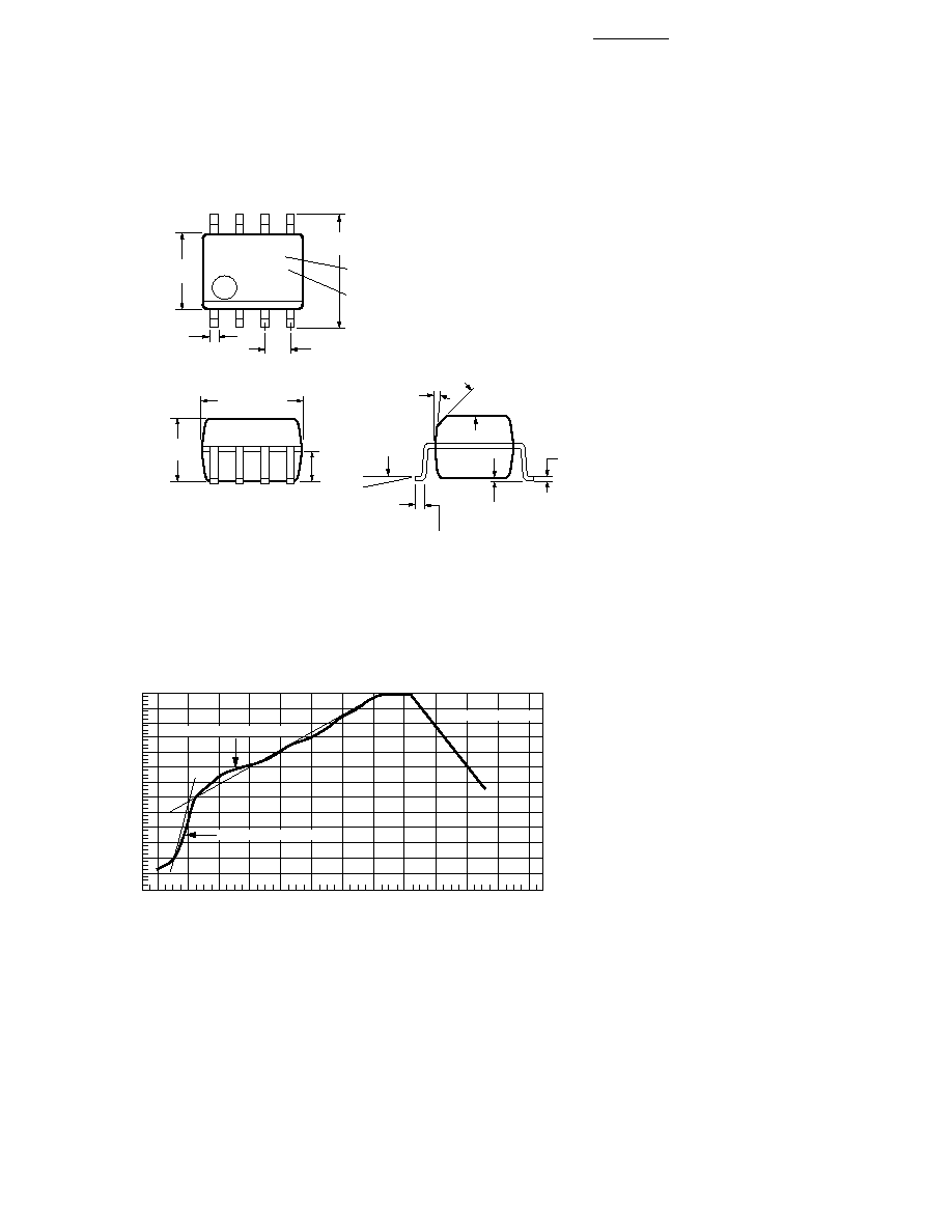
Small Outline SO-8 Package (HCPL-0530/0531/0534)
Note: Use of nonchlorine activiated fluxes is highly recommended.
240
T = 115°C, 0.3°C/SEC
0
T = 100°C, 1.5°C/SEC
T = 145°C, 1°C/SEC
TIME MINUTES
TEMPERATURE °C
220
200
180
160
140
120
100
80
60
40
20
0
260
1
2
3
4
5
6
7
8
9
10
11
12
Solder Reflow Temperature Profile (HCPL-0530/0531/0534 and Gull Wing Surface
Mount Option Parts)
Regulatory Information
The devices contained in this data
sheet have been approved by the
following organizations:
UL
Recognized under UL 1577,
Component Recognition
Program, File E55361.
CSA
Approved under CSA Component
Acceptance Notice #5, File CA
88324.
XXX
YWW
8
7
6
5
4
3
2
1
5.994 ± 0.203
(0.236 ± 0.008)
3.937 ± 0.127
(0.155 ± 0.005)
0.406 ± 0.076
(0.016 ± 0.003)
1.270
(0.050)
BSG
5.080 ± 0.127
(0.200 ± 0.005)
3.175 ± 0.127
(0.125 ± 0.005)
1.524
(0.060)
45° X
0.432
(0.017)
0.228 ± 0.025
(0.009 ± 0.001)
TYPE NUMBER
(LAST 3 DIGITS)
DATE CODE
0.305
(0.012)
MIN.
TOTAL PACKAGE LENGTH (INCLUSIVE OF MOLD FLASH)
5.207 ± 0.254 (0.205 ± 0.010)
DIMENSIONS IN MILLIMETERS (INCHES).
LEAD COPLANARITY = 0.10 mm (0.004 INCHES) MAX.
0.203 ± 0.102
(0.008 ± 0.004)
7°
PIN ONE
0 ~ 7°
*
*
Document Outline