Document Outline
- List of Figures
- 1. Output Power and Collector Efficiency vs. Input Power
- 2. Output Power vs. Input Power Over Bias Voltage
- 3. Collector Efficiency vs. Input Power Over Bias Voltage
- 4. Output Power vs. Input
- 5. IMD 3 , IMD 5 vs. Output Power Per Tone
- 6. Input and Output Return Loss vs. Frequency
- 7. Output Power and Collector Efficiency vs. Input Power
- 8. Output Power vs. Input Power Over Bias Voltage
- 9. Collector Efficiency vs. InputPower Over Bias Voltage
- 10. Input and Output Return Loss vs. Frequency
- 11. Collector-Base Capacitance vs. Collector-Base Voltage (DC Test)
- 12. Insertion Power Gain, Maximum Available Gain, and Maximum Stable Gain vs. Frequency, VCE = 3.6 V, IC = 200 mA
- 13. Insertion Power Gain, Maximum Available Gain, and Maximum Stable Gain vs. Frequency, VCE = 4.8 V, IC = 150 mA
- 14. Insertion Power Gain, Maximum Available Gain, and Maximum Stable Gain vs. Frequency, VCE = 6.0 V, IC = 150 mA
- Features
- Applications
- MSOP-3 Surface Mount Plastic Package
- Pin Configuration
- Description
- AT-33225 Absolute Maximum Ratings
- Electrical Specifications, TC = 25°C
- AT-33225 Typical Performance, TC = 25°C
- AT-33225 Typical Performance, TC = 25°C
- AT-33225 Typical Large Signal Impedances
- SPICE Model Parameters
- AT-33225 Typical Scattering Parameters, Common Emitter, Z O = 50 W
- Typical Performance
- Test Circuit A: Test Circuit Board Layout @ 900 MHz (ETACS/ISM)
- Test Circuit A: Test Circuit Schematic Diagram @ 900 MHz (ETACS/ISM)
- Test Circuit B: Test Circuit Board Layout @ 836.5 MHz (AMPS)
- Test Circuit B: Test Circuit Schematic Diagram @ 836.5 MHz (AMPS)
- Part Number Ordering Information
- Package Dimensions
- Tape Dimensions and Product Orientation for Package MSOP-3

4-71
4.8 V NPN Common Emitter
Output Power Transistor
for AMPS, ET ACS Phones
Technical Data
Features
· 4.8 Volt Operation
· +31.0 dBm P
out
@ 900 MHz,
Typ.
· 70% Collector Efficiency
@ 900 MHz, Typ.
· 9 dB Power Gain @ 900 MHz,
Typ.
· -29 dBc IMD
3
@ P
out
of
24 dBm per tone, 900 MHz,
Typ.
· Internal Input Pre-Matching
Facilitates Cascading
· 50% Smaller than SOT-223
Package
Applications
· Output Power Device for
AMPS and ETACS Handsets
· 900 MHz ISM
AT-33225
Description
Hewlett Packard's AT-33225 is a
low cost, NPN power silicon
bipolar junction transistor housed
in a miniature MSOP-3 surface
mount plastic package. This
device is designed for use as an
output device for AMPS and
ETACS mobile phones. The
AT-33225 features over 1 watt
CW output power when operated
at 4.8 volts. Excellent gain and
superior efficiency make the
AT-33225 ideal for use in battery
powered systems.
The AT-33225 is fabricated with
Hewlett Packard's 10 GHz F
t
Self-
Aligned-Transistor (SAT) process.
The die are nitride passivated for
surface protection. Excellent
device uniformity, performance
and reliability are produced by the
use of ion-implantation, self-
alignment techniques, and gold
metalization in the fabrication of
these devices.
MSOP-3 Surface Mount
Plastic Package
Outline 25
Pin Configuration
EMITTER
1
2
BASE
3
EMITTER
COLLECTOR
4
5965-5910E

4-72
AT-33225 Absolute Maximum Ratings
Absolute
Symbol
Parameter
Units
Maximum
[1]
V
EBO
Emitter-Base Voltage
V
1.4
V
CBO
Collector-Base Voltage
V
16.0
V
CEO
Collector-Emitter Voltage
V
9.5
I
C
Collector Current
mA
640
P
T
Power Dissipation
[2]
W
1.6
T
j
Junction Temperature
°
C
150
T
STG
Storage Temperature
°
C
-65 to 150
Thermal Resistance
[3]
:
jc
= 40
°
C/W
Notes:
1. Permanent damage may occur if
any of these limits are exceeded.
2. Derate at 25 mW/
°
C for T
C
> 85
°
C.
T
c
is defined to be the temperature
of the collector pin 4, where the
lead contacts the circuit board.
3. Using the liquid crystal technique,
V
CE
= 4.5 V, I
c
= 100 mA, T
j
=150
°
C,
1- 2
µ
m "hot-spot" resolution.
Electrical Specifications, T
C
= 25
°
C
Symbol
Parameters and Test Conditions
Units Min.
Typ. Max.
Freq. = 900 MHz, V
CE
= 4.8 V, I
CQ
= 6 mA, CW operation, Test Circuit A,
unless otherwise specified
P
out
Output Power
[1]
P
in
= +22 dBm
dBm
+30.0
+31.0
C
Collector Efficiency
[1]
P
in
= +22 dBm
%
60
70
IMD
3
3rd Order Intermodulation Distortion, 2 Tone Test,
F1 = 899 MHz
dBc
-29
P
out
each Tone = +24 dBm
[1]
F2 = 901 MHz
Mismatch Tolerance, No Damage
[1]
P
out
= +31 dBm
7:1
any phase, 2 sec duration
BV
EBO
Emitter-Base Breakdown Voltage
I
E
= 0.4 mA, open collector
V
1.4
BV
CBO
Collector-Base Breakdown Voltage
I
C
= 2.0 mA, open emitter
V
16.0
BV
CEO
Collector-Emitter Breakdown Voltage
I
C
= 10.0 mA, open base
V
9.5
h
FE
Forward Current Transfer Ratio
V
CE
= 3 V, I
C
= 180 mA
--
80
150
330
I
CEO
Collector Leakage Current
V
CEO
= 5 V
µ
A
30
Note:
1. With external matching on input and output, tested in a 50 ohm environment. Refer to Test Circuit A (ETACS/ISM).

4-73
AT-33225 Typical Performance, T
C
= 25
°
C
Frequency = 900 MHz, V
CE
= 4.8 V, I
CQ
= 6 mA, CW operation, Test Circuit A (ETACS/ISM), unless otherwise specified.
6
9
12
33
15
18
21
24
27
30
0
10
20
30
40
90
80
50
60
70
2
14
6
10
18
24
22
OUTPUT POWER
(dBm)
COLLECTOR EFFICIENCY
(%)
INPUT POWER (dBm)
Figure 1. Output Power and Collector
Efficiency vs. Input Power.
0
10
15
5
20
35
30
25
OUTPUT POWER
(dBm)
INPUT POWER (dBm)
Figure 2. Output Power vs. Input
Power Over Bias Voltage.
0
20
10
30
40
90
80
70
50
60
COLLECTOR EFFICIENCY
(%)
INPUT POWER (dBm)
Figure 3. Collector Efficiency vs.
Input Power Over Bias Voltage.
Figure 5. IMD
3
, IMD
5
vs. Output
Power Per Tone.
Figure 6. Input and Output Return
Loss vs. Frequency.
2
14
6
10
18
24
22
2
14
6
10
18
24
22
2
14
6
10
18
24
22
Pout
c
source = 0.82
-163
load = 0.67
-174
source = 0.82
-163
load = 0.67
-174
6
14
10
18
22
34
26
30
OUTPUT POWER
(dBm)
INPUT POWER (dBm)
Figure 4. Output Power vs. Input
Power Over Temperature.
T
C
= +85
°
C
T
C
= +25
°
C
T
C
= 40
°
C
3.6 V
4.8 V
6.0 V
source = 0.82
-163
load = 0.67
-174
3.6 V
4.8 V
6.0 V
source = 0.82
-163
load = 0.67
-174
source = 0.82
-163
load = 0.67
-174
-45
-40
-35
-30
-15
-25
-20
IMD
(dBc)
OUTPUT POWER/TONE (dBm)
11
17
13
15
19
21
25
27
23
IMD3
IMD5
source = 0.82
-163
load = 0.67
-174
-30
-25
-20
-15
5
-10
-5
0
RETURN LOSS
(dB)
FREQUENCY (MHz)
800
850
950
1000
900
Output R.L.
Input R.L.

4-74
AT-33225 Typical Performance, T
C
= 25
°
C
Frequency = 836.5 MHz, V
CE
= 4.8 V, I
CQ
= 6 mA, CW operation, Test Circuit B (AMPS), unless otherwise specified.
6
9
12
33
15
18
21
24
27
30
0
10
20
30
40
90
80
50
60
70
OUTPUT POWER
(dBm)
COLLECTOR EFFICIENCY
(%)
INPUT POWER (dBm)
Figure 7. Output Power and Collector
Efficiency vs. Input Power.
OUTPUT POWER
(dBm)
INPUT POWER (dBm)
Figure 8. Output Power vs. Input
Power Over Bias Voltage.
COLLECTOR EFFICIENCY
(%)
INPUT POWER (dBm)
Figure 9. Collector Efficiency vs.
InputPower Over Bias Voltage.
Pout
c
source = 0.81
-165
load = 0.66
-174
Figure 10. Input and Output Return
Loss vs. Frequency.
2
14
6
10
18
24
22
0
10
15
5
20
35
30
25
2
14
6
10
18
24
22
source = 0.81
-165
load = 0.66
-174
3.6 V
4.8 V
6.0 V
0
20
10
30
40
90
80
70
50
60
2
14
6
10
18
24
22
source = 0.81
-165
load = 0.66
-174
3.6 V
4.8 V
6.0 V
source = 0.81
-165
load = 0.66
-174
-25
-20
-15
-10
5
-5
0
RETURN LOSS
(dB)
FREQUENCY (MHz)
750
800
850
950
900
836.5
Output R.L.
Input R.L.
4-75
SPICE Model Parameters
Die Model
Packaged Model
AT-33225 Typical Large Signal Impedances
V
CE
= 4.8 V, I
CQ
= 6 mA, P
out
= +31.0 dBm
Freq.
source
load
MHz
Mag.
Ang.
Mag.
Ang.
750
0.77
-162
0.64
-174
800
0.80
-169
0.67
-173
850
0.82
-164
0.64
-175
900
0.82
-163
0.67
-174
950
0.83
-166
0.74
-175
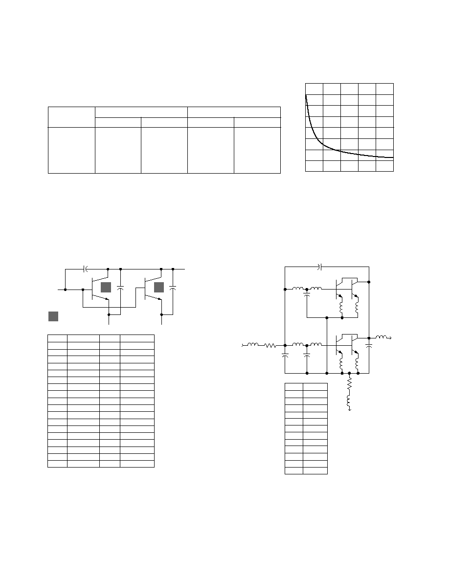
6.0
6.5
7.0
10.0
9.5
8.5
9.0
7.5
8.0
0
4
6
2
10
8
Ccb
(pF)
Vcb (V)
Figure 11. Collector-Base
Capacitance vs. Collector-Base
Voltage (DC Test).
C
CPad
CPad
Die Area = 1.2
CPad = 0.3 pF
E1
B
E2
CPad
Label
BF
IKF
ISE
NE
VAF
NF
TF
XTF
VTF
ITF
PTF
XTB
BR
IKR
ISC
NC
VAR
NR
Value
280
299.9
9.9E-11
2.399
33.16
0.9935
1.6E-11
0.006656
0.02785
0.001
23
0
54.61
81
8.7E-13
1.587
1.511
0.9886
Label
TR
EG
IS
XTI
CJC
VJC
MJC
XCJC
FC
CJE
VJE
MJE
RB
IRB
RBM
RE
RC
Value
1E-9
1.11
3.598E-15
3
0.8E-12
0.4831
0.2508
0.001
0.999
6.16E-12
1.186
0.5965
0.752
0
0.01
1.27
0.107
B
C
LE2
CM
RB
LB2
RB
LB3
Cbc
LE2
Die
LE2
CM
RB
LB2
LB1
R1
RB
LB3
Cbe
Cce
LE2
Die
LC1
R1
LE1
E
Label
Cbc
Cbe
Cce
CM
LB1
LB2
LB3
LE1
LE2
LC1
RB
R1
Value
0.80 pF
0.006 pF
3.17 pF
20.8 pF
0.63 nH
0.10 nH
0.87 nH
0.35 nH
0.78 nH
0.74 nH
0.1
0.2