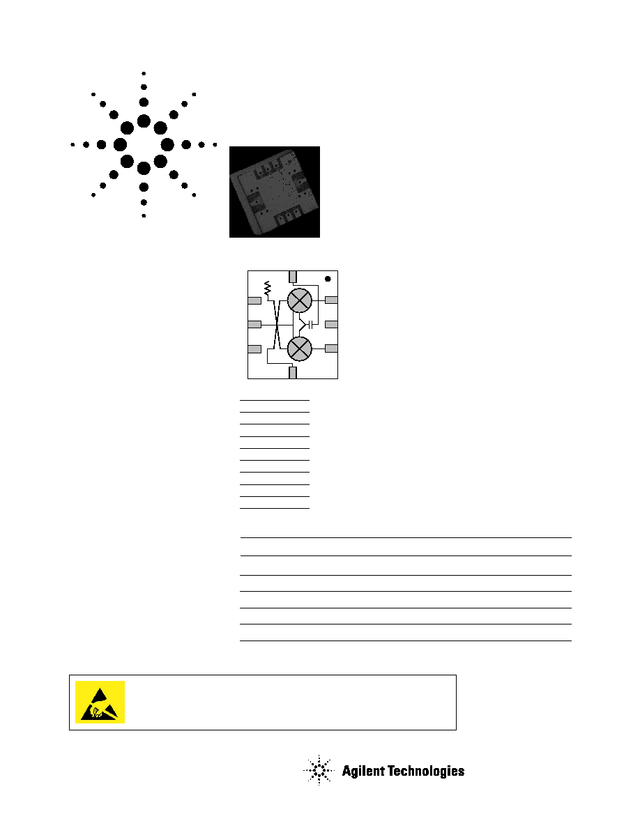
Agilent AMMP-6530
5 30 GHz Image Reject Mixer
Data Sheet
Description
Agilent's AMMP-6530 is an image
reject mixer that operates from
5 GHz to 30 GHz. The cold
channel FET mixer is designed to
be an easy-to-use component for
any surface mount PCB applica-
tion. It can be used drain pumped
for low conversion loss applica-
tions, or when gate pumped the
mixer can provide high linearity
for SSB up-conversion. An
external 90-degree hybrid is used
to achieve image rejection and a
-1V voltage reference is needed.
Intended applications include
microwave radios, 802.16, VSAT,
and satellite receivers. Since this
one mixer can cover several
bands, the AMMP-6530 can
reduce part inventory. The
integrated mixer eliminates
complex tuning and assembly
processes typically required by
hybrid (discrete-FET or diode)
mixers. The package is fully SMT
compatible with backside ground-
ing and I/O to simplify assembly.
Absolute Maximum Ratings
[1]
Symbol
Parameters/Conditions
Units
Min.
Max.
V
g
Gate Supply Voltage
V
0
-3
P
in
CW Input Power
dBm
15
T
ch
Operating Channel Temperature
°C
+150
T
stg
Storage Case Temperature
°C
-65
+150
T
max
Max. Assembly Temp (60 sec max)
°C
+300
Note:
1. Operation in excess of any one of these conditions may result in permanent damage to this device.
Features
· 5x5 mm Surface Mount Package
· Broad Band Performance 5 30 GHz
· Low Conversion Loss of 8 dB
· High Image Rejection of 15 20 dB
· Good 3rd Order Intercept of
+18 dBm
· Single -1V, no current Supply Bias
Applications
· Microwave Radio Systems
· Satellite VSAT, DBS Up/Down Link
· LMDS & Pt-Pt mmW Long Haul
· Broadband Wireless Access
(including 802.16 and 802.20
WiMax)
· WLL and MMDS loops
· Commercial grade military
8
4
7
1
2
3
6
5
RF
NC
IF1
NC
IF2
Vg
NC
gate
Attention: Observe precautions for handling electrostatic sensitive devices.
ESD Machine Model (Class A)
ESD Human Body Model (Class 0)
Refer to Agilent Application Note A004R: Electrostatic Discharge Damage and Control.
Top view
package base: GND
Pin
Function
1
IF1
2
3
IF2
4
LO
5
6
Vg
7
8
RF

2
AMMP-6530 Typical Performance
[2, 3]
(T
A
= 25
°C, V
g
= -1V, IF frequency = 1 GHz, Z
o
=50
)
Symbol
Parameters and Test Conditions
Units
Gate Pumped
Drain Pumped
F
RF
RF Frequency Range
GHz
5 30
5 30
F
LO
LO Frequency Range
GHz
5 30
5 30
F
IF
IF Frequency Range
GHz
DC 5
DC 5
Down Conversion
Up Conversion
Down Conversion
P
LO
LO Port Pumping Power
dBm
>10
>0
>10
CG
RF to IF Conversion Gain
dB
-10
-15
-8
RL_RF
RF Port Return Loss
dB
5
5
10
RL_LO
LO Port Return Loss
dB
10
10
5
RL_IF
IF Port Return Loss
dB
10
10
10
IR
Image Rejection Ratio
dB
15
15
15
LO-RF Iso.
LO to RF Port Isolation
dB
22
25
22
LO-IF Iso.
LO to IF Port Isolation
dB
25
25
25
RF-IF Iso.
RF to IF Port Isolation
dB
15
15
15
IIP3
Input IP3, Fdelta=100 MHz,
dBm
18
--
10
Prf = -10 dBm, Plo = 15 dBm
P-1
Input Port Power at 1dB gain
dBm
8
--
0
compression point, Plo=+10 dBm
NF
Noise Figure
dB
10
--
12
Notes:
2. Small/Large signal data measured in a fully de-embedded test fixture form T
A
= 25
°C.
3. Specifications are derived from measurements in a 50
test environment.
AMMP-6530 RF Specifications in Drain Pumped Test Configuration
[4, 5, 6, 7]
(T
A
= 25
°C, V
g
= -1.0V, P
LO
= +10 dBm, Z
o
= 50
)
Symbol
Parameters and Test Conditions
Units
Typ.
Sigma
CG
Conversion Gain
dB
-8
0.5
IR
Image Rejection Ratio
dB
20
1.0
Notes:
4. Pre-assembly into package performance verified 100% on-wafer.
5. 100% on-wafer RF testing is done at RF frequency = 7, 18, and 28 GHz; IF frequency = 2 GHz.
6. This final package part performance is verified by a functional test correlated to actual performance.
7. The external 90 degree hybrid coupler is from M/A-COM: PN 2032-6344-00. Frequency 1.0 2.0 GHz.
AMMP-6530 DC Specifications/Physical Properties
[1]
Symbol
Parameters and Test Conditions
Units
Typ.
I
g
Gate Supply Current (under any RF power drive and temperature)
mA
0
V
g
Gate Supply Operating Voltage
V
-1V
Note:
1. Ambient operational temperature T
A
=25
°C unless otherwise noted.

3
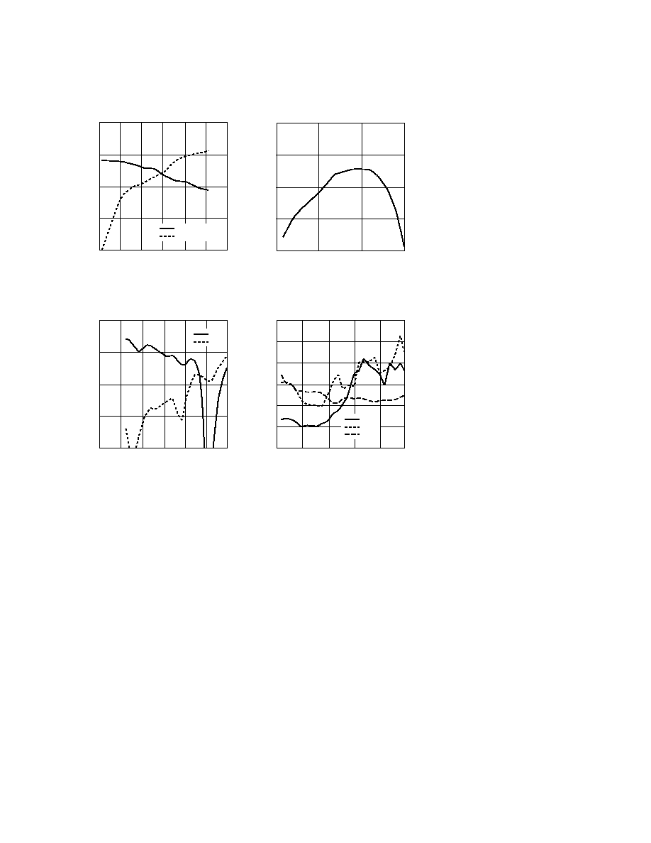
AMMP-6530 Typical Performance under Gate Pumped Down Conversion Operation
(T
A
= 25
°C, V
g
= -1V, Z
o
= 50
)
Figure 1. Conversion Gain with IF
terminated for Low Side Conversion
LO=+10 dBm, IF=1 GHz.
FREQUENCY (GHz)
CONVERSION GAIN (dB)
0
-5
-10
-15
-20
-25
-30
-35
-40
-45
-50
5
30
15
10
20
25
USB(dB)
LSB(dB)
Figure 2. Conversion Gain with IF
terminated for High Side Conversion
LO=+10 dBm, IF=1 GHz.
FREQUENCY (GHz)
CONVERSION GAIN (dB)
0
-5
-10
-15
-20
-25
-30
-35
-40
-45
-50
5
30
15
10
20
25
USB(dB)
LSB(dB)
Figure 3. RF Port Input Power P-1dB.
LO=+10 dBm, IF=1 GHz.
FREQUENCY (GHz)
INPUT POWER (dB)
15
10
5
0
-5
5
30
15
10
20
25
Figure 4. Noise Figure.
LO=+7 dBm, IF=1 GHz.
FREQUENCY (GHz)
NOISE FIGURE (dB)
20
15
10
5
0
5
30
15
10
20
25
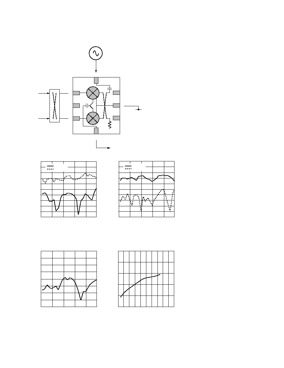
Figure 5. Input 3rd Order Intercept Point.
IF=1 GHz.
FREQUENCY (GHz)
IIP3 (dBm)
25
20
15
10
5
5
30
15
10
20
25
Plo=10(dBm)
Plo=15(dBm)
Figure 6. Conversion Gain vs. LO Power.
RF=21 GHz (-20 dBm), LO=20 GHz.
LO POWER (dBm)
CONVERSION GAIN (dB)
0
-5
-10
-15
-20
-25
-10
20
0
-5
5
10
15
8
4
7
1
2
3
6
5
drain
RF
LO
LSB
USB
Note: The external 90
° hybrid coupler
is from M/A-COM: PN 2032-6344-00.
Frequency is 1.0 2.0 GHz.
-1V
NC
IF1
NC
IF2
Vg
NC
gate
4
AMMP-6530 Typical Performance under Gate Pumped Down Conversion
Operation (T
A
= 25
°C, V
g
= -1V, Z
o
=50
)
Figure 7. Conversion Gain and Match vs.
IF Frequency. RF=20 GHz, LO=10 dBm.
FREQUENCY (GHz)
CONVERSION GAIN (dB),
RETURN LOSS (dB)
0
-5
-10
-15
-20
0
6
2
1
3
5
4
Conv. Gain (dB)
Return Loss (dB)
Figure 8. Conversion Gain vs. Gate Voltage.
RF=20 GHz, LO=10 dBm.
Vg (V)
CONVERSION GAIN (dB)
0
-5
-10
-15
-20
-2
-0.5
-1.5
-1
Figure 9. RF & LO Return Loss. LO=10 dBm.
FREQUENCY (GHz)
RETURN LOSS (dB)
0
-5
-10
-15
-20
0
30
15
10
5
20
25
RF
LO
Figure 10. Isolation. LO=+10 dBm, IF=1 GHz.
FREQUENCY (GHz)
ISOLATION (dB)
60
50
40
30
20
10
0
5
30
15
10
20
25
RF-IF
LO-IF
LO-RF
5
Figure 11. Up-conversion Gain with IF
terminated for Low Side Conversion.
LO=+5 dBm, IF=+5 dBm, IF=1 GHz.
FREQUENCY (GHz)
CONVERSION GAIN (dB)
0
-5
-10
-15
-20
-25
-30
-35
-40
-45
-50
5
30
15
10
20
25
USB (dB)
LSB (dB)
Figure 12. Up-conversion Gain wth IF
terminated for High Side Conversion.
LO=+5 dBm, IF=+5 dBm, IF=1 GHz.
FREQUENCY (GHz)
CONVERSION GAIN (dB)
0
-5
-10
-15
-20
-25
-30
-35
-40
-45
-50
5
30
15
10
20
25
USB (dB)
LSB (dB)
Figure 13. LO-RF Up-conversion Isolation.
FREQUENCY (GHz)
ISOLATION (dB)
0
-5
-10
-15
-20
-25
-30
-35
-40
5
30
15
10
20
25
Figure 14. Up-conversion Gain vs. Pumping
Power. LO power=IF power, IF=1 GHz,
RF=25 GHz.
PLO=PIF (dB)
CONVERSION LOSS (dB)
-5
-7
-9
-11
-13
-15
0
20
6
4
8
12
16
18
2
10
14
AMMP-6530 Typical Performance under Gate Pumped Up Conversion
Operation (T
A
= 25
°C, V
g
= -1V, Z
o
=50
)
4
8
3
5
6
7
2
1
gate
RF
LO
LSB
USB
-1V
NC
IF2
NC
IF1
Vg
NC
drain