Data Sheet
February 1999
LG1626DXC Modulator Driver
Features
s
High data-rate optical modulator driver
s
Adjustable output voltage up to 3 Vp-p (R
L
= 50
)
s
Adjustable modulator dc offset
s
Operation up to 3 Gbits/s
s
Single ended or differential inputs
s
Single Ù5.2 V power supply
s
90 ps rise and fall times
s
Enable control
Applications
s
SONET/SDM transmission systems
s
SONET/SDM test equipment
s
Optical transmitters
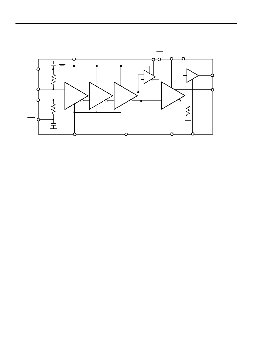
Functional Description
The LG1626DXC is a gallium-arsenide (GaAs) inter-
grated circuit used to provide voltages to drive optical
modulators in high-speed non-return-to-zero (NRZ)
transmission systems. The device is made in a high-
performance 0.9
ç
m gate GaAs hetero-junction FET
technology that utilizes high-density MIM capacitors,
airbridge interconnect, and NiCr film precision resis-
tors. The device contains four cascaded stages,
operates with a single Ù5.2 V power supply, and
accepts ECL 100K level inputs. The output is an
open drain designed to drive 50
loads. Voltages
control the output modulation amplitude and modula-
tor dc offset. A Ù2.5 V band-gap reference is required
for stable operation over temperature and varying
power supply voltage. The LG1626DXC is available
in a 24-lead hermetic, gull-wing package.
5-6549(F)
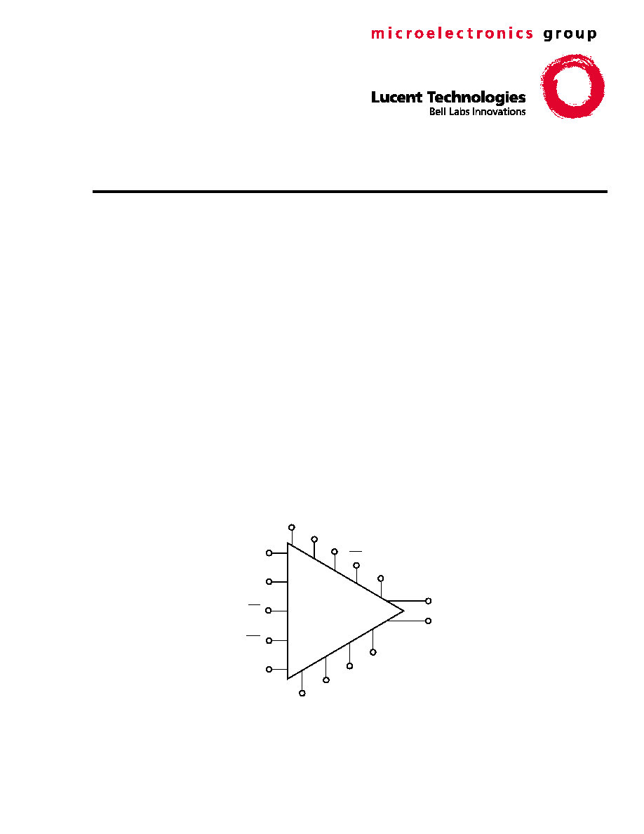
Figure 1. Functional Diagram
V
IN
BG2P5
V
SS1
V
TH
V
SS2
GND
V
OUT
MK
MK
V
SS3
V
MOD
V
OUT-DC
MOD_E
V
IN
V
TH
V
DC-ADJ
2
Lucent Technologies Inc.
Data Sheet
February 1999
LG1626DXC Modulator Driver
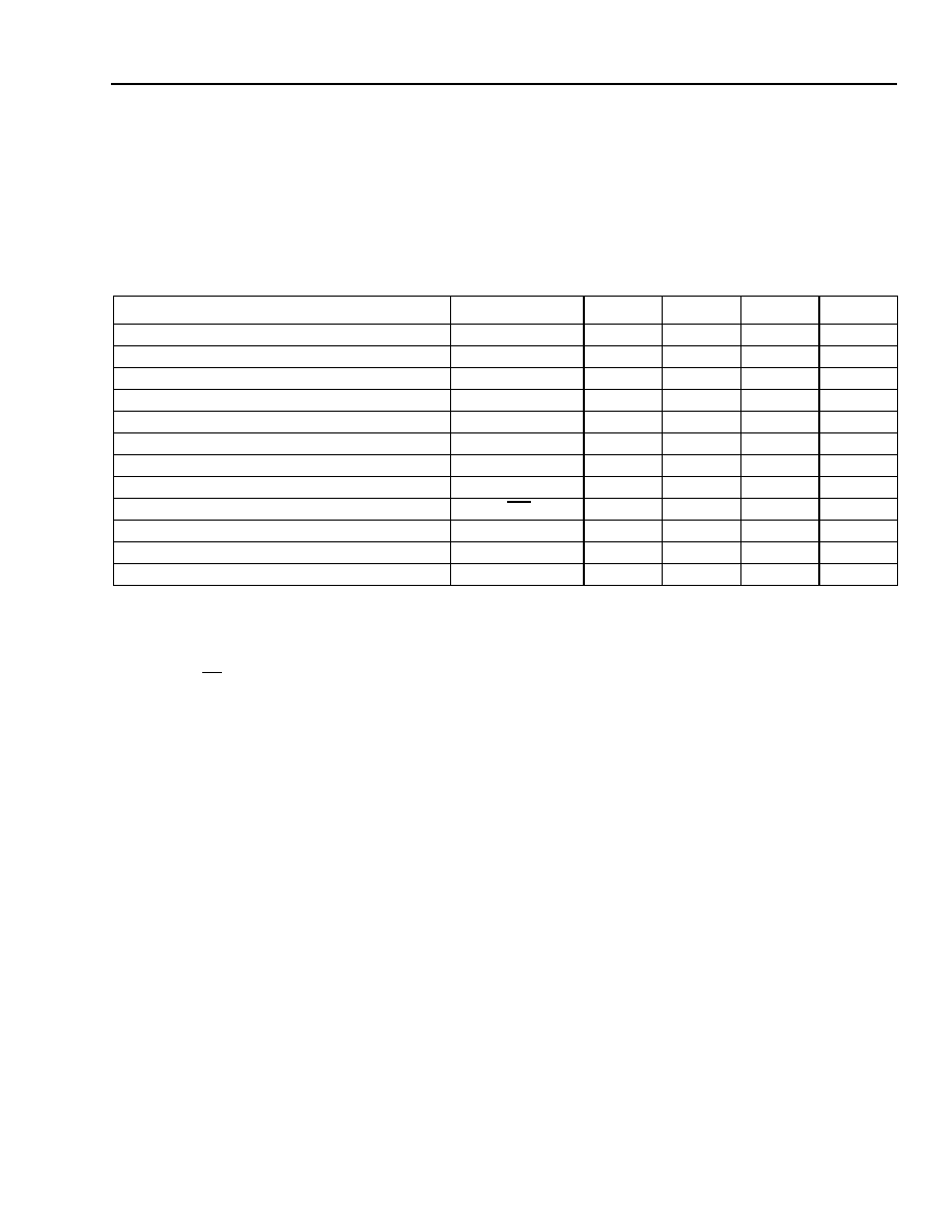
Pin Information
5-6550(F)
Figure 2. LG1626DXC Die Block Diagram
V
TH
V
IN
V
OUT
V
SS3
V
MOD
V
SS1
50
GND
MK
MK
V
SS2
V
DC-ADJ
50
+
Ù
+
Ù
V
IN
V
TH
50
MOD_E

Lucent Technologies Inc.
3
Data Sheet
February 1999
LG1626DXC Modulator Driver
Pin Information
(continued)
5-6551(F)
Note: Figure is not to scale.
Figure 3. LG1626DXC Package Pinout
Table 1. LG1626DXC Pin Description
*
National
Semiconductor
is a registered trademark of National Semiconductor Corporation.
Symbol
Pin
Description
GND
1, 3, 4, 9, 10, 13, 14, 15,
Package Bottom
Ground. For optimum performance, the package bottom must be
soldered to the ground plane.
V
IN
2
Data input.
5
Complementary data input.
6
Complementary threshold control (eye crossing) input.
BG2P5
7
Ù2.5 V band-gap reference (
National
Semiconductor
* LM4040).
MOD_E
8
Modulation enable (connect to V
SS1
to enable, float to disable).
MK
11
Complementary mark density output.
MK
12
Mark density output.
V
OUT
16
Output, ac couple to 50
modulator.
V
OUT-DC
17
Output, modulator dc offset.
V
DC-ADJ
18
Modulator dc offset control input.
V
SS2
19
V
SS2
supply Ù5.2 V for output prebias.
V
SS3
20
V
SS3
supply Ù5.2 V for output modulation.
V
MOD
21
Output modulation control input.
V
SS1
22, 23
V
SS1
supply Ù5.2 V.
V
TH
24
Threshold control (eye crossing) input.
GND
GND
GND
V
OUT
V
OUT-DC
V
DC-ADJ
V
SS2
V
SS3
V
MOD
V
SS1
V
SS1
V
TH
1
2
3
4
5
6
13
14
15
16
17
18
24
BG
2
P
5
MO
D
_
E
GN
D
GN
D
MK
MK
GND
V
IN
GND
GND
V
IN
V
TH
23
22
21
20
19
7
8
9
10
11
12
LG1626DXC
MODULATOR
DRIVER
V
IN
----------
V
TH
-----------

4
Lucent Technologies Inc.
Data Sheet
February 1999
LG1626DXC Modulator Driver
Absolute Maximum Ratings
(at T
A
= 25
¯
C unless otherwise specified)
Table 2. Absolute Maximum Ratings
Handling Precautions
Although protection circuitry has been designed into this device, proper precautions should be taken to avoid expo-
sure to electrostatic discharge (ESD) during handling and mounting. Lucent employs a human-body model (HBM)
and a charged-device model (CDM) for ESD-susceptibility testing and protection design evaluation. ESD voltage
threshold are dependent on the circuit parameters used to define the model. No industry-wide standard has been
adopted for the CDM. However, a standard HBM (resistance = 1500
,
capacitance = 100 pF) is widely used and
therefore, can be used for comparision. The HBM ESD threshold presented here was obtained by using these cir-
cuit parameters.
Table 3. ESD Threshold Voltage
Mounting and Connections
Cetain precautions must be taken when using solder. For installation using a constant temperature solder, temper-
atures of under 300
¯
C may be employed for periods of time up to 5 seconds, maximum. For installation with a sol-
dering iron (battery operated or nonswitching only), the soldering tip temperature should not be greater than
300
¯
C and the soldering time for each lead must not exceed 5 seconds. This device is supplied with solder on the
back of the package. For optimum performance, it is recommended to solder the back of the package to the
ground.
Parameter
Symbol
Min
Max
Unit
Supply Voltage
V
SS
--
5.75
V
Input Voltage
V
I
GND
V
SS
V
Power Dissipation
P
D
--
1
W
Storage Temperature Range
Tstg
Ù40
125
¯
C
Operating Temperature Range
T
C
0
100
¯
C
Human-Body Model ESD Threshold
Device
Voltage
LG1626DXC
>200 V
Lucent Technologies Inc.
5
Data Sheet
February 1999
LG1626DXC Modulator Driver
Electrical Characteristics
T
A
= 25
¯
C, V
SS1
= V
SS2
= V
SS3
= Ù5.2 V, V
TH
= Ù 1.3 V, V
MOD
= Ù 3.8 V, R
L
= 50
.
Minimum and maximum values are testing requirements. Typical values are characteristics of the device and are
the result of engineering evaluations. Typical values are for information purposes only and are not part of the test-
ing requirements. Stresses in excess of the absolute maximum ratings can cause permanent damage to the
device.
Table 4. LG1626DXC Minimum and Maximum Values
1. Maximum output modulation at maximum V
MOD
(R
L
= 50
).
2. Minimum output modulation when MOD_E is floating and V
MOD
= V
SS3.
3. Excludes I
PRE
and average I
MOD:
Power suppy current I
SS2
(relating to prebias) is dependent on V
PRE.
Power suppy current I
SS3
(relating to modulation) is dependent on V
MOD.
4. Both MK and MK are open drains, the typical value is obtained by driving a 1k
load.
5. Maximum modulator dc offset voltage (R
L
= 50
) at maximum V
DC-ADJ.
6. Minimum modulator dc offset voltage (R
L
= 50
) at V
DC-ADJ
= V
SS2.
Note: All parameters measured at 25
¯
C ambient.
Parameter
Symbol
Min
Typ
Max
Unit
Data Input Voltage (peak to peak) Single Ended
V
IN
300
600
1000
mV
Voltage Control for Output Modulation Current
V
MOD
Ù5.5
--
Ù4
V
Maximum Modulated Output Voltage
1
V
OUT
2.70
--
3.00
V
Minimum Modulated Output Voltage
2
V
OUT
0
--
0.2
V
Output Rise and Fall Times (20%--80%)
t
R
, t
F
--
90
--
ps
Power Supply Voltage
V
SS1
, V
SS2
, V
SS3
Ù5.5
Ù5.2
Ù4.9
V
Power Supply Current
3
I
SS1
100
140
180
mA
Mark Density
4
MK
--
Ù0.5
--
V
Complementary Mark Density
4
MK
--
Ù0.5
--
V
Voltage Control for Modulator dc Offset
V
DC-ADJ
Ù5.5
--
Ù3
V
Maximum Output, Modulator dc Offset
5
V
OUT-DC
1.2
--
1.5
V
Minimum Output, Modulator dc Offset
6
V
OUT-DC
0
--
0.1
V
6
Lucent Technologies Inc.
Data Sheet
February 1999
LG1626DXC Modulator Driver
Electrical Characteristics
(continued)
5-6553(F).b
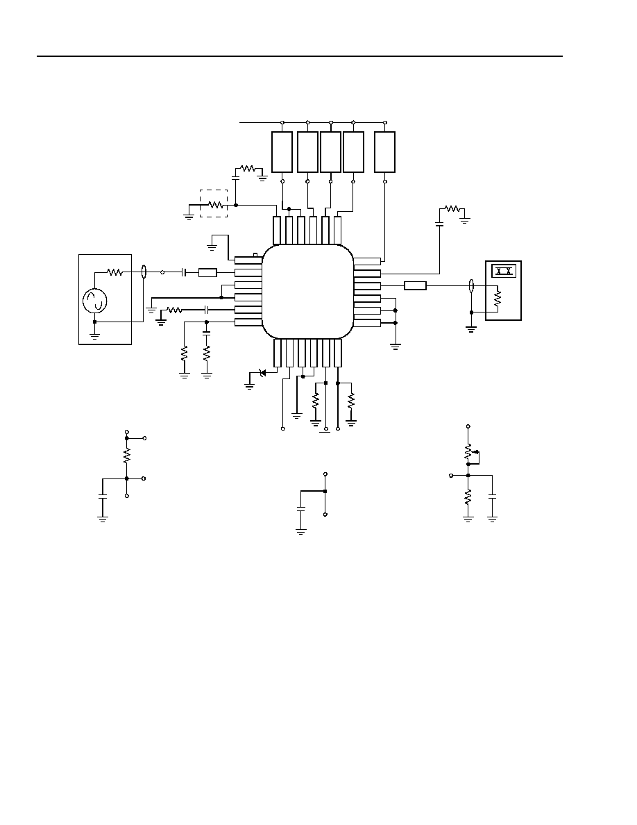
*A 2.5 k
resistor will set the eye crossing at 50%. A 5 k
potentiometer will allow the eye crossing to be varied.
Notes:
All bypass caps should be mounted close to the package.
I
SS3
can be measured and used to control V
MOD
.
I
SS2
can be measured and used to control V
OUT-DC
.
For optimal performance, the proximity of the two components should be minimized and the package bottom must be soldered to the circuit
board (GND).
For proper impedance matching, high-speed transmission lines should be 50
controlled impedance lines.
Figure 4. LG1626DXC Typical Electrical Evaluation (ac Coupled to Scope)
VO
L
T
A
G
E
DI
VI
DER
CURR
ENT
SENSE
V
SS1
BYPASS
1
2
3
4
5
6
7
8
9 10 11 12
13
14
15
16
17
18
19
20
21
22
23
24
LG1626DXC
MODULATOR
DRIVER
50
50
+
DATA
GENERATOR
SCOPE
Zo = 50
DATA IN
V
SS
1
V
SS
3
V
MO
D
2.5 k
*
V
SS
= Ù5.2 V
0.047
ç
F
1 k
1 k
MK MK
1
3 k
2 k
V
SS
0.1
ç
F
REQUIRED TO SET
V
MOD
AND V
DC-ADJ
TO ACHIEVE DESIRED
MODULATION, ONE EACH.
VOLTAGE
DIVIDER
V
SS
0.1
ç
F
TO USER-SUPPLIED
VOLTAGE MONITOR
TO NODE
V
SS2
AND V
SS3
(DVM).
CURRENT
SENSE
ONE EACH.
0.1
ç
F
V
SS
BYPASS
FOR V
SS1
V
SS1
V
TH
V
IN
V
OUT
V
SS
2
V
OUT-DC
V
DC-
A
D
J
VO
L
T
A
G
E
DI
VI
DER
CURR
ENT
SENSE
Zo = 50
0.1
ç
F
10
0.1
ç
F
BG2P5
LM4040
MOD_5
V
SS
= Ù5.2 V
10
0.047
ç
F
2.5 k
10
0.1
ç
F
50
Lucent Technologies Inc.
7
Data Sheet
February 1999
LG1626DXC Modulator Driver
Electrical Characteristics
(continued)
5-6554(F).b
*A 2.5 k
resistor will set the eye crossing at 50%. A 5 k
potentiometer will allow the eye crossing to be varied.
Notes:
All bypass caps should be mounted close to the package.
I
SS3
can be measured and used to control V
MOD
.
I
SS2
can be measured and used to control V
OUT-DC
.
For optimal performance, the proximity of the two components should be minimized and the package bottom must be soldered to the circuit
board (GND).
For proper impedance matching, high-speed transmission lines should be 50
controlled impedance lines.
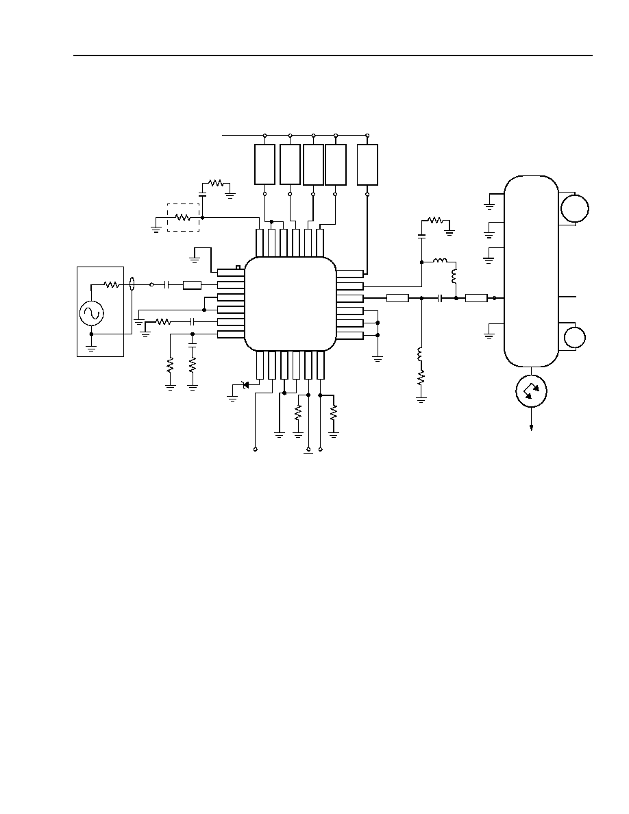
Figure 5. Typical Optical Evaluation of the LG1626DXC and EM2500 EM-ILM
VO
L
T
AG
E
DIVI
DER
CU
RRENT
SENSE
VSS1
BYPASS
VSS1
VSS3
VM
O
D
VTH
VS
S2
CU
RRE
NT
SENSE
1
2
3
4
5
6
7
8
9
10 11 12
13
14
15
16
17
18
19
20
21
22
23
24
LG1626DXC
MODULATOR
DRIVER
Zo = 50
Zo = 50
DATA
2.5 k
*
0.1
ç
F
VSS = Ù5.2 V
0.047
ç
F
1 k
1 k
MK MK
VIN
VOUT
VOUT-DC
V
DC-
A
D
J
VO
L
T
AG
E
DIVI
DER
Zo = 50
1
2
3
4
5
6
7
14
13
12
11
10
9
8
E2500
EM-ILM
INPUT
+2 V
MAX
DMM
dc
SUPPLY
0.1
ç
F
IN
VSS = Ù5.2 V
MOD_E
BG2P5
LM4040
50
+
DATA
GENERATOR
0.047
ç
F
2.5 k
10
0.1
ç
F
10
10
50
50
0.047
ç
F
10
ç
H
10
ç
H
100
ç
H

8
Lucent Technologies Inc.
Data Sheet
February 1999
LG1626DXC Modulator Driver
Electrical Characteristics
(continued)
5-7341(F)
Figure 6. Typical Electrical Eye Diagram (ac Coupled to Scope)
5-7342(F)
Figure 7. Typical Optical Eye Diagram
Table 5. Pin Description of Lucent's E2500 EM-ILM Modulator
Pin
Description
1, 2
Thermistor
3
Laser Anode
4
Monitor Anode
5
Monitor Cathode
6
Thermoelectric Cooler (+)
7
Thermoelectric Cooler (Ù)
8, 9
Case Ground
10, 14 No Connect
11, 13 Laser/Modulator Ground
12
Modulator Anode (Ù) 50
RF Input
750
mV
/
d
i
v
80 ps/div
500 m
W
/
div
60 ps/div
Lucent Technologies Inc.
9
Data Sheet
February 1999
LG1626DXC Modulator Driver
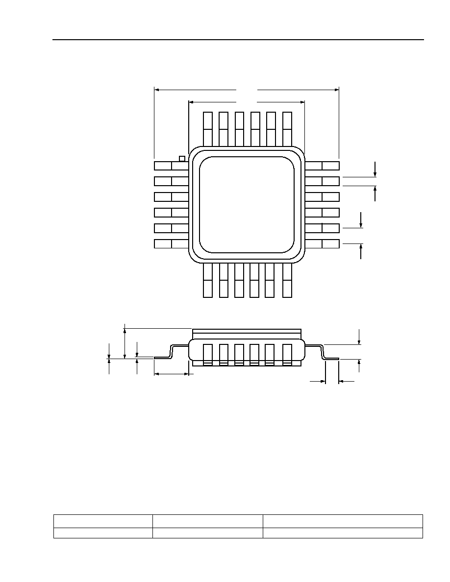
Outline Diagram
12-3224(F).a
Assembly Notes:
Standoff specifications applies to package prior to solder dipping of leads and package base.
During board assembly use back lighting to silhouette the package. This will eliminate reflection problems with the
solder on the bottom of the package.
Lead space tolerance should be set to
Ý
0.012 in.
Board solder pattern for the package base should not exceed 50% of the package base area.
Insertion pressure should not exceed 125 grams.
LG1626DXC Ordering Information
Device
Type
Comcode Number
LG1626DXC
24-Pin Package
108192865
1
1
0 -- 0.004
0.082
0.005
0.092
0.045
0.035
0.030
0.012
0.280
0.465
LUCENT
LG1626DXC
XXXXXXX

Lucent Technologies Inc. reserves the right to make changes to the product(s) or information contained herein without notice. No liability is assumed as a result of their use or application. No
rights under any patent accompany the sale of any such product(s) or information.
Copyright ˋ 1999 Lucent Technologies Inc.
All Rights Reserved
February 1999
DS99-145HSPL
For additional information, contact your Microelectronics Group Account Manager or the following:
INTERNET:
http://www.lucent.com/micro
E-MAIL:
docmaster@micro.lucent.com
N. AMERICA:
Microelectronics Group, Lucent Technologies Inc., 555 Union Boulevard, Room 30L-15P-BA, Allentown, PA 18103
1-800-372-2447, FAX 610-712-4106 (In CANADA: 1-800-553-2448, FAX 610-712-4106)
ASIA PACIFIC: Microelectronics Group, Lucent Technologies Singapore Pte. Ltd., 77 Science Park Drive, #03-18 Cintech III, Singapore 118256
Tel. (65) 778 8833, FAX (65) 777 7495
CHINA:
Microelectronics Group, Lucent Technologies (China) Co., Ltd., A-F2, 23/F, Zao Fong Universe Building, 1800 Zhong Shan Xi Road, Shanghai
200233 P. R. China Tel. (86) 21 6440 0468, ext. 316, FAX (86) 21 6440 0652
JAPAN:
Microelectronics Group, Lucent Technologies Japan Ltd., 7-18, Higashi-Gotanda 2-chome, Shinagawa-ku, Tokyo 141, Japan
Tel. (81) 3 5421 1600, FAX (81) 3 5421 1700
EUROPE:
Data Requests: MICROELECTRONICS GROUP DATALINE: Tel. (44) 1189 324 299, FAX (44) 1189 328 148
Technical Inquiries:GERMANY: (49) 89 95086 0 (Munich), UNITED KINGDOM: (44) 1344 865 900 (Ascot),
FRANCE: (33) 1 40 83 68 00 (Paris), SWEDEN: (46) 8 594 607 00 (Stockholm), FINLAND: (358) 9 4354 2800 (Helsinki),
ITALY: (39) 02 6608131 (Milan), SPAIN: (34) 1 807 1441 (Madrid)