SRF4427
SRF4427G
Advanced Power Technology reserves the right to change, without notice, the specifications and information contained herein
Visit our website at WWW.ADVANCEDPOWER.COM or contact our factory direct.
Rev A 9/2005
* G Denotes RoHS Compliant, Pb Free Terminal Finish
DESCRIPTION:
Designed for general-purpose RF amplifier applications, such as pre-drivers and oscillators.
ABSOLUTE MAXIMUM RATINGS (Tcase = 25
°
C)
Symbol
Parameter
Value Unit
V
CEO
Collector-Emitter
Voltage
18 Vdc
V
CBO
Collector-Base
Voltage
36 Vdc
V
EBO
Emitter-Base Voltage
4.0 Vdc
I
C
Collector
Current
400 mA
Thermal Data
P
D
Total Device Dissipation @ TC = 25şC
Derate above 25şC
1.5
12.5
Watts
mW/ şC
T
STG
Storage Temperature
-65
to
+
150
şC
R
JA
Thermal Resistance, Junction to Ambient
125
şC/W
Features
·
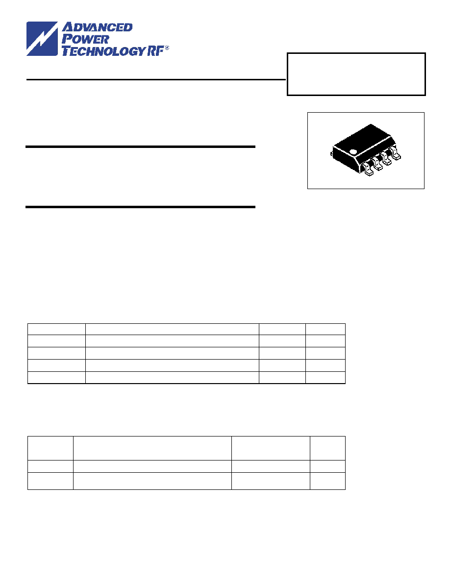
Low Cost SO-8 Plastic Surface Mount Package.
·
S-Parameter Characterization
·
Tape and Reel Packaging Options Available
·
Maximum Available Gain 20dB(typ) @ 200MHz
RF AND MICROWAVE DISCRETE LOW
POWER TRANSISTORS
GENERAL RF AMPLIFIER APPLICATIONS
140 COMMERCE DRIVE
MONTGOMERYVILLE, PA
18936-1013
PHONE: (215) 631-9840
FAX: (215) 631-9855
SRF4427
SRF4427G
Advanced Power Technology reserves the right to change, without notice, the specifications and information contained herein
Visit our website at WWW.ADVANCEDPOWER.COM or contact our factory direct.
Rev A 9/2005
ELECTRICAL SPECIFICATIONS (Tcase = 25
°
C)
STATIC (off)
Value
Symbol
Test Conditions
Min. Typ. Max.
Units
BV
CEO
Collector-Emitter Breakdown Voltage
(IC = 10 mAdc, IB = 0)
18
-
-
Vdc
BV
CES
Collector-Base Breakdown Voltage
(IC = 5 mAdc, IE = 0)
36
-
-
Vdc
BV
EBO
Emitter-Base Breakdown Voltage
(IE = 5 mAdc, IC = 0)
4
-
-
Vdc
I
CBO
Collector Cutoff Current
(VCB = 12.5 Vdc)
-
-
800
uA
STATIC (on)
Value
Symbol
Test Conditions
Min. Typ. Max.
Units
HFE
DC Current Gain
(VCE = 5 Vdc, IC = 150 mAdc)
20
200
DYNAMIC
Value
Symbol
Test Conditions
Min. Typ. Max.
Units
F
TAU
Current-Gain Bandwidth Product
(IC = 50 mAdc, VCE = 12 Vdc, f = 200 MHz)
1.3
GHz
C
OB
Output Capacitance
(VCB = 12 Vdc, IE = 0, f = 1.0 MHz)
3.4
GHz
FUNCTIONAL
Value
Symbol
Test Conditions
Min. Typ. Max.
Unit
G
PE
Power Gain
VCE = 12 Vdc, f = 175 MHz, Pin = 15 mW
17
18
-
dB
|S
21
|
2
Insertion Gain
VCE = 12 Vdc , IC = 50 mAdc, f = 200 MHz
12
14
-
dB

SRF4427
SRF4427G
Advanced Power Technology reserves the right to change, without notice, the specifications and information contained herein
Visit our website at WWW.ADVANCEDPOWER.COM or contact our factory direct.
Rev A 9/2005
PACKAGE MECHANICAL DATA
1.
4.
8.
5.
PIN 1. EMITTER
2. COLLECTOR
3. COLLECTOR
4. EMITTER
5. EMITTER
6. BASE
7. BASE
8. EMITTER