APTM100UM65D-AlN
A
P
T
M
100U
M
65D
-
A
l
N
ş
R
e
v 0 J
u
l
y, 2004
APT website ş http://www.advancedpower.com
1 ş 6
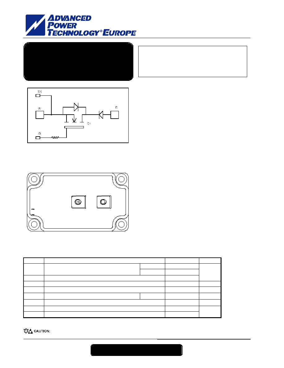
D
S
G
SK
Absolute maximum ratings
These Devices are sensitive to Electrostatic Discharge. Proper Handing Procedures Should Be Followed.
Symbol Parameter
Max ratings
Unit
V
DSS
Drain - Source Breakdown Voltage
1000
V
T
c
= 25░C
145
I
D
Continuous
Drain
Current
T
c
= 80░C
110
I
DM
Pulsed Drain current
580
A
V
GS
Gate - Source Voltage
▒30
V
R
DSon
Drain - Source ON Resistance
65
m
P
D
Maximum Power Dissipation
T
c
= 25░C
3250
W
I
AR
Avalanche current (repetitive and non repetitive)
30
A
E
AR
Repetitive Avalanche Energy
50
E
AS
Single Pulse Avalanche Energy
3200
mJ
V
DSS
= 1000V
R
DSon
= 65m max @ Tj = 25░C
I
D
= 145A @ Tc = 25░C
Application
Ě Zero Current Switching resonant mode
Features
Ě Power MOS 7
«
MOSFETs
- Low R
DSon
- Low input and Miller capacitance
- Low gate charge
- Avalanche energy rated
- Very rugged
Ě Kelvin source for easy drive
Ě Very low stray inductance
- Symmetrical design
- M5 power connectors
Ě High level of integration
Ě AlN substrate for improved thermal performance
Benefits
Ě Outstanding performance at high frequency
operation
Ě Direct mounting to heatsink (isolated package)
Ě Low junction to case thermal resistance
Ě Low profile
Single switch
with Series diode
MOSFET Power Module
APTM100UM65D-AlN
A
P
T
M
100U
M
65D
-
A
l
N
ş
R
e
v 0 J
u
l
y, 2004
APT website ş http://www.advancedpower.com
2 ş 6
All ratings @ T
j
= 25░C unless otherwise specified
Electrical Characteristics
Symbol Characteristic
Test
Conditions
Min Typ Max Unit
BV
DSS
Drain - Source Breakdown Voltage
V
GS
= 0V, I
D
= 1mA
1000
V
V
GS
= 0V,V
DS
= 1000V
T
j
= 25░C
400
ÁA
I
DSS
Zero Gate Voltage Drain Current
V
GS
= 0V,V
DS
= 800V
T
j
= 125░C
2
mA
R
DS(on)
Drain ş Source on Resistance
V
GS
= 10V, I
D
= 75A
65
m
V
GS(th)
Gate
Threshold
Voltage
V
GS
= V
DS
, I
D
=
20mA
3 5 V
I
GSS
Gate ş Source Leakage Current
V
GS
= ▒30 V, V
DS
= 0V
▒400
nA
Dynamic Characteristics
Symbol Characteristic
Test
Conditions
Min Typ Max Unit
C
iss
Input
Capacitance
28.5
C
oss
Output
Capacitance
5.08
C
rss
Reverse Transfer Capacitance
V
GS
= 0V
V
DS
= 25V
f = 1MHz
0.9
nF
Q
g
Total gate Charge
1068
Q
gs
Gate ş Source Charge
136
Q
gd
Gate ş Drain Charge
V
GS
= 10V
V
Bus
= 500V
I
D
= 145A
692
nC
T
d(on)
Turn-on
Delay
Time
18
T
r
Rise Time
14
T
d(off)
Turn-off Delay Time
140
T
f
Fall Time
V
GS
= 15V
V
Bus
= 500V
I
D
= 145A
R
G
= 0.75
55
ns
E
on
Turn-on Switching Energy
4.8
E
off
Turn-off Switching Energy
Inductive switching @ 25░C
V
GS
= 15V, V
Bus
= 670V
I
D
= 145A,
R
G
= 0.75
2.9
mJ
E
on
Turn-on Switching Energy
8
E
off
Turn-off Switching Energy
Inductive switching @ 125░C
V
GS
= 15V, V
Bus
= 670V
I
D
= 145A,
R
G
= 0.75
3.9
mJ
E
on
includes diode reverse recovery.
In accordance with JEDEC standard JESD24-1.
Series diode ratings and characteristics
Symbol Characteristic
Test
Conditions
Min Typ Max Unit
V
RRM
Maximum Repetitive Reverse Voltage
1000 V
I
RM
Maximum Reverse Leakage Current
V
R
=1000V
T
j
= 125░C
2
mA
I
F(A V)
Maximum Average Forward Current 50% duty cycle
T
c
= 100░C
240 A
I
F
= 240A
1.9
2.5
I
F
= 480A
2.2
V
F
Diode Forward Voltage
I
F
= 240A
T
j
= 125░C
1.7
V
T
j
= 25░C
280
t
rr
Reverse Recovery Time
I
F
= 240A
V
R
= 667V
di/dt = 800A/Ás
T
j
= 125░C
350
ns
T
j
= 25░C
3
Q
rr
Reverse Recovery Charge
I
F
= 240A
V
R
= 667V
di/dt = 800A/Ás
T
j
= 125░C
14.4
ÁC
APTM100UM65D-AlN
A
P
T
M
100U
M
65D
-
A
l
N
ş
R
e
v 0 J
u
l
y, 2004
APT website ş http://www.advancedpower.com
3 ş 6
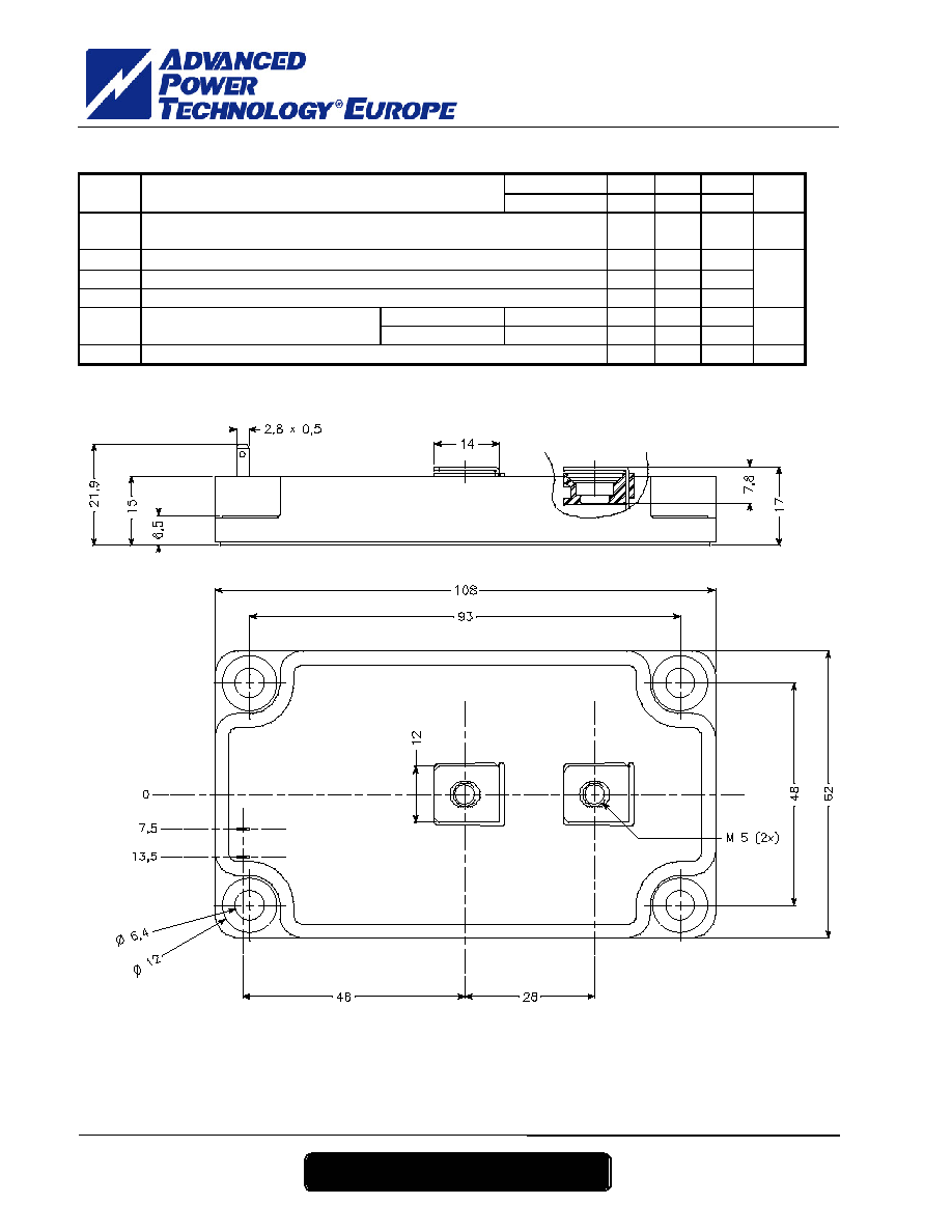
Thermal and package characteristics
Symbol Characteristic
Min Typ Max Unit
Transistor
0.038
R
thJC
Junction
to
Case
Series diode
0.23
░C/W
V
ISOL
RMS Isolation Voltage, any terminal to case t =1 min,
I isol<1mA, 50/60Hz
2500
V
T
J
Operating junction temperature range
-40 150
T
STG
Storage Temperature Range
-40
125
T
C
Operating Case Temperature
-40
100
░C
To Heatsink
M6
3
5
Torque Mounting
torque
For teminals
M5
2
3.5
N.m
Wt Package
Weight
280 g
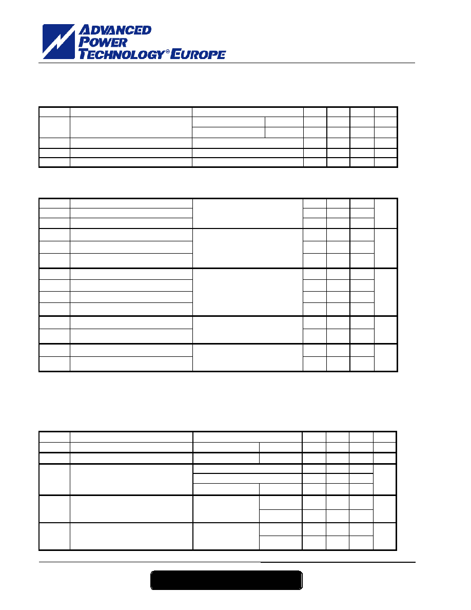
Package outline
APTM100UM65D-AlN
A
P
T
M
100U
M
65D
-
A
l
N
ş
R
e
v 0 J
u
l
y, 2004
APT website ş http://www.advancedpower.com
4 ş 6
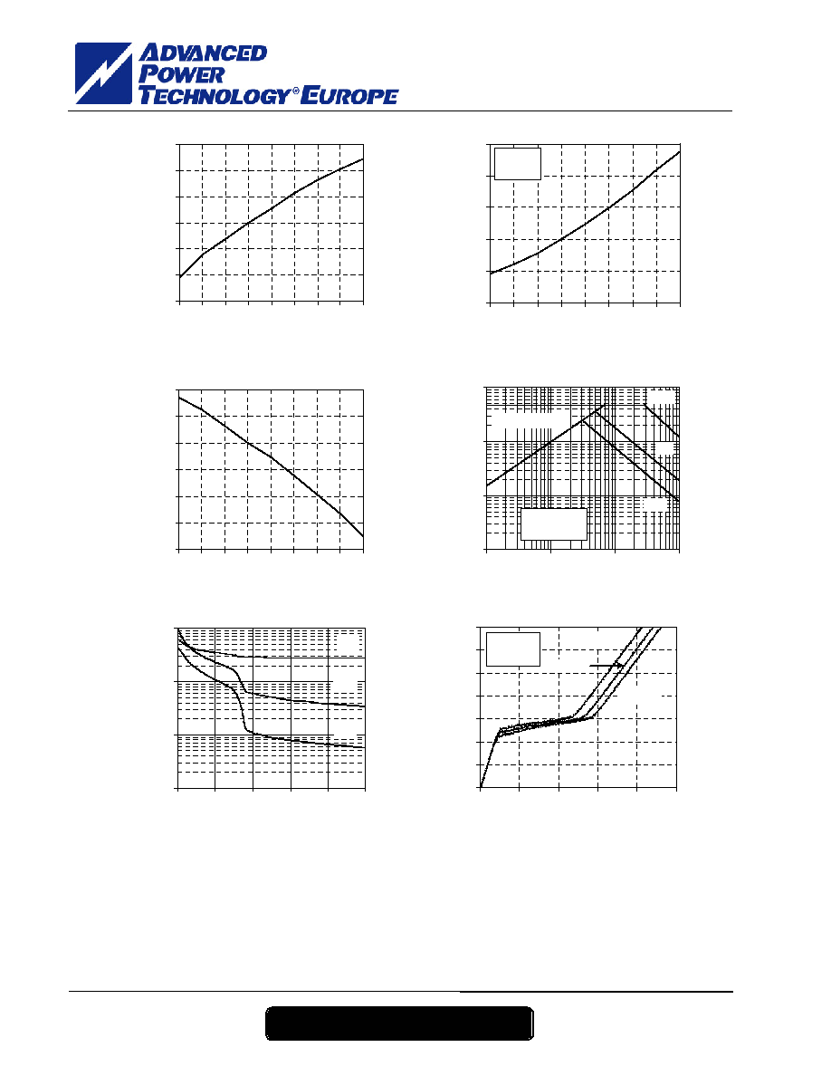
Typical Performance Curve
0.9
0.7
0.5
0.3
0.1
0.05
Single Pulse
0
0.005
0.01
0.015
0.02
0.025
0.03
0.035
0.04
0.00001
0.0001
0.001
0.01
0.1
1
10
rectangular Pulse Duration (Seconds)
The
r
m
a
l
I
m
pe
da
nc
e
(
░
C
/
W
)
Maximum Effective Transient Thermal Impedance, Junction to Case vs Pulse Duration
5V
5.5V
6V
6.5V
7V
0
40
80
120
160
200
240
280
320
360
0
5
10
15
20
25
30
V
DS
, Drain to Source Voltage (V)
I
D
,
Dr
a
i
n
Cu
r
r
e
n
t
(
A
)
V
GS
=15, 10V
Low Voltage Output Characteristics
Transfert Characteristics
T
J
=-55░C
T
J
=25░C
T
J
=125░C
0
80
160
240
320
400
480
0
1
2
3
4
5
6
7
8
V
GS
, Gate to Source Voltage (V)
I
D
,
Dr
a
i
n
Cu
r
r
e
n
t
(
A
)
V
DS
> I
D
(on)xR
DS
(on)MAX
250Ás pulse test @ < 0.5 duty cycle
R
DS(on)
vs Drain Current
V
GS
=10V
V
GS
=20V
0.8
0.9
1
1.1
1.2
1.3
1.4
0
80
160
240
320
I
D
, Drain Current (A)
R
DS
(
o
n
)
D
r
ai
n
t
o
S
o
u
r
ce O
N
R
e
si
st
an
ce
Normalized to
V
GS
=10V @ 72.5A
0
40
80
120
160
25
50
75
100
125
150
T
C
, Case Temperature (░C)
I
D
,
DC
D
r
a
i
n
Cu
r
r
e
n
t
(
A
)
DC Drain Current vs Case Temperature
APTM100UM65D-AlN
A
P
T
M
100U
M
65D
-
A
l
N
ş
R
e
v 0 J
u
l
y, 2004
APT website ş http://www.advancedpower.com
5 ş 6
0.85
0.90
0.95
1.00
1.05
1.10
1.15
-50 -25
0
25 50 75 100 125 150
T
J
, Junction Temperature (░C)
BV
DS
S
,
D
r
ai
n
t
o
S
o
u
r
ce
B
r
eak
d
o
w
n
V
o
l
t
ag
e (
N
o
r
m
a
l
i
z
e
d
)
Breakdown Voltage vs Temperature
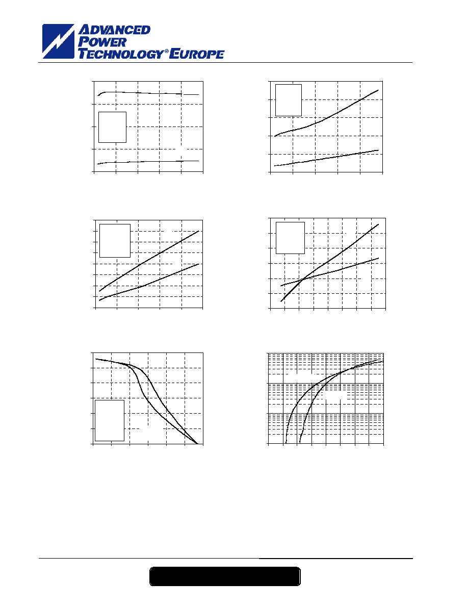
ON resistance vs Temperature
0.0
0.5
1.0
1.5
2.0
2.5
-50 -25
0
25 50 75 100 125 150
T
J
, Junction Temperature (░C)
R
DS
(
o
n
)
,
D
r
a
i
n
t
o
S
o
u
r
ce O
N
r
esi
st
an
ce
(
N
or
m
a
l
i
z
e
d)
V
GS
=10V
I
D
=72.5A
Threshold Voltage vs Temperature
0.6
0.7
0.8
0.9
1.0
1.1
1.2
-50 -25
0
25 50 75 100 125 150
T
C
, Case Temperature (░C)
V
GS
(
T
H
)
,
Th
r
e
s
hol
d
V
o
l
t
a
g
e
(N
o
r
ma
l
i
z
e
d
)
Maximum Safe Operating Area
10ms
1ms
100Ás
1
10
100
1000
1
10
100
1000
V
DS
, Drain to Source Voltage (V)
I
D
,
Dr
a
i
n
Cu
r
r
e
n
t
(
A
)
limited by R
DS
on
Single pulse
T
J
=150░C
Ciss
Crss
Coss
100
1000
10000
100000
0
10
20
30
40
50
V
DS
, Drain to Source Voltage (V)
C
,
C
a
p
aci
t
a
n
ce (
p
F
)
Capacitance vs Drain to Source Voltage
V
DS
=200V
V
DS
=500V
V
DS
=800V
0
2
4
6
8
10
12
14
0
300
600
900
1200
1500
Gate Charge (nC)
V
GS
,
G
a
t
e
t
o
S
o
u
r
ce V
o
l
t
ag
e
(
V
)
Gate Charge vs Gate to Source Voltage
I
D
=145A
T
J
=25░C
APTM100UM65D-AlN
A
P
T
M
100U
M
65D
-
A
l
N
ş
R
e
v 0 J
u
l
y, 2004
APT website ş http://www.advancedpower.com
6 ş 6
Delay Times vs Current
t
d(on)
t
d(off)
0
40
80
120
160
50
94
138
182
226
270
I
D
, Drain Current (A)
t
d(o
n
)
a
nd t
d(
off
)
(n
s
)
V
DS
=670V
R
G
=0.75
T
J
=125░C
L=100ÁH
Rise and Fall times vs Current
t
r
t
f
0
20
40
60
80
100
50
94
138
182
226
270
I
D
, Drain Current (A)
t
r
an
d
t
f
(n
s
)
V
DS
=670V
R
G
=0.75
T
J
=125░C
L=100ÁH
Switching Energy vs Current
E
on
E
off
0
2
4
6
8
10
12
14
16
50
94
138
182
226
270
I
D
, Drain Current (A)
S
w
i
t
ch
i
n
g
E
n
er
g
y
(
m
J)
V
DS
=670V
R
G
=0.75
T
J
=125░C
L=100ÁH
E
on
E
off
2
6
10
14
18
22
26
0
1
2
3
4
5
6
7
8
Gate Resistance (Ohms)
S
w
it
c
h
in
g
E
n
e
r
g
y
(
m
J
)
Switching Energy vs Gate Resistance
V
DS
=670V
I
D
=145A
T
J
=125░C
L=100ÁH
Hard
switching
ZCS
0
50
100
150
200
250
300
15
35
55
75
95
115
135
I
D
, Drain Current (A)
F
r
eq
u
e
n
cy (
k
H
z
)
Operating Frequency vs Drain Current
V
DS
=670V
D=50%
R
G
=0.75
T
J
=125░C
T
C
=75░C
T
J
=25░C
T
J
=150░C
1
10
100
1000
0.2 0.4 0.6 0.8
1
1.2 1.4 1.6 1.8
V
SD
, Source to Drain Voltage (V)
I
DR
,
R
ever
se D
r
ai
n
C
u
r
r
e
n
t
(
A
)
Source to Drain Diode Forward Voltage
APT reserves the right to change, without notice, the specifications and information contained herein
APT's products are covered by one or more of U.S patents 4,895,810 5,045,903 5,089,434 5,182,234 5,019,522
5,262,336 6,503,786 5,256,583 4,748,103 5,283,202 5,231,474 5,434,095 5,528,058 and foreign patents. U.S and Foreign patents pending. All Rights Reserved.