
JPEG2000 Video Codec
ADV202
Rev. 0
Information furnished by Analog Devices is believed to be accurate and reliable.
However, no responsibility is assumed by Analog Devices for its use, nor for any
infringements of patents or other rights of third parties that may result from its use.
Specifications subject to change without notice. No license is granted by implication
or otherwise under any patent or patent rights of Analog Devices. Trademarks and
registered trademarks are the property of their respective owners.
One Technology Way, P.O. Box 9106, Norwood, MA 02062-9106, U.S.A.
Tel: 781.329.4700
www.analog.com
Fax: 781.326.8703
© 2004 Analog Devices, Inc. All rights reserved.
FEATURES
Complete single-chip JPEG2000 compression and
decompression solution for video and still images
Patented SURFTM (spatial ultraefficient recursive filtering)
technology enables low power and low cost wavelet based
compression
Supports both 9/7 and 5/3 wavelet transforms with up to
6 levels of transform
Programmable tile/image size with widths up to 2048 pixels
in 3-component 4:2:2 interleaved mode, and up to
4096 pixels in single-component mode
Maximum tile/image height: 4096 pixels
Video interface directly supporting ITU.R-BT656,
SMPTE125M PAL/ NTSC, SMPTE274M, SMPTE293M (525p),
ITU.R-BT1358 (625p) or any video format with a maximum
input rate of 65 MSPS for irreversible mode or 40 MSPS for
reversible mode
Two or more ADV202s can be combined to support full-
frame SMPTE274M HDTV (1080i) or SMPTE296M (720p)
Interlaces temporally coherent frame-based SD video
sources for improved performance
Flexible asynchronous SRAM-style host interface allows
glueless connection to most 16-/32-bit microcontrollers
and ASICs
2.5 V to 3.3 V I/O and 1.5 V core supply
12 mm × 12 mm 121-lead CSPBGA, speed grade 115 MHz, or
13 mm × 13 mm 144-lead CSPBGA, speed grade 150 MHz
APPLICATIONS
Networked video and image distribution systems
Wireless video and image distribution
Image archival/retrieval
Digital CCTV and surveillance systems
Digital cinema systems
Professional video editing and recording
Digital still cameras
Digital camcorders
GENERAL DESCRIPTION
The ADV202 is a single-chip JPEG2000 codec targeted for
video and high bandwidth image compression applications that
can benefit from the enhanced quality and feature set provided
by the JPEG2000 (J2K)--ISO/IEC15444-1 image compression
standard. The part implements the computationally intensive
operations of the JPEG2000 image compression standard as
well as providing fully compliant code-stream generation for
most applications.
The ADV202's dedicated video port provides glueless
connection to common digital video standards such as ITU.R-
BT656, SMPTE125M, SMPTE293M [525p], ITU.R-BT1358
[625p], SMPTE274M[1080i], or SMPTE296M[720p]. A variety
of other high speed synchronous pixel and video formats can
also be supported using the programmable framing and
validation signals.
(continued on Page 3)
FUNCTIONAL BLOCK DIAGRAM
04723-001
WAVELET
ENGINE
EC1
EC2
EC3
INTERNAL BUS AND DMA ENGINE
EMBEDDED RISC
PROCESSOR
SYSTEM
MEMORY
SYSTEM
ANCILLARY
FIFO
PIXEL I/F
EXTERNAL
DMA CTRL
PIXEL
FIFO
CODE
FIFO
ATTRIBUTE
FIFO
PIXEL I/F
HOST I/F
ADV202
Figure 1.

ADV202
Rev. 0 | Page 2 of 40
TABLE OF CONTENTS
General Description ......................................................................... 3
JPEG2000 Feature Support.......................................................... 3
Specificatons...................................................................................... 4
Supply Voltages and Current....................................................... 4
Input/Output Specifications........................................................ 4
Clock and RESET Specifications ................................................ 5
Normal Host Mode--Read Operation ...................................... 6
Normal Host Mode--Write Operation ..................................... 7
DREQ/DACK DMA Mode--Single FIFO Write Operation .. 8
DREQ/DACK DMA Mode--Single FIFO Read Operation . 10
External DMA Mode--FIFO Write, Burst Mode................... 12
External DMA Mode--FIFO Read, Burst Mode.................... 13
Streaming Mode (JDATA)--FIFO Read/Write ...................... 15
VDATA Mode Timing ............................................................... 15
Raw Pixel Mode Timing ............................................................ 17
SPI Port Timing .......................................................................... 18
Pin BGA Assignments and Function Descriptions.................... 19
Pin BGA Assignments ............................................................... 19
Pin Function Descriptions ........................................................ 22
Theory of Operation ...................................................................... 25
Wavelet Engine ........................................................................... 25
Entropy Codecs........................................................................... 25
Embedded Processor System .................................................... 25
Memory System .......................................................................... 25
Internal DMA Engine ................................................................ 25
ADV202 Interface........................................................................... 26
Video Interface (VDATA Bus).................................................. 26
Host Interface (HDATA Bus) ................................................... 26
Direct and Indirect Registers .................................................... 26
Control Access Registers ........................................................... 27
Pin Configuration and Bus Sizes/Modes ................................ 27
Stage Register .............................................................................. 27
JDATA Mode............................................................................... 27
External DMA Engine ............................................................... 27
SPI Port ........................................................................................ 27
Internal Registers............................................................................ 28
Direct Registers........................................................................... 28
Indirect Registers........................................................................ 29
PLL ............................................................................................... 30
Hardware Boot............................................................................ 31
Video Input Formats ...................................................................... 32
Applications..................................................................................... 34
Encode--Multichip Mode......................................................... 34
Decode--Multichip Master/Slave ............................................ 35
Digital Still Camera/Camcorder .............................................. 35
Encode/Decode SDTV Video Application.............................. 36
ASIC Application (32-Bit Host/32-Bit ASIC) ......................... 37
HIPI (Host Interface--Pixel Interface) ................................... 38
JDATA Interface ......................................................................... 38
Outline Dimensions ....................................................................... 39
Ordering Guide .......................................................................... 40
REVISION HISTORY
7/04--Revision 0: Initial Version

ADV202
Rev. 0 | Page 3 of 40
GENERAL DESCRIPTION
(continued from Page 1)
The ADV202 can process images at a rate of 40MSPS in
reversible mode and at higher rates when used in irreversible
mode. The ADV202 contains a dedicated wavelet transform
engine, three entropy codecs, an on-board memory system, and
an embedded RISC processor that can provide a complete
JPEG2000 compression/decompression solution.
The wavelet processor supports the 9/7 irreversible wavelet
transform and the 5/3 wavelet transform in reversible and
irreversible modes. The entropy codecs support all features in
the JPEG2000 Part 1 specification, except Maxshift ROI.
The ADV202 operates on a rectangular array of pixel samples
called a tile. A tile can contain a complete image, up to the
maximum supported size, or some portion of an image. The
maximum horizontal tile size supported depends on the wavelet
transform selected and the number of samples in the tile.
Images larger than the ADV202's maximum tile size can be
broken into individual tiles and then sent sequentially to the
chip while still maintaining a single, fully compliant JPEG2000
code stream for the entire image.
JPEG2000 FEATURE SUPPORT
The ADV202 supports a broad set of features that are included
in Part 1 of the JPEG2000 standard (ISO/IEC 15444). See
Getting Started with ADV202 for information on the JPEG2000
features that the ADV202 currently supports.
Depending on the particular application requirements, the
ADV202 can provide varying levels of JPEG2000 compression
support. It can provide raw code-block and attribute data
output, which allows the host software to have complete control
over the generation of the JPEG2000 code stream and other
aspects of the compression process such as bit-rate control.
Otherwise, the ADV202 can create a complete, fully compliant
JPEG2000 code stream (.j2c) and enhanced file formats such as
.jp2, .jpx, and .mj2 (Motion JPEG2000). See Getting Started with
ADV202 for information on the formats that the ADV202
currently supports.

ADV202
Rev. 0 | Page 4 of 40
SPECIFICATONS
SUPPLY VOLTAGES AND CURRENT
Table 1.
Parameter
Description
Min
Typ
Max
Unit
VDD
DC Supply Voltage, Core
1.425
1.5
1.575
V
IOVDD
DC Supply Voltage, I/O
2.375
3.3
3.63
V
PLLVDD
DC Supply Voltage, PLL
1.425
1.5
1.575
V
V
Input
Input Range
-0.3
V
DDI/O
+ 0.3
V
Temp
Operating Ambient Temperature Range in Free Air
-40
+25
+85
°C
I
DD
Static Current
1
300
mA
Dynamic Current, Core (JCLK Frequency = 150 MHz)
2
570
mA
Dynamic Current, Core (JCLK Frequency = 108 MHz)
420
mA
Dynamic Current, Core (JCLK Frequency = 81 MHz)
325
mA
Dynamic Current, I/O
20
mA
Dynamic Current, PLL
2.6
mA
1
No clock or I/O activity.
2
ADV202-150 only.
INPUT/OUTPUT SPECIFICATIONS
Table 2.
Parameter
Description
Test Conditions
Min
Typ
Max
Unit
V
IH (3.3 V)
High Level Input Voltage
VDD = max
2.2
V
V
IH (2.5 V)
High Level Input Voltage
VDD = max
1.9
V
V
IL (3.3 V, 2.5 V)
Low Level Input Voltage
VDD = min
0.6
V
V
OH (3.3 V)
Hi-Level Output Voltage
VDD = min, I
OH
= -0.5 mA
2.4
V
V
OH (2.5 V)
High Level Output Voltage
VDD = min, I
OH
= -0.5 mA
2.0
V
V
OL (3.3 V, 2.5 V)
Low Level Output Voltage
VDD = min, I
OL
= 2 mA
0.4
V
I
IH
High Level Input Current
VDD = max, V
IN
= VDD
1.0
µA
I
IL
Low Level Input Current
VDD = max, V
IN
= 0
V
1
µA
I
OZH
High Level Three-State Leakage Current
VDD = max, V
IN
= VDD
1.0
µA
I
OZL
Low Level Three-State Leakage Current
VDD = max, V
IN
= 0
V
1.0
µA
I
DD
Supply Current (Power Down)
VDD = max
100
µA
I
DD
Supply Current (Active)
VDD = max
100
mA
C
I
Input Pin Capacitance
8
pF
C
O
Output Pin Capacitance
8
pF

ADV202
Rev. 0 | Page 5 of 40
CLOCK AND RESET SPECIFICATIONS
Table 3.
Parameter
Description
Min
Typ
Max
Unit
t
MCLK
MCLK Period
13.3
100
ns
t
MCLKL
MCLK Width Low
6
ns
t
MCLKH
MCLK Width High
6
ns
t
VCLK
VCLK Period
13.4
50
ns
t
VCLKL
VCLK Width Low
5
ns
t
VCLKH
VCLK Width High
5
ns
t
RST
RESET Width Low
5
MCLK cycles
1
1
For a definition of MCLK, see the
section.
PLL
04723-010
MCLK
VCLK
t
MCLK
t
MCLKH
t
MCLKL
t
VCLK
t
VCLKH
t
VCLKL
Figure 2. Input Clock

ADV202
Rev. 0 | Page 6 of 40
NORMAL HOST MODE--READ OPERATION
Table 4.
Parameter
Description
Min
Typ
Max
Unit
t
ACK
[dir]
RD to ACK, Direct Registers and FIFO Accesses
5 ns
1.5 × JCLK + 7.0 ns
t
ACK
[indir]
RD to ACK, Indirect Registers
10.5 × JCLK
15.5 × JCLK + 7.0 ns
t
DRD
[dir]
Read Access Time, Direct Registers
5 ns
1.5 × JCLK + 7.0 ns
t
DRD
[indir]
Read Access Time, Indirect Registers
10.5 × JCLK
15.5 × JCLK + 7.0 ns
t
HZRD
Data Hold
2
8.5
ns
t
SC
CS to RD Setup
0
ns
t
SA
Address Setup
2
ns
t
HC
CS Hold
0
ns
t
HA
Address Hold
2
ns
t
RH
Read Inactive Pulse Width
2.5
JCLK
1
t
RL
Read Active Pulse Width
2.5
JCLK
t
RCYC
Read Cycle Time, Direct Registers
5.0
JCLK
1
For a definition of JCLK, see the
section.
PLL
04723-011
ADDR
HDATA
t
SA
t
SC
t
HC
t
RL
t
ACK
t
DRD
t
HZRD
t
RH
t
RCYC
t
HA
CS
RD
ACK
VALID
Figure 3. Normal Host Mode--Read Operation

ADV202
Rev. 0 | Page 7 of 40
NORMAL HOST MODE--WRITE OPERATION
Table 5.
Parameter
Description
Min
Typ
Max
Unit
t
ACK
(Direct)
WE to ACK, Direct Registers and FIFO Accesses
5
1.5 × JCLK + 7.0 ns
ns
t
ACK
(Indirect)
WE to ACK, Indirect Registers
5
2.5 × JCLK + 7.0 ns
ns
t
SD
Data Setup
3.0
ns
t
HD
Data Hold
1.5
ns
t
SA
Address Setup
2
ns
t
HA
Address Hold
2
ns
t
SC
CS to WE Setup
0
ns
t
HC
CS Hold
0
ns
t
WH
Write Inactive Pulse Width (Minimum Time until Next WE Pulse)
2.5
JCLK
1
t
WL
Write Active Pulse Width
2.5
JCLK
t
WCYC
Write Cycle Time
5
JCLK
1
For a definition of JCLK, see the
section.
PLL
04723-012
ADDR
HDATA
t
SA
t
SC
t
HC
t
WL
t
ACK
t
HD
t
SD
t
WH
t
WCYC
t
HA
CS
WE
ACK
VALID
Figure 4. Normal Host Mode--Write Operation
ADV202
Rev. 0 | Page 8 of 40
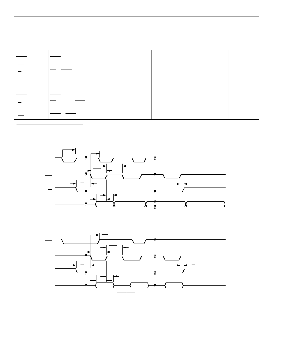
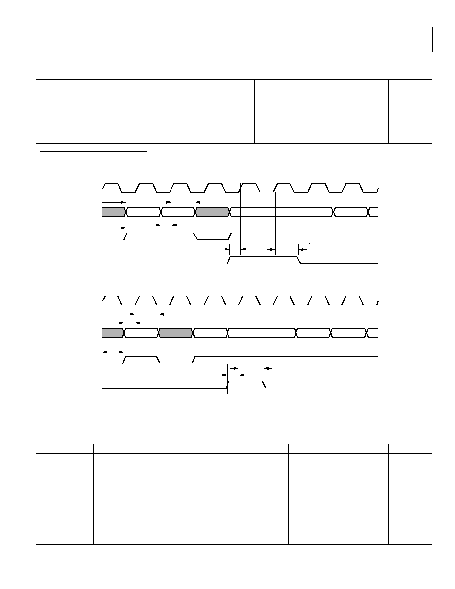
DREQ/DACK DMA MODE--SINGLE FIFO WRITE OPERATION
Table 6.
Parameter
Description
Min
Typ
Max
Unit
DREQ
PULSE
1
DREQ Pulse Width
1
15
JCLK cycles
2
t
DREQ
DACK Assert to Subsequent DREQ Delay
2.5
3.5 × JCLK + 7.5 ns
JCLK cycles
t
WESU
WE to DACK Setup
0
ns
t
SU
Data to DACK Deassert Setup
2
ns
t
HD
Data to DACK Deassert Hold
2
ns
DACK
LO
DACK Assert Pulse Width
2
JCLK
cycles
DACK
HI
DACK Deassert Pulse Width
2
JCLK
cycles
t
WEHD
WE Hold after DACK Deassert
0
ns
WFSRQ
WE Assert to FSRQ Deassert (FIFO Full)
1.5
2.5 × JCLK + 7.5 ns
JCLK cycles
t
DREQRTN
DACK to DREQ Deassert (DR × PULS = 0)
2.5
3.5 × JCLK + 7.5 ns
JCLK cycles
1
Applies to assigned DMA channel, if EDMOD0 or EDMOD1 <14:11> is programmed to a value that is not 0. Pulse width depends on the value programmed.
2
For a definition of JCLK, see the PLL section.
04723-013
WE
DACK
DREQ
HDATA
3
2
1
0
DREQ
PULSE
t
DREQ
DACK
HI
DACK
LO
t
WESU
t
SU
t
HD
t
WEHD
Figure 5. Single Write for DREQ/DACK DMA Mode for Assigned DMA Channel
(EDMOD0/EDMOD1 <14:11> NOT Programmed to a Value of 0000)
04723-014
WE
DACK
DREQ
HDATA
0
1
2
t
DREQRTN
DACK
HI
DACK
LO
t
WESU
t
SU
t
HD
t
WEHD
Figure 6. Single Write for DREQ/DACK DMA Mode for Assigned DMA Channel
(EDMOD0/EDMOD1 <14:11> Programmed to a Value of 0000)
ADV202
Rev. 0 | Page 9 of 40
04723-015
WEFB
DACK
DREQ
HDATA
0
1
2
DREQ
PULSE
t
DREQ
DACK
HI
DACK
LO
t
WESU
t
SU
t
HD
t
WEHD
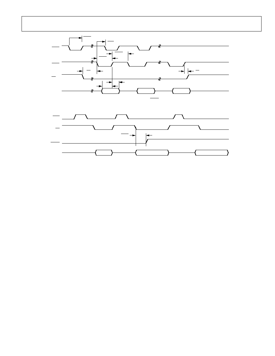
Figure 7. Fly-By DMA Mode --Single Write Cycle (DREQ Pulse Width Is Programmable)
04723-016
FSRQ0
WE
FSC0
HDATA
WFSRQ
FIFO NOT FULL
FIFO FULL
NOT WRITTEN TO FIFO
0
1
2
Figure 8. DCS DMA Mode--Single Write Access (Rev. 0.1 and Higher)

ADV202
Rev. 0 | Page 10 of 40
DREQ/DACK DMA MODE--SINGLE FIFO READ OPERATION
Table 7.
Parameter
Description
Min
Typ
Max
Unit
DREQ
PULSE
DREQ Pulse Width
1
1
15
JCLK cycles
2
t
DREQ
DACK Assert to Subsequent DREQ Delay
2.5
3.5 × JCLK + 7.5 ns
JCLK cycles
t
RDSU
RD to DACK Setup
0
ns
t
RD
DACK to Data Valid
2.5
11
ns
t
HD
Data Hold
1.5
ns
DACK
LO
DACK Assert Pulse Width
2
JCLK cycles
DACK
HI
DACK Deassert Pulse Width
2
JCLK
cycles
t
RDHD
RD Hold after DACK Deassert
0
ns
RDFSRQ
RD Assert to FSRQ Deassert (FIFO Empty)
1.5 2.5 × JCLK + 7.5 ns
JCLK cycles
t
DREQRTN
DACK to DREQ Deassert (DR × PULS = 0)
2.5 3.5 × JCLK + 7.5 ns
JCLK cycles
1
Applies to assigned DMA channel, if EDMOD0 or EDMOD1 <14:11> is programmed to a nonzero value.
2
For a definition of JCLK, see the
section.
PLL
04723-018
RD
DACK
DREQ
HDATA
0
1
2
t
RD
t
HD
DREQ
PULSE
t
DREQ
t
RDSU
t
RDHD
DACK
HI
DACK
LO
Figure 9. Single Read for DREQ/DACK DMA Mode for Assigned DMA Channel
(EDMOD0/EDMOD1 <14:11> NOT Programmed to a Value of 0000)
04723-019
RD
DACK
DREQ
HDATA
0
1
2
t
RD
t
HD
t
DREQRTN
t
RDSU
t
RDHD
DACK
HI
DACK
LO
Figure 10. Single Read forDREQ/DACK DMA Mode for Assigned DMA Channel
(EDMOD0/EDMOD1 <14:11> Programmed to a Value of 0000)

ADV202
Rev. 0 | Page 11 of 40
04723-020
RDFB
DACK
DREQ
HDATA
0
1
2
t
RD
t
HD
t
DREQ
DREQ
PULSE
t
RDSU
t
RDHD
DACK
HI
DACK
LO
Figure 11. Fly-By DMA Mode--Single Read Cycle
(DREQ Pulse Width Is Programmable)
04723-021
RD
FSRQ0
FCS0
HDATA
0
1
RDFSRQ
FIFO NOT EMPTY
FIFO EMPTY
Figure 12. DCS DMA Mode--Single Read Access (Rev. 0.1 and Higher)
ADV202
Rev. 0 | Page 12 of 40
EXTERNAL DMA MODE--FIFO WRITE, BURST MODE
Table 8.
Parameter
Desription
Min
Typ
Max
Unit
DREQ
PULSE
DREQ Pulse Width
1
1
15
JCLK cycles
2
t
DREQRTN
DACK to DREQ Deassert (DR × Pulse = 0)
2.5
3.5 × JCLK + 7.5 ns
JCLK cycles
t
DACKSU
DACK to WE Setup
0
ns
t
SU
Data Setup
2.5
ns
t
HD
Data Hold
2
ns
WE
LO
WE Assert Pulse Width
1.5
JCLK
cycles
WE
HI
WE Deassert Pulse Width
1.5
JCLK
cycles
t
DREQWAIT
DACK Deassert to Next DREQ
2.5
4.5 × JCLK + 7.5 ns
3
JCLK cycles
1
Applies to assigned DMA channel, if EDMOD0 or EDMOD1 <14:11> is programmed to a value that is NOT 0. Pulse width depends on the value programmed.
2
For a definition of JCLK, see the
section.
PLL
3
If sufficient space is available in FIFO.
04723-022
DREQ
DACK
WE
HDATA
WE
HI
WE
LO
t
DACKSU
t
HD
t
SU
0
1
13
14
15
t
DREQWAIT
DREQ
PULSE
Figure 13. Burst Write Cycle forDREQ/DMA Mode for Assigned DMA Channel
(EDMOD0/EDMOD1 <14:11> NOT Programmed to a Value of 0000)
04723-023
DREQ
DACK
WE
HDATA
WE
HI
WE
LO
t
DACKSU
t
HD
t
SU
0
1
13
14
15
t
DREQWAIT
t
DREQRTN
Figure 14. Burst Write Cycle for DREQ/DMA Mode for Assigned DMA Channel
(EDMOD0/EDMOD1 <14:11> Programmed to a Value of 0000)

ADV202
Rev. 0 | Page 13 of 40
04723-024
DREQ
DACK
WEFB
HDATA
WE
HI
WE
LO
t
DACKSU
t
HD
t
SU
0
1
13
14
15
t
DREQWAIT
t
DREQRTN
Figure 15. Burst Write Cycle for Fly-By DMA Mode
(DREQ Pulse Width Is Programmable)
EXTERNAL DMA MODE--FIFO READ, BURST MODE
Table 9.
Parameter
Description
Min
Typ
Max
Unit
DREQ
PULSE
DREQ Pulse Width
1
1
15
JCLK cycles
2
t
DREQRTN
DACK to DREQ Deassert (DR × PULS = 0)
2.5
3.5 × JCLK + 7.5 ns
JCLK cycles
t
DACK
SU
DACK to RD Setup
0
ns
t
RD
DACK to Data Valid
2.5
9.7
ns
t
HD
Data Hold
2.5
ns
RD
LO
RD Assert Pulse Width
1.5
JCLK
cycles
RD
HI
RD Deassert Pulse Width
1.5
JCLK
cycles
t
DREQWAIT
DACK Deassert to Next DREQ
2.5
3.5 × JCLK + 7.5 ns
3
JCLK cycles
1
Applies to assigned DMA channel, if EDMOD0 or EDMOD1 <14:11> is programmed to a value that is not 0. Pulse width depends on the value programmed.
2
For a definition of JCLK, see the
section.
PLL
3
If sufficient data is available in FIFO.
04723-025
DREQ
DACK
RD
HDATA
RD
HI
RD
LO
t
DACKSU
t
HD
0
1
13
14
15
t
DREQWAIT
DREQ
PULSE
t
RD
Figure 16. Burst Read Cycle for DREQ/DACK DMA Mode for Assigned DMA Channel
(EMOD0/EDMOD1 <14:11> NOT Programmed to a Value of 0
ADV202
Rev. 0 | Page 14 of 40
04723-026
DREQ
DACK
RD
HDATA
RD
HI
RD
LO
t
DACKSU
t
HD
0
1
13
14
15
t
DREQWAIT
t
DREQRTN
t
RD
Figure 17. Burst Read Cycle for DREQ/DACK DMA Mode for Assigned DMA Channel
( EMOD0/EDMOD1 <14:11> Programmed to a Value of 0000)
04723-027
DREQ
DACK
RDFB
HDATA
t
DACKSU
t
HD
0
1
13
14
15
t
DREQWAIT
t
DREQRTN
t
RD
Figure 18. Burst Read Cycle, Fly-By DMA Mode
(DREQ Pulse Width Is Programmable)
ADV202
Rev. 0 | Page 15 of 40
STREAMING MODE (JDATA)--FIFO READ/WRITE
Table 10.
Parameter
Description
Min
Typ
Max
Unit
JDATA
TD
MCLK to JDATA Valid
1.5
2.5 × JCLK + 7.0 ns
JCLK cycles
1
VALID
TD
MCLK to VALID Assert/ Deassert
1.5
2.5 × JCLK + .7.0 ns
JCLK cycles
HOLD
SU
HOLD Setup to Rising MCLK
3
ns
HOLD
HD
HOLD Hold from Rising MCLK
3
ns
JDATA
SU
JDATA Setup to Rising MCLK
3
ns
JDATA
HD
JDATA Hold from Rising MCLK
3
ns
1
For a definition of JCLK, see the
section.
PLL
04723-028
MCLK
JDATA
VALID
HOLD
HOLD
HD
HOLD
SU
VALID
TD
JDATA
SU
JDATA
TD
JDATA
HD
Figure 19. Streaming Mode Timing--Encode Mode JDATA Output
04723-029
MCLK
JDATA
VALID
HOLD
HOLD
HD
HOLD
SU
VALID
TD
JDATA
SU
JDATA
HD
Figure 20. Streaming Mode Timing--Decode Mode JDATA Input
VDATA MODE TIMING
Table 11.
Parameter
Description
Min
Typ
Max
Unit
VDATA
TD
VCLK to VDATA Valid Delay (VDATA Output)
12
ns
VDATA
SU
VDATA Setup to Rising VCLK (VDATA Input)
4
ns
VDATA
HD
VDATA Hold from Rising VCLK (VDATA Input)
4
ns
HSYNC
SU
HSYNC Setup to Rising VCLK
3
ns
HSYNC
HD
HSYNC Hold from Rising VCLK
4
ns
HSYNC
TD
VCLK to HSYNC Valid Delay
12
ns
VSYNC
SU
VSYNC Setup to Rising VCLK
3
ns
VSYNC
HD
VSYNC Hold from Rising VCLK
4
ns
VSYNC
TD
VCLK to VSYNC Valid Delay
12
ns
FIELD
SU
FIELD Setup to Rising VCLK
4
ns
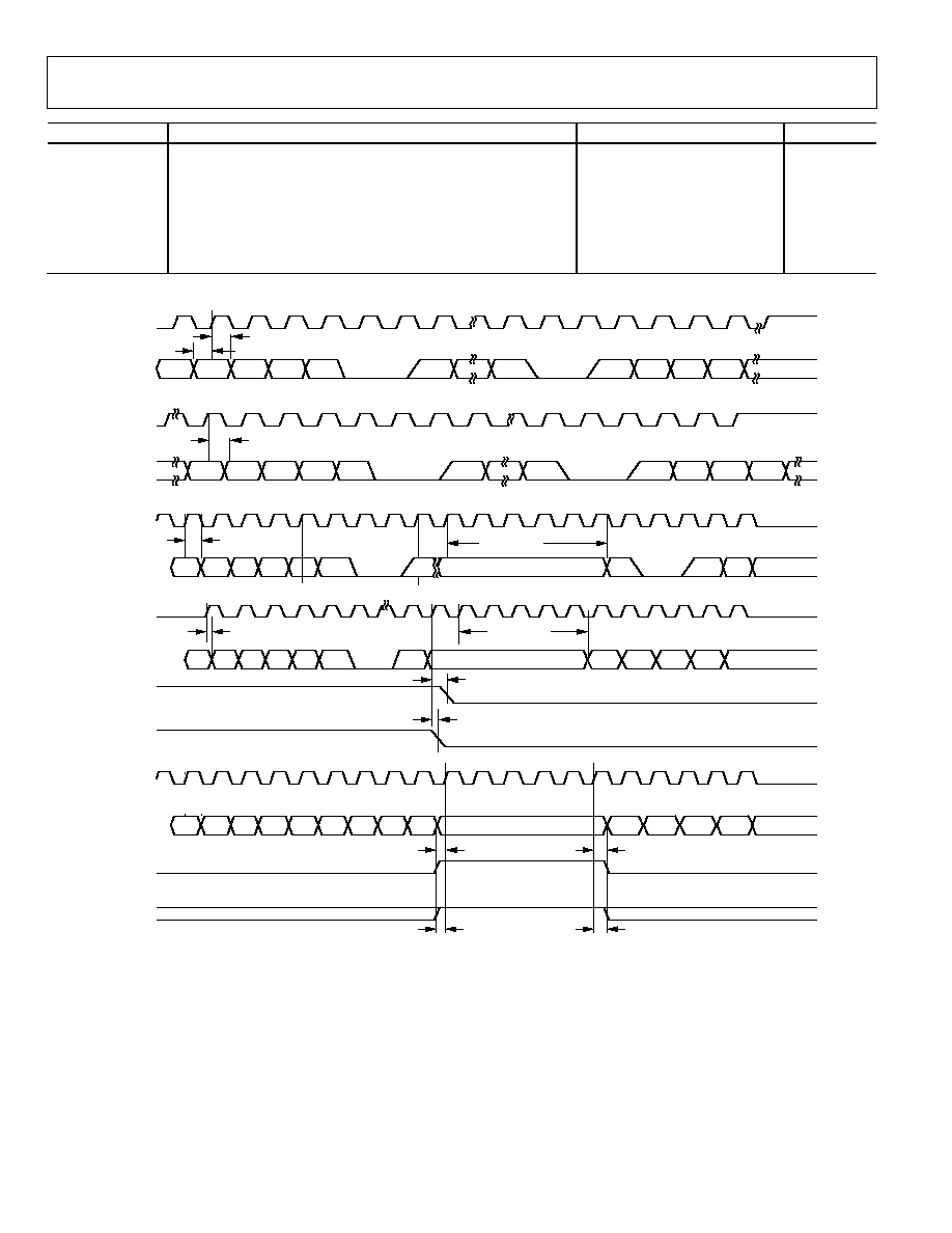
ADV202
Rev. 0 | Page 16 of 40
Parameter
Description
Min
Typ
Max
Unit
FIELD
HD
FIELD Hold from Rising VCLK
3
ns
FIELD
TD
VCLK to FIELD Valid
12
SYNC DELAY
Decode Data Sync Delay for HD Input with EAV/SAV Codes
7
VCLK cycles
Decode Data Sync Delay for SD Input with EAV/SAV Codes
9
VCLK cycles
Decode Data Sync Delay for DUAL_LANE (Extended) Input
7
VCLK cycles
Decode Data Sync Delay for HVF Input (from First Rising VCLK after
HSYNC Low to First Data Sample)
10
VCLK
cycles
04723-030
Cr
Y
Cb
Y
FF
EAV
FF
SAV
Cb
Y
Cr
VDATA
HD
VDATA
SU
VCLK
VDATA(IN)
ENCODE CCIR-656 LINE
VDATA
TD
VCLK
VDATA(OUT)
VDATA(OUT)
Cr
Y
Cb
Y
FF
EAV
FF
SAV
Cb
Y
Cr
DECODE MASTER CCIR-656 LINE
VCLK
VDATA(OUT)
VDATA
TD
SYNC DELAY
Cr
Y
Y
Cb
Y
FF
EAV
FF
SAV
Cb
Y
*HSYNC AND VSYNC DO NOT HAVE TO BE APPLIED SIMULTANEOUSLY
VCLK
VDATA(IN)
HSYNC
VSYNC
Cr
Y
Y
Cb
Y
Cr
Y
Cb
Y
Y
Cr
Y
Cb
Cb
HSYNC
SU
ENCODE HVF MODE
DECODE SLAVE CCIR-656 LINE
HSYNC
HD
VSYNC
SU
VSYNC
HD
Cb
Y
Cr
Y
Cb
Cb
Y
VCLK
HSYNC
VSYNC
DECODE SLAVE HVF MODE
HSYNC
HD
*
VDATA
TD
SYNC DELAY
VSYNC
HD
*
Cb
Y
Cr
Y
Figure 21. Video Mode Timing
ADV202
Rev. 0 | Page 17 of 40
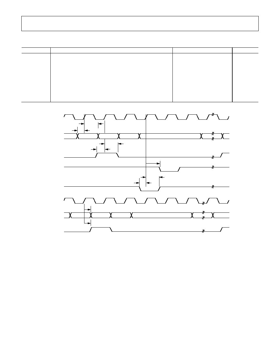
RAW PIXEL MODE TIMING
Table 12.
Parameter
Description
Min
Typ
Max
Unit
VDATA
TD
VCLK to PIXELDATA Valid Delay (PIXELDATA Output)
12
ns
VDATA
SU
PIXELDATA Setup to Rising VCLK (PIXELDATA Input)
4
ns
VDATA
HD
PIXELDATA Hold from Rising VCLK (PIXELDATA Input)
4
ns
VRDY
TD
VCLK to VRDY Valid Delay
12
ns
VFRM
SU
VFRM Setup to Rising VCLK (VFRAME Input)
3
ns
VFRM
HD
VFRM Hold from Rising VCLK (VFRAME Input)
4
ns
VFRM
TD
VCLK to VFRM Valid Delay (VFRAME Output)
12
ns
VSTRB
SU
VSTRB Setup to Rising VCLK
4
ns
VSTRB
HD
VSTRB Hold from Rising VCLK
3
ns
N
N
0
1
2
04723-031
VCLK
VCLK
PIXEL
DATA(IN)
PIXEL
DATA
VFRM(OUT)
VFRM(IN)
VRDY
VSTRB
N1
N
0
1
2
VRFM
TD
VDATA
TD
VSTRB
SU
VSTRB
HD
VFRM
SU
VFRM
HD
VDATA
HD
VDATA
SU
VRDY
TD
Figure 22. Raw Pixel Mode Timing
ADV202
Rev. 0 | Page 18 of 40
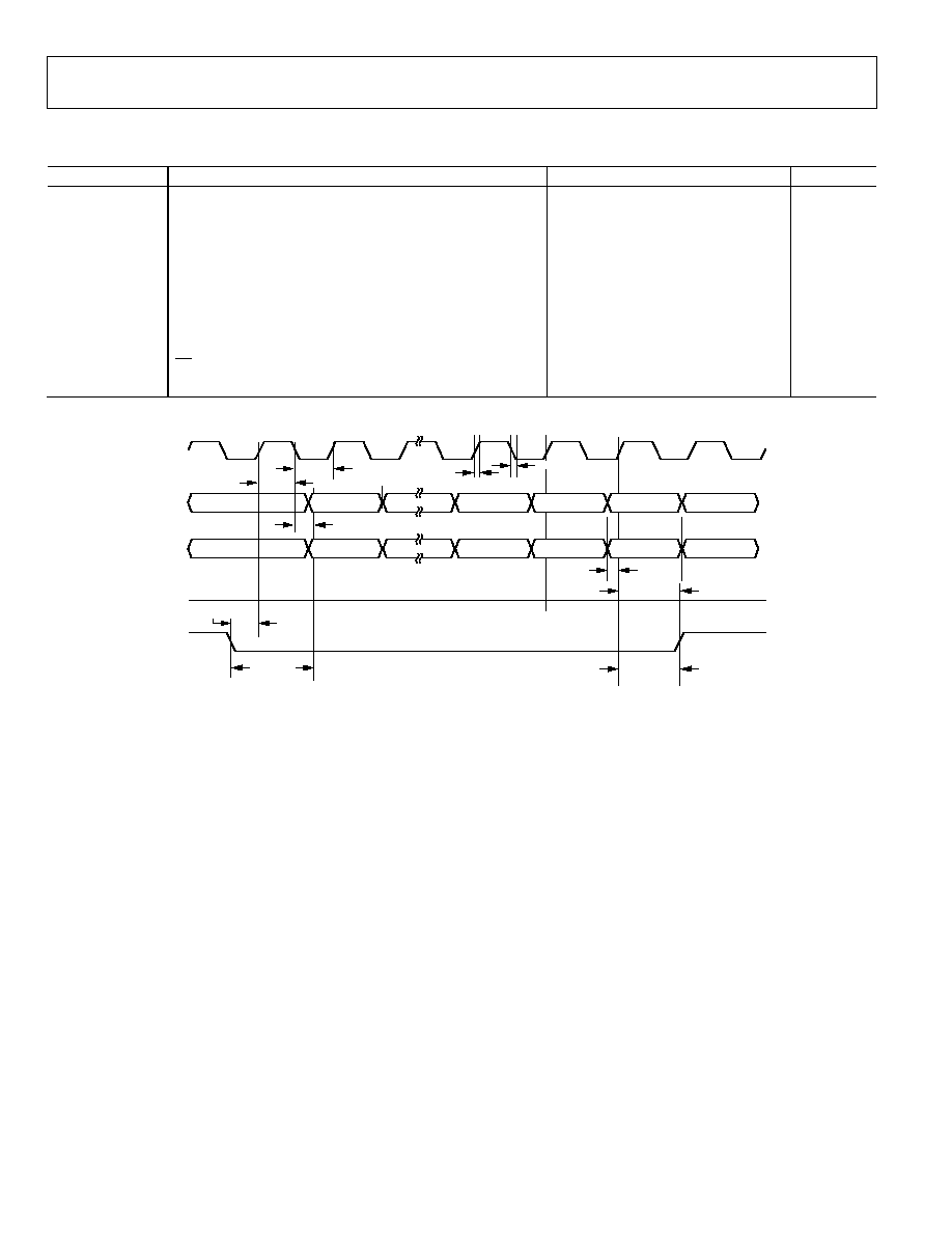
SPI PORT TIMING
Table 13.
Parameter
Description
Min
Typ
Max
Unit
SCLK
FALL
S_CLK Fall Time
5
ns
SCLK
RIS
S_CLK Rise Time
5
ns
SCLK_hi
SCLK high time
75
ns
SCLK_lo
SCLK Low Time
75
ns
Data_su
Data Setup Time
6.5
ns
Data_hd
Data Hold Time
6.5
ns
CSEL_
SU
Active Setup Time
135
ns
CSEL_
HD
Active Hold Time
155
ns
DV_SCLK
SCLK to Output Data Valid
2
ns
DV_CS
CS to Output Data Valid
36
ns
SCLK
SCLK Period
150
ns
04723-032
S_CLK
S_MO
S_MI
S_CSEL
CSEL
SU
MSB
LSB
MSB
LSB
SCLK_HI
SCLK_LO
DV_SCLK
SCLK
RISE
SCLK
FALL
DATA
SU
DATA
HD
CSEL
HD
DC_CS
Figure 23. SPI Port--Input Timing
ADV202
Rev. 0 | Page 19 of 40
PIN BGA ASSIGNMENTS AND FUNCTION DESCRIPTIONS
PIN BGA ASSIGNMENTS
Table 14. Pin BGA Assignments for 121-Lead Package
Pin No.
Pin Location
Pin Description
1
A1
DGND
2
A2
HDATA[2]
3
A3
VDD
4
A4
DGND
5
A5
HDATA[0]
6
A6
HDATA[1]
7
A7
VDATA[1]
8
A8
VDD
9
A9
DGND
10
A10
VDATA[0]
11
A11
DGND
12
B1
HDATA[3]
13
B2
HDATA[4]
14
B3
HDATA[5]
15
B4
HDATA[7]
16
B5
HDATA[8]
17
B6
IOVDD
18
B7
VDATA[6]
19
B8
VDATA[5]
20
B9
VDATA[4]
21
B10
VDATA[2]
22
B11
VDATA[3]
23
C1
DGND
24
C2
HDATA[6]
25
C3
HDATA[9]
26
C4
HDATA[10]
27
C5
HDATA[11]
28
C6
IOVDD
29
C7
VDATA[9]
30
C8
IOVDD
31
C9
VDATA[8]
32
C10
VDATA[7]
33
C11
DGND
34
D1
HDATA[12]
35
D2
HDATA[13]
36
D3
HDATA[14]
37
D4
HDATA[15]
38
D5
IOVDD
39
D6
DGND
40
D7
VDD
41
D8
VSYNC
42
D9
HSYNC
43
D10
VDATA[10]
44
D11
VDATA[11]
45
E1
DGND
46
E2
HDATA[18]_VDATA[14]
47
E3
HDATA[17]_VDATA[13]
48
E4
HDATA[16]_VDATA[12]
49
E5
DGND
Pin No.
Pin Location
Pin Description
50
E6
DGND
51
E7
DGND
52
E8
IOVDD
53
E9
VCLK
54
E10
FIELD
55
E11
DGND
56
F1
DGND
57
F2
HDATA[19]_VDATA[15]
58
F3
HDATA[20]_VDATA[16]
59
F4
HDATA[21]_VDATA[17]
60
F5
DGND
61
F6
DGND
62
F7
DGND
63
F8
DREQ0
64
F9
DACK0
65
F10
DREQ1
66
F11
DGND
67
G1
DGND
68
G2
HDATA[22]_VDATA[18]
69
G3
HDATA[23]_VDATA[19]
70
G4
HDATA[24]_VDATA[20]_JDATA[0]
71
G5
DGND
72
G6
DGND
73
G7
DGND
74
G8
IOVDD
75
G9
DACK1
76
G10
IRQ
77
G11
DGND
78
H1
HDATA[28]_JDATA[4]
79
H2
HDATA[27]_VDATA[23]_JDATA[3]
80
H3
HDATA[26]_VDATA[22]_JDATA[2]
81
H4
HDATA[25]_VDATA[21]_JDATA[1]
82
H5
IOVDD
83
H6
DGND
84
H7
VDD
85
H8
ACK
86
H9
RD
87
H10
ADDR[1]
88
H11
ADDR[3]
89
J1
DGND
90
J2
HDATA[31]_JDATA[7]
91
J3
HDATA[30]_JDATA[6]
92
J4
HDATA[29]_JDATA[5]
93
J5
IOVDD
94
J6
TEST1
95
J7
WE
96
J8
CS
97
J9
ADDR[0]

ADV202
Rev. 0 | Page 20 of 40
Pin No.
Pin Location
Pin Description
98
J10
TEST3
99
J11
DGND
100
K1
SCOMM[4]
101
K2
SCOMM[3]
102
K3
SCOMM[0]
103
K4
SCOMM[1]
104
K5
IOVDD
105
K6
IOVDD
106
K7
IOVDD
107
K8
ADDR[2]
108
K9
TEST2
109
K10
TEST5
Pin No.
Pin Location
Pin Description
110
K11
DGND
111
L1
DGND
112
L2
SCOMM[7]
113
L3
SCOMM[6]
114
L4
SCOMM[5]
115
L5
SCOMM[2]
116
L6
TEST4
117
L7
RESET
118
L8
DGND
119
L9
MCLK
120
L10
PLLVDD
121
L11
DGND
Table 15. Pin BGA Assignments for 144-Lead Package
Pin No.
Pin Location
Pin Description
1
A1
DGND
2
A2
HDATA[2]
3
A3
HDATA[1]
4
A4
HDATA[0]
5
A5
DGND
6
A6
DGND
7
A7
DGND
8
A8
DGND
9
A9
VDATA[2]
10
A10
VDATA[1]
11
A11
VDATA[0]
12
A12
DGND
13
B1
HDATA[5]
14
B2
HDATA[4]
15
B3
HDATA[3]
16
B4
IOVDD
17
B5
DGND
18
B6
VDD
19
B7
VDD
20
B8
DGND
21
B9
IOVDD
22
B10
VDATA[5]
23
B11
VDATA[4]
24
B12
VDATA[3]
25
C1
HDATA[8]
26
C2
HDATA[7]
27
C3
HDATA[6]
28
C4
IOVDD
29
C5
DGND
30
C6
VDD
31
C7
VDD
32
C8
DGND
33
C9
IOVDD
34
C10
VDATA[8]
35
C11
VDATA[7]
36
C12
VDATA[6]
37
D1
HDATA[11]
Pin No.
Pin Location
Pin Description
38
D2
HDATA[10]
39
D3
HDATA[9]
40
D4
IOVDD
41
D5
DGND
42
D6
VDD
43
D7
VDD
44
D8
DGND
45
D9
IOVDD
46
D10
VDATA[11]
47
D11
VDATA[10]
48
D12
VDATA[9]
49
E1
HDATA[14]
50
E2
HDATA[13]
51
E3
HDATA[12]
52
E4
DGND
53
E5
DGND
54
E6
DGND
55
E7
DGND
56
E8
DGND
57
E9
FIELD
58
E10
VSYNC
59
E11
HSYNC
60
E12
VCLK
61
F1
HDATA[18]_VDATA[14]
62
F2
HDATA[17]_VDATA[13]
63
F3
HDATA[16]_VDATA[12]
64
F4
HDATA[15]
65
F5
DGND
66
F6
DGND
67
F7
DGND
68
F8
DGND
69
F9
DACK1
70
F10
DREQ1
71
F11
DACK0
72
F12
DREQ0
73
G1
HDATA[22]_VDATA[18]

ADV202
Rev. 0 | Page 21 of 40
Pin No.
Pin Location
Pin Description
74
G2
HDATA[21]_VDATA[17]
75
G3
HDATA[20]_VDATA[16]
76
G4
HDATA[19]_VDATA[15]
77
G5
DGND
78
G6
DGND
79
G7
DGND
80
G8
DGND
81
G9
DGND
82
G10
IRQ
83
G11
ACK
84
G12
RD
85
H1
HDATA[26]_VDATA[22]_JDATA[2]
86
H2
HDATA[25]_VDATA[21]_JDATA[1]
87
H3
HDATA[24]_VDATA[20]_JDATA[0]
88
H4
HDATA[23]_VDATA[19]
89
H5
DGND
90
H6
DGND
91
H7
DGND
92
H8
DGND
93
H9
DGND
94
H10
WR
95
H11
CS
96
H12
ADDR[0]
97
J1
HDATA[30]_JDATA[6]
98
J2
HDATA[29]_JDATA[5]
99
J3
HDATA[28]_JDATA[4]
100
J4
HDATA[27]_VDATA[23]_JDATA[3]
101
J5
DGND
102
J6
VDD
103
J7
VDD
104
J8
DGND
105
J9
DGND
106
J10
ADDR[1]
107
J11
ADDR[2]
108
J12
ADDR[3]
109
K1
SCOMM[1]
Pin No.
Pin Location
Pin Description
110
K2
SCOMM[0]
111
K3
HDATA[31]_JDATA[7]
112
K4
IOVDD
113
K5
DGND
114
K6
VDD
115
K7
VDD
116
K8
DGND
117
K9
IOVDD
118
K10
TEST3
119
K11
TEST2
120
K12
TEST1
121
L1
SCOMM[4]
122
L2
SCOMM[3]
123
L3
SCOMM[2]
124
L4
IOVDD
125
L5
DGND
126
L6
VDD
127
L7
VDD
128
L8
DGND
129
L9
IOVDD
130
L10
TEST5
131
L11
RESET
132
L12
MCLK
133
M1
DGND
134
M2
SCOMM[7]
135
M3
SCOMM[6]
136
M4
SCOMM[5]
137
M5
DGND
138
M6
DGND
139
M7
DGND
140
M8
DGND
141
M9
TEST4
142
M10
PLLVDD
143
M11
DGND
144
M12
DGND
ADV202
Rev. 0 | Page 22 of 40
PIN FUNCTION DESCRIPTIONS
Table 16.
Mnemonic
Pins
Used
121-Pin
Package
144-Pin
Package
I/O
Description
MCLK 1
L9
L12 I
System Input Clock. For details, see the PLL section. Maximum input
frequency on MCLK is 74.25 MHz.
RESET
1 L7
L11
I Reset. Causes the ADV202 to immediately reset. CS, RD, WE, DACK0,
DACK1, DREQ0, and DREQ1 must be held high when a RESET is
applied.
HDATA<15:0>
16
D4D1, C5
C3, B5, B4, C2,
B3B1, A2,
A6A5
F4, E1E3,
D1D3, C1
C3, B1B3, A2,
A3, A4
I/O
Host Data Bus. With HDATA<23:16>, <27:24>, <31:28>, these pins
make up the 32-bit wide host data bus. The async host interface is
interfaced together with ADDR<3:0>, CS, WE, RD, and ACK.
Unused HDATA pins should be pulled down via a 10 k resistor.
ADDR<3:0>
4
H11, K8, H10,
J9
J12, J11, J10,
H12
I
Address Bus for the Host Interface.
CS
1 J8
H11
I Chip Select.This signal is used to qualify addressed read and write
access to the ADV202 using the host interface.
WE
1
J7
H10
I
Write Enable Used with the Host Interface.
RDFB
Read Enable when Fly-By DMA Is Enabled.
Note: Simultaneous assertion of WE and DACK low activates the
HDATA bus, even if the DMA channels are disabled.
RD
1
H9
G12
I
Read Enable Used with the Host Interface.
WEFB
Write Enable when Fly-By DMA Is Enabled.
Note: Simultaneous assertion of RD and DACK low activates the
HDATA bus, even if the DMA channels are disabled.
ACK
1
H8
G11
O
Acknowledge. Used for direct register accesses. This signal indicates
that the last register access was successful.
Note: Due to synchronization issues, control and status register
accesses might incur an additional delay, so the host software should
wait for acknowledgment from the ADV202.
Accesses to the FIFOs (external DMA modes), on the other hand, are
guaranteed to occur immediately, provided that space is available,
and should not wait for ACK, provided that the timing constraints
are observed.
If ACK is shared with more than one device, ACK should be connected
to a pull-up resistor (10 k) and the PLL_HI register, Bit 4, must be set
to 1.
IRQ
1
G10
G10
O
Interrupt. This pin indicates that the ADV202 requires the attention of
the host processor. This pin can be programmed to indicate the status
of the internal interrupt conditions within the ADV202. The interrupt
sources are enabled via bits in register EIRQIE.
DREQ0
1 F8
F12
O Data Request for external DMA Interface. Indicates that the ADV202
is ready to send/receive data to/from the FIFO assigned to DMA
Channel 0.
FSRQ0
O
Used in DCS-DMA Mode. Service request from the FIFO assigned to
Channel 0 (asynchronous mode).
VALID
O
Valid Indication for JDATA Input/Output Stream. Polarity of this pin is
programmable in the EDMOD0 register. VALID is always an output.
CFG<1>
I
Boot Mode Configuration. This pin is read on reset to determine the
boot configuration of the on-board processor. The pin should be tied
to IOVDD or DGND through a 10 k resistor.
DACK0
1
F9
F11
I
Data Acknowledge for External DMA Interface. Signal from the host
CPU, which indicates that the data transfer request (DREQ0) has been
acknowledged and data transfer can proceed. This pin must be held
high at all times, if the DMA interface is not used, even if the DMA
channels are disabled.

ADV202
Rev. 0 | Page 23 of 40
Mnemonic
Pins
Used
121-Pin
Package
144-Pin
Package
I/O
Description
HOLD
I
External Hold Indication for JDATA Input/Output Stream. Polarity is
programmable in the EDMOD0 register. This pin is always an input.
FCS0
I
Used in DCS-DMA Mode. Chip select for the FIFO assigned to
Channel 0 (asynchronous mode).
DREQ1
1
F10
F10
O
Data Request for External DMA Interface. Indicates that the ADV202
is ready to send/receive data to/from the FIFO assigned to DMA
Channel 1.
FSRQ1
O
Used in DCS-DMA Mode. Service request from the FIFO assigned to
Channel 1 (asynchronous mode).
CFG<2>
I
Boot Mode Configuration. This pin is read on reset to determine the
boot configuration of the on-board processor. The pin should be tied
to IOVDD or DGND through a 10 k resistor.
DACK1
1
G9
F9
I
Data Acknowledge for External DMA Interface. Signal from the host
CPU, which indicates that the data transfer request (DREQ1) has been
acknowledged and data transfer can proceed. This pin must be held
high at all times unless a DMA or JDATA access is occurring. This pin
must be held high at all times, if the DMA interface is not used, even if
the DMA channels are disabled.
FCS1
I
Used in DCS-DMA Mode. Chip select for the FIFO assigned to
Channel 1 (asynchronous mode).
HDATA<31:28> 4
J2J4, H1
K3, J1J3
I/O
Host Expansion Bus.
JDATA<7:4>
I/O
JDATA Bus (JDATA Mode).
HDATA<27:24> 4
H2H4, G4
J4, H1H3
I/O
Host Expansion Bus.
JDATA<3:0>
I/O
JDATA Bus (JDATA Mode).
VDATA<23:20>
I/O
Video Data Expansion Bus.
HDATA<23:16> 8
G3, G2, F4, F3,
F2 E2, E3, E4
H4, G1G4,
F1F3
I/O
Host Expansion Bus.
VDATA<19:12>
I/O
Video Data Expansion Bus. Extended pixel interface mode. Used for
video formats that use Y and CrCb on separate buses.
SCOMM<7>
8
L2
M2
I/O
When not used, this pin should be tied low.
SCOMM<6>
L3
M3
I/O
When not used, this pin should be tied low.
SCOMM<5>
L4
M4
I/O
This pin must be used in multiple chip mode to align the outputs of
two or more ADV202s. For details, see the Applications section and
the ADV202 Multichip Application application note. When not used,
this pin should be tied low.
SCOMM<4>
K1
L1
O
LCODE Output in Encode Mode. When LCODE is enabled, the output
on this pin indicates on a high transition that the last data-word for a
field has been read from the FIFO. For an 8-bit interface, such as
JDATA, LCODE is asserted for four consecutive bytes and is enabled
by default.
SCOMM<3>
K2
L2
O
SPI interface: S_CSEL. When not used, this pin should be tied low.
Used only with boot mode 6.
SCOMM<2>
L5
L3
O
SPI interface: S_MO. When not used, this pin should be tied low.
Used only with boot mode 6.
SCOMM<1>
K4
K1
I
SPI interface: S_MI. When not used, this pin should be tied low.
Used only with boot mode 6.
SCOMM<0>
K3
K2
O
SPI interface: S_CLK. When not used, this pin should be tied low.
Used only with boot mode 6.
VCLK
1
E9
E12
I
Video Data Clock. Must be supplied, if video data is input/output on
the VDATA bus.
VDATA<11:0>
12
D11, D10, C7,
C9, C10, B7,
B8, B9, B11,
B10, A7, A10
D10D12,
C10C12,
B10B12,
A9A11
I/O
Video Data. Unused pins should be pulled down via a 10 k resistor.

ADV202
Rev. 0 | Page 24 of 40
Mnemonic
Pins
Used
121-Pin
Package
144-Pin
Package
I/O
Description
VSYNC
1
D8
E10
I/O
Vertical Sync for Video Mode.
VFRM
Raw Pixel Mode Framing Signal. Indicates first sample of a tile when
asserted high.
HSYNC
1
D9
E11
I/O
Horizontal Sync for Video Mode.
VRDY
O
Raw Pixel Mode Ready Signal.
FIELD
1
E10
E9
I/O
Field Sync for Video Mode.
VSTRB
I
Raw Pixel Mode Transfer Strobe.
TEST1
1
J6
K12
I
This pin should be connected to ground via a pull-down resistor.
TEST2
1
K9
K11
I
This pin should be connected to ground via a pull-down resistor.
TEST3
1
J10
K10
I
This pin should be connected to ground via a pull-down resistor.
TEST4
1
L6
M9
I
This pin should be connected to ground via a pull-down resistor.
TEST5
1
K10
L10
O
No connect.
VDD
A3, A8, D7, H7
B6, B7, C6, C7,
D6, D7, J6, J7,
K6, K7, L6, L7
V
Positive Supply for Core.
DGND
A1, A11, A4,
A9, C1, C11,
D6, E1, E5E7,
E11, F1, F5
F7, F11, G1,
G5G7, G11,
H6, J1, J11,
K11, L1, L8,
L11
A1, A5A8,
A12, B5, B8,
C5, C8, D5, D8,
E4E8, F5F8,
G5G9, H5
H9, J5, J8J9,
K5, K8, L5, L8,
M1, M5M8,
M11, M12
GND Ground.
PLLVDD
1
L10
M10
V
Positive Supply for PLL.
IOVDD
B6, C6, C8, D5,
E8, G8, H5, J5,
K5, K6, K7
B4, B9, C4, C9,
D4, D9, K4, K9,
L4, L9
V
Positive Supply for I/O.

ADV202
Rev. 0 | Page 25 of 40
THEORY OF OPERATION
The input video or pixel data is passed on to the ADV202's pixel
interface, where samples are de-interleaved and passed on to the
wavelet engine, where each tile or frame is decomposed into
subbands using the 5/3 or 9/7 filters. The resultant wavelet
coefficients are then written to internal memory. The entropy
codecs then code the image data so that it conforms to the
JPEG2000 standard. An internal DMA provides high bandwidth
memory-to-memory transfers, as well as high performance
transfers between functional blocks and memory.
WAVELET ENGINE
The ADV202 provides a dedicated wavelet transform processor
based on the Analog Devices proven and patented SURFTM
technology. This processor can perform up to six wavelet
decomposition levels on a tile. In encode mode, the wavelet
transform processor takes in uncompressed samples, performs
the wavelet transform and quantization, and writes the wavelet
coefficients in all frequency subbands to internal memory. Each
of these subbands is then further broken down into code blocks.
The code-block dimensions can be user-defined, and are used
by the wavelet transform processor to organize the wavelet
coefficients into code blocks when writing to internal memory.
Each completed code block is then entropy coded by one of the
entropy codecs.
In decode mode, wavelet coefficients are read from internal
memory and recomposed into uncompressed samples.
ENTROPY CODECS
The entropy codec block performs context modeling and
arithmetic coding on a code block of the wavelet coefficients.
Additionally, this block also performs the distortion metric
calculations during compression that are required for optimal
rate and distortion performance. Because the entropy coding
process is the most computationally intensive operation in the
JPEG2000 compression process, three dedicated hardware
entropy codecs are provided on the ADV202.
EMBEDDED PROCESSOR SYSTEM
The ADV202 incorporates an embedded 32-bit RISC processor.
This processor is used for configuration, control, and manage-
ment of the dedicated hardware functions, as well as for parsing
and generation of the JPEG2000 code stream. The processor
system includes ROM and RAM for both program and data
memory, an interrupt controller, standard bus interfaces, and
other hardware functions such as timers and counters.
MEMORY SYSTEM
The memory system's main function is to manage wavelet
coefficient data, interim code-block attribute data, and
temporary work space for creating, parsing, and storing the
JPEG2000 code stream. The memory system can also be used
for program and data memory for the embedded processor.
INTERNAL DMA ENGINE
The internal DMA engine provides high bandwidth memory-
to-memory transfers, as well as high performance transfers
between memory and functional blocks. This function is critical
for high speed generation and parsing of the code stream.

ADV202
Rev. 0 | Page 26 of 40
ADV202 INTERFACE
There are several possible modes to interface to the ADV202
using the VDATA bus and the HDATA bus or the HDATA bus
alone.
VIDEO INTERFACE (VDATA BUS)
The video interface can be used in applications in which
uncompressed pixel data is on a separate bus from compressed
data. For example, it is possible to use the VDATA bus to input
uncompressed video while using the HDATA bus to output the
compressed data. This interface is ideal for applications
requiring very high throughput such as live video capture.
Optionally, the ADV202 interlaces ITU.R-BT656 resolution
video on the fly prior to wavelet processing, which yields
significantly better compression performance for temporally
coherent frame-based video sources. Additionally, high
definition digital video such as SMPTE274M (1080i) is
supported using two or more ADV202 devices.
The video interface can support video data or still image data
input/output, 8-, 10-, and 12-bit single or multiplexed
components, and dual-lane 8-, 10-, and 12-bit components. The
VDATA interface supports digital video in YCbCr format in
single input mode or Y and CbCr in dual-lane input mode.
YCbCr data must be in 4:2:2 format.
Video data can be input/output in several different modes on
the VDATA bus, as described in Table 17. In all these modes, the
pixel clock must be input on the VCLK pin.
Table 17. Video Input/Output Modes
Mode Description
EAV/SAV
Accepts video with embedded EAV/SAV codes,
where the YCbCr data is interleaved onto a single
bus.
HVF
Accepts video data accompanied with separate H,
V, and F signals where YCbCr data is interleaved
onto a single bus.
Extended
Y and CrCb are on separate buses accompanied by
EAV/SAV codes.
Raw video Used for still picture data and nonstandard video.
VFRM, VSTRB, and VRDY are used to program the
dimensions of the image.
HDTV
For applications in which video data is clocked into
the part at higher rates than 27 MHz.
HOST INTERFACE (HDATA BUS)
The ADV202 can connect directly to a wide variety of host
processors and ASICs using an asynchronous SRAM-style
interface, DMA accesses or streaming mode (JDATA) interface.
The ADV202 supports 16- and 32-bit buses for control and 8-,
16-, and 32-bit buses for data transfer.
The control and data channel bus widths can be specified
independently, which allows the ADV202 to support
applications that require control and data buses of different
widths.
The host interface is used for configuration, control, and status
functions, as well as for transferring compressed data streams. It
can be used for uncompressed data transfers in certain modes.
The host interface can be shared by as many as four concurrent
data streams in addition to control and status communications.
The data streams are
·
Uncompressed tile data (for example, still image data)
·
Fully encoded JPEG2000 code stream (or unpackaged code
blocks)
·
Code-block attributes
·
Ancillary data
The ADV202 uses big endian byte alignment for 16- and 32-bit
transfers. All data is left-justified (MSB).
Pixel Input on the Host Interface
Pixel input on the host interface supports 8-, 10-, 12-, 14-, and
16-bit raw pixel data formats. It can be used for pixel (still
image) input/output or compressed video output. Because there
are no timing codes or sync signals associated with the input
data on the host interface, dimension registers and internal
counters are used and must be programmed to indicate the start
and end of the frame. See the ADV202 in HIPI Mode technical
note for details on how to use the ADV202 in this mode.
Host Bus Configuration
For maximum flexibility, the host interface provides several
configurations to meet particular system requirements. The
default bus mode uses the same pins to transfer control, status,
and data to and from the ADV202. In this mode, the ADV202
can support 16- and 32-bit control transfers and 8-, 16-, and
32-bit data transfers. The size of these busses can be selected
independently, allowing, for example, a 16-bit microcontroller
to configure and control the ADV202 while still providing
32-bit data transfers to an ASIC or external memory system.
DIRECT AND INDIRECT REGISTERS
To minimize pin count and cost, the number of address pins has
been limited to four, which yields a total direct address space of
16 locations. These locations are most commonly used by the
external controller and are, therefore, accessible directly. All
other registers in the ADV202 can be accessed indirectly
through the IADDR and IDATA registers.

ADV202
Rev. 0 | Page 27 of 40
CONTROL ACCESS REGISTERS
With the exception of the indirect address and data registers
(IADDR and IDATA), all control/status registers in the ADV202
are 16 bits wide and are half-word (16-bit) addressable only.
When 32-bit host mode is enabled, the upper 16 bits of the
HDATA bus are ignored on writes and return all zeros on reads
of 16-bit registers.
PIN CONFIGURATION AND BUS SIZES/MODES
The ADV202 provides a wide variety of control and data
configurations, which allows it to be used in many applications
with little or no glue logic. The following modes are configured
using the BUSMODE register. In the following descriptions, host
refers to normal addressed accesses (CS/RD/WR/ADDR) and
data refers to external DMA accesses (DREQ/DACK).
32-Bit Host/32-Bit Data
In this mode, the HDATA<31:0> pins provide full 32-bit wide
data access to PIXEL, CODE, ATTR, and ANCL FIFOs. The
expanded video interface (VDATA) is not available in this
mode.
16-Bit Host/32-Bit Data
This mode allows a 16-bit host to configure and communicate
with the ADV202 while still allowing 32-bit accesses to the
PIXEL, CODE, ATTR, and ANCL FIFOs using the external
DMA capability.
All addressed host accesses are 16 bits and, therefore, use only
the HDATA<15:0> pins. The HDATA<31:16> pins provide the
additional 16 bits necessary to support the 32-bit external DMA
transfers to and from the FIFOs only. The expanded video
interface (VDATA) is not available in this mode.
16-Bit Host/16-Bit Data
This mode uses 16-bit transfers, if used for host or external
DMA data transfers. This mode allows for the use of the
extended pixel interface modes.
16-Bit Host/8-Bit Data (JDATA Bus Mode)
This mode provides separate data input/output and host control
interface pins. Host control accesses are 16 bits and use
HDATA<15:0>, while the dedicated data bus uses JDATA<7:0>.
JDATA uses a valid/hold synchronous transfer protocol. The
direction of the JDATA bus is determined by the mode of the
ADV202. If the ADV202 is encoding (compression), then
JDATA<7:0> is an output. If the ADV202 is decoding
(decompression), then JDATA<7:0> is an input. Host control
accesses remain asynchronous. See also JDATA section below.
STAGE REGISTER
Because the ADV202 contains both 16-bit and 32-bit registers
and its internal memory is mapped as 32-bit data, a mechanism
has been provided to allow 16-bit hosts to access these registers
and memory locations using the stage register (STAGE). STAGE
is accessed as a 16-bit register using HDATA[15:0]. Prior to
writing to the desired register, the stage register must be written
with the upper (most significant) half-word.
When the host subsequently writes the lower half-word to the
desired control register, HDATA is combined with the
previously staged value to create the required 32-bit value that is
written. When a register is read, the upper (most significant)
half-word is returned immediately on HDATA and the lower
half-word can be retrieved by reading the stage register on a
subsequent access. For details on using the stage register, see the
ADV202 User's Guide.
Note: The stage register does not apply to the four data channels
(PIXEL, CODE, ATTR, or ANCL). These channels are always
accessed at the specified data width and do not require the use
of the stage register.
JDATA MODE
JDATA mode is typically used only when the dedicated video
interface (VDATA) is also enabled. This mode allows code
stream data (compressed data compliant with JPEG2000) to be
input or output on a single dedicated 8-bit bus (JDATA<7:0>).
The bus is always an output during compression operations, and
is an input during decompression.
A 2-pin handshake is used to transfer data over this
synchronous interface. VALID is used to indicate that the
ADV202 is ready to provide or accept data and is always an
output. HOLD is always an input and is asserted by the host if it
cannot accept/provide data. For example, JDATA mode allows
real-time applications, in which pixel data is input over the
VDATA bus while the compressed data stream is output over
the JDATA bus.
EXTERNAL DMA ENGINE
The external DMA interface is provided to enable high
bandwidth data I/O between an external DMA controller and
the ADV202 data FIFOs. Two independent DMA channels can
each be assigned to any one of the four data stream FIFOs
(PIXEL, CODE, ATTR, or ANCL).
The controller supports asynchronous DMA using a
Data-Request/Data-Acknowledge (DREQ/DACK) protocol in
either single or burst access modes. Additional functionality is
provided for single address compatibility (fly-by) and dedicated
chip select (DCS) modes.
SPI PORT
The SPI port provides serial communication to and from the
ADV202. The ADV202 is always the SPI master.

ADV202
Rev. 0 | Page 28 of 40
INTERNAL REGISTERS
This section describes the internal registers of the ADV202.
DIRECT REGISTERS
The ADV202 has 16 direct registers, as listed in Table 18. The
direct registers are accessed over the ADDR [30],
HDATA[31...0], CS, RD, WR, and ACK pins.
The host must first initialize the direct registers before any
application-specific operation can be implemented.
For additional information on accessing and configuring these
registers, see the ADV202 User's Guide.
Table 18. Direct Registers
Address Name
Description
0x00
PIXEL
Pixel FIFO Access Register
0x01
CODE
Compressed Code Stream Access Register
0x02
ATTR
Attribute FIFO Access Register
0x03
ANCL
Ancillary FIFO Access Register
0x04
CMDSTA
Command Stack
0x05
EIRQIE
External Interrupt Enabled
0x06
EIRQFLG
External Interrupt Flags
0x07
SWFLAG
Software Flag Register
0x08
BUSMODE
Bus Mode Configuration Register
0x09
MMODE
Miscellaneous Mode Register
0x0A
STAGE
Staging Register
0x0B
IADDR
Indirect Address Register
0x0C
IDATA
Indirect Data Register
0x0D
BOOT
Boot Mode Register
0x0E
PLL_HI
PLL Control Register--High Byte
0x0F
PLL_LO
PLL Control Register--Low Byte

ADV202
Rev. 0 | Page 29 of 40
INDIRECT REGISTERS
The indirect registers, listed in Table 19, are accessed by both
the host system and the internal 32-bit embedded processor, via
the ESF or the firmware.
In certain modes such as custom-specific input format or HIPI
mode, indirect registers must be accessed by the user through
the use of the IADDR and IDATA registers. The indirect
register address space starts at Internal Address 0xFFFF0000.
Both 32-bit and 16-bit hosts can access the indirect registers.
32-bit hosts use the IADDR and IDATA registers, while the
16 bit hosts use IADDR, IDATA, and the stage register.
For additional information on accessing and configuring these
registers, see the ADV202 User's Guide.
Table 19. Indirect Registers
Address
Name
Description
0xFFFF0400
PMODE1
Pixel/Video Format
0xFFFF0404
COMP_CNT_STATUS
Horizontal Count
0xFFFF0408
LINE_CNT_STATUS
Vertical Count
0xFFFF040C
XTOT
Total Samples per Line
0xFFFF0410
YTOT
Total Lines per Frame
0xFFFF0414
F0_START
Start Line of Field 0 [F0]
0xFFFF0418
F1_START
Start Line of Field 1 [F1]
0xFFFF041C
V0_START
Start of Active Video Field 0 [F0]
0xFFFF0420
V1_START
Start of Active Video Field 1 [F1]
0xFFFF0424
V0_END
End of Active Video Field 0 [F0]
0xFFFF0428
V1_END
End of Active Video Field 1 [F1]
0xFFFF042C
PIXEL_START
Horizontal Start of Active Video
0xFFFF0430
PIXEL_END
Horizontal End of Active Video
0xFFFF0440
MS_CNT_DEL
Master/Slave Delay
0xFFFF0444
LINE_CNT_INTERRUPT
Line Count Interrupt
0xFFFF0448
PMODE2
Pixel Mode 2
0xFFFF044C
VMODE
Video Mode
0xFFFF1408
EDMOD0
External DMA Mode Register 0
0xFFFF140C
EDMOD1
External DMA Mode Register 1
0xFFFF1410
FFTHRP
FIFO Threshold for Pixel FIFO
0xFFFF1414
FFCNTP
FIFO Full/Empty Count for Pixel FIFO
0xFFFF1418
FFMODE
FIFO Mode Register
0xFFFF141C
FFTHRC
FIFO Threshold for Code FIFO
0xFFFF1420
FFTHRA
FIFO Threshold for ATTR FIFO
0xFFFF1424
FFTHRN
FIFO Threshold for ANCL FIFO
0xFFFF1428
FFCNTC
FIFO Full/ Empty Count for CODE FIFO
0xFFFF142C
FFCNTA
FIFO Full/Empty Count for ATTR FIFO
0xFFFF1430
FFCNTN
FIFO Full/Empty Count for ANCL FIFO
0xFFFF1434 to 0xFFFF14FC
Reserved
Reserved
ADV202
Rev. 0 | Page 30 of 40
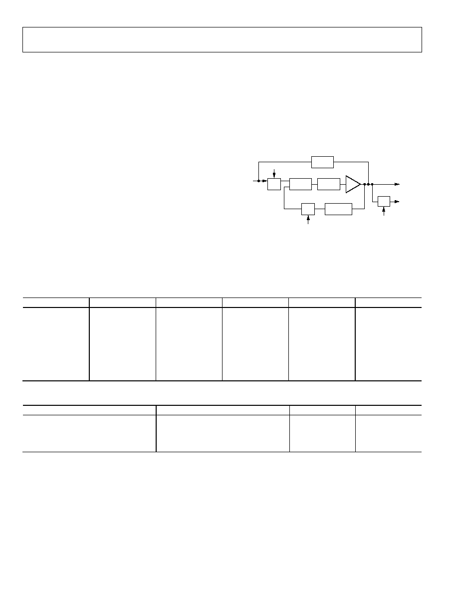
PLL
The ADV202 uses the PLL_HI and PLL_LO direct registers to
configure the PLL. Any time the PLL_LO register is modified,
the host must wait at least 20 µs before reading or writing any
other register. If this delay is not implemented, erratic behavior
might result.
The PLL can be programmed to have any possible final
multiplier value as long as
·
JCLK > 50 MHz and < 150 MHz (144-pin version).
·
JCLK > 50 MHz and < 115 MHz (121-pin version).
·
HCLK < 115 MHz.
·
JCLK 2 × VCLK for single-component input.
·
JCLK 2 × VCLK for YCrCb [4:2:2] input.
·
In JDATA mode (JDATA), JCLK must be 4 × MCLK or
higher.
·
The maximum burst frequency for external DMA modes is
0.36 JCLK.
·
For MCLK frequencies greater than 50 MHz, the input clock
divider must be enabled, that is, IPD set to 1.
·
IPD cannot be enabled for MCLK frequencies below 20 MHz.
To achieve the lowest power consumption, an MCLK frequency
of 27 MHz is recommended for a standard definition CCIR656
input. The PLL circuit is recommended to have a multiplier of 3.
This sets JCLK and HCLK to 81 MHz.
04723-009
LPF
PHASE
DETECT
VCO
JCLK
HCLK
÷
2
HCLKD
÷
PLLMULT
÷
2
LFB
÷
2
IPD
BYPASS
MCLK
Figure 24. PLL Architecture and Control Functions
Table 20. Recommended PLL Register Settings
IPD LFB PLLMULT
HCLKD
HCLK
JCLK
0
0
N
0
N × MCLK
N × MCLK
0
0
N
1
N × MCLK/2
N × MCLK
0
1
N
0
2 × N × MCLK
2 × N × MCLK
0
1
N
1
N × MCLK
2 × N × MCLK
1
0
N
0
N × MCLK/2
N × MCLK/2
1
0
N
1
N × MCLK/4
N × MCLK/2
1
1
N
0
N × MCLK
N × MCLK
1
1
N
1
N × MCLK/2
N × MCLK
Table 21. Recommended Values for PLL_HI and PLL_LO Registers
Video Standard
CLKIN Frequency on MCLK
PLL_HI
PLL_LO
SMPTE125M or ITU-R.BT656 (NTSC or PAL)
27 MHz
0x0008
0x0004
SMPTE293M (525p)
27 MHz
0x0008
0x0004
ITU-R.BT1358 (625p)
27 MHz
0x0008
0x0004
SMPTE274M (1080i)
74.25 MHz
0x0008
0x0084

ADV202
Rev. 0 | Page 31 of 40
HARDWARE BOOT
The boot mode can be configured via hardware using the CFG
pins or via software (see the ADV202 User's Guide). The first
boot mode after power-up is set by the CFG pins.
Only boot modes 2, 4, and 6, described in Table 22, are available
via hardware.
Table 22. Hardware Boot Modes
Boot Mode
Settings
Description
Hardware Boot
Mode 2
CFG<1> tied high,
CFG<2> tied low
No-Boot Host Mode. ADV202 does not boot, but all internal registers and memory are accessible
through normal host I/O operations.
For details, see the ADV202 User's Guide and the Getting Started with the ADV202 application note.
Hardware Boot
Mode 4
CFG<1> tied low,
CFG<2> tied high
SoC boot mode. The embedded software framework (ESF) takes control and establishes
communications with the host.
Hardware Boot
Mode 6
CFG<1> and <2>
tied high
SPI boot mode. Boot firmware over SPI from external flash memory.

ADV202
Rev. 0 | Page 32 of 40
VIDEO INPUT FORMATS
The ADV202 supports a wide variety of formats for
uncompressed video and still image data. The actual interface
and bus modes selected for transferring uncompressed data
dictates the allowed size of the input data and the number of
samples transferred with each access.
The host interface can support 8-, 10-, 12-, 14-, and 16-bit data
formats. The video interface can support video data or still
image data input/output. Supported formats are 8-, 10-, 12-, or
16-bit single or 2 × 8-bit, 2 × 10-bit, 2 × 12-bit multiplexed
formats. See the ADV202 User's Guide for details. All formats
can support less precision than provided by specifying the
actual data width/precision in the PMODE register.
The maximum allowable data input rate is limited by using
irreversible or reversible compression modes and the data width
(or precision) of the input samples. Use Table 23 and Table 24 to
determine the maximum data input rate.
Table 23. Maximum Pixel Data Input Rates
Interface
Compression
Mode
Input Format
Input Rate Limit
Active Resolution
(MSPS)
1
Approx Min Peak Output
Rate, Compressed Data
2
(Mbps)
Approx Max Output Rate,
Compressed Data
3
(Mbps)
144-PIN PACKAGE
HDATA
Irreversible
8-bit data
45
130
200
Irreversible
10-bit data
45
130
200
Irreversible
12-bit data
45
130
200
Irreversible
16-bit data
45
130
200
Reversible
8-bit data
40
130
200
Reversible
10-bit data
32
130
200
Reversible
12-bit data
27
130
200
Reversible
14-bit data
23
130
200
VDATA
Irreversible
8-bit data
65
130
200
Irreversible
10-bit data
65
130
200
Irreversible
12-bit data
65
130
200
Reversible
8-bit data
40
130
200
Reversible
10-bit data
32
130
200
Reversible
12-bit data
27
130
200
121-PIN PACKAGE
HDATA
Irreversible
8-bit data
34
98
150
Irreversible
10-bit data
34
98
150
Irreversible
12-bit data
34
98
150
Irreversible
16-bit data
34
98
150
Reversible
8-bit data
30
98
150
Reversible
10-bit data
24
98
150
Reversible
12-bit data
20
98
150
Reversible
14-bit data
17
98
150
VDATA
Irreversible
8-bit data
48
98
150
Irreversible
10-bit data
48
98
150
Irreversible
12-bit data
48
98
150
Reversible
8-bit data
30
98
150
Reversible
10-bit data
24
98
150
Reversible
12-bit data
20
98
150
1
Input rate limits for HDATA might be less for certain applications depending on input picture size and content, host interface settings, and DMA transfer settings.
2
Minimum peak output rate or guaranteed sustained output rate.
3
Maximum output rate, or output rate above this value is not possible.

ADV202
Rev. 0 | Page 33 of 40
Table 24. Maximum Supported Tile Width for Data Input on HDATA and VDATA Buses
Compression Mode
Input Format
Tile/Precinct Maximum Width
9/7i
Single-component
2048
9/7i
Two-component
1024 each
9/7i
Three-component
1024 (Y)
5/3i
Single-component
4096
5/3i
Two-component
2048 (each)
5/3i
Three-component
2048 (Y)
5/3r Single-component
4096
5/3r Two-component
2048
5/3r Three-component
1024
ADV202
Rev. 0 | Page 34 of 40
APPLICATIONS
This section describes typical video applications for the
ADV202 JPEG2000 video processor.
ENCODE--MULTICHIP MODE
Due to the data input rate limitation (see Table 23), an 1080i
application requires at least two ADV202s to encode or decode
full-resolution 1080i video. In encode mode, the ADV202
accepts Y and CbCr data on separate buses. The input data must
be in EAV/SAV format. An encode example is shown in
Figure 25.
In decode mode, a master/slave configuration (as shown in
Figure 26) or a slave/slave configuration can be used to
synchronize the outputs of the two ADV202s. See the ADV202
Multichip Application application note for details on how to
configure the ADV202s in a multichip application.
Applications that have two separate VDATA outputs sent to an
FPGA or buffer before they are sent to an encoder do not
require synchronization at the ADV202 outputs.
04723-002
DATA[31:0]
HDATA[31:0]
ADDR[3:0]
ADDR[3:0]
CS
CS
RD
RD
WR
WE
ACK
ACK
IRQ
CS
RD
WR
ACK
IRQ
DREQ
DACK
IRQ
DREQ
DREQ
FIELD
VSYNC
HSYNC
DACK
DACK
G I/O
SCOMM[5]
VCLK
1080i
VIDEO OUT
MCLK
VDATA[11:2]
32-BIT HOST CPU
ADV7402
10-BIT SD/HD
VIDEO
DECODER
ADV202
_1_SLAVE
SCOMM[5]
HDATA[31:0]
ADDR[3:0]
CS
RD
WE
ACK
IRQ
FIELD
VSYNC
HSYNC
DREQ
DACK
VCLK
MCLK
VDATA[11:2]
ADV202
_2_SLAVE
LLC
Y[9:0]
C[9:0]
CbCr
CbCr
Y
Figure 25. Encode--Multichip Application
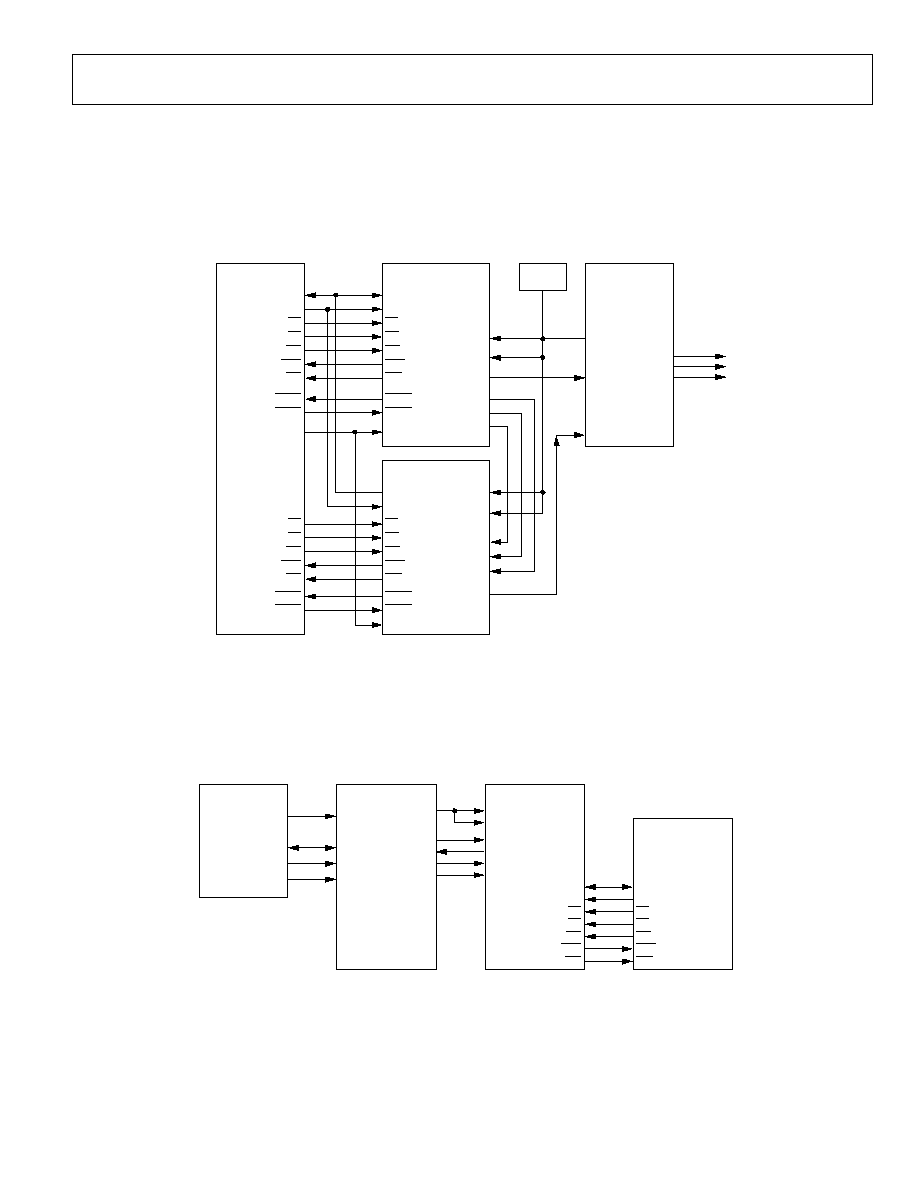
ADV202
Rev. 0 | Page 35 of 40
DECODE--MULTICHIP MASTER/SLAVE
In a master/slave configuration, it is expected that the master
HVF outputs are connected to the slave HVF inputs and that
each SCOMM[5] pin is connected to the same GPIO on the
host.
In a slave/slave configuration, the common HVF for both
ADV202s is generated by an external house sync and each
SCOMM[5] is connected to the same GPIO output on the host.
SWIRQ1, Software Interrupt 1 in the EIRQIE register, must be
unmasked on both devices to enable multichip mode.
04723-003
DATA[31:0]
HDATA[31:0]
ADDR[3:0]
ADDR[3:0]
CS
CS
RD
RD
WR
WE
ACK
ACK
IRQ
CS
RD
WR
ACK
IRQ
DREQ
DACK
IRQ
DREQ
DREQ
FIELD
VSYNC
HSYNC
DACK
DACK
G I/O
SCOMM[5]
VCLK
1080i
VIDEO OUT
MCLK
VDATA[11:2]
32-BIT HOST CPU
ADV730xA
10-BIT SD/HD
VIDEO
DECODER
ADV202
_1_MASTER
SCOMM[5]
HDATA[31:0]
ADDR[3:0]
CS
RD
WE
ACK
IRQ
FIELD
VSYNC
HSYNC
DREQ
DACK
VCLK
MCLK
VDATA[11:2]
ADV202
_2_SLAVE
CLKIN
Y[9:0]
C[9:0]
CbCr
CbCr
Y
Y
74.25MHz
OSC
Figure 26. Decode --Multichip Master/Slave Application
DIGITAL STILL CAMERA/CAMCORDER
Figure 27 is a typical configuration for a digital camera or camcorder.
04723-004
D[9:0]
10
DATA INPUTS[9:0]
MCLK
VCLK
VFRM
VRDY
VSTRB
VDATA[11:2]
SDATA
SERIAL DATA
SCK
SERIAL CLK
SL
SERIAL EN
AD9843A
FPGA
16-BIT
HOST CPU
ADV202
DATA[15:0]
HDATA[15:0]
ADDR[3:0]
ADDR[3:0]
CS
CS
RD
RD
WE
WE
ACK
ACK
IRQ
IRQ
Figure 27. Digital Still Camera/Camcorder Application
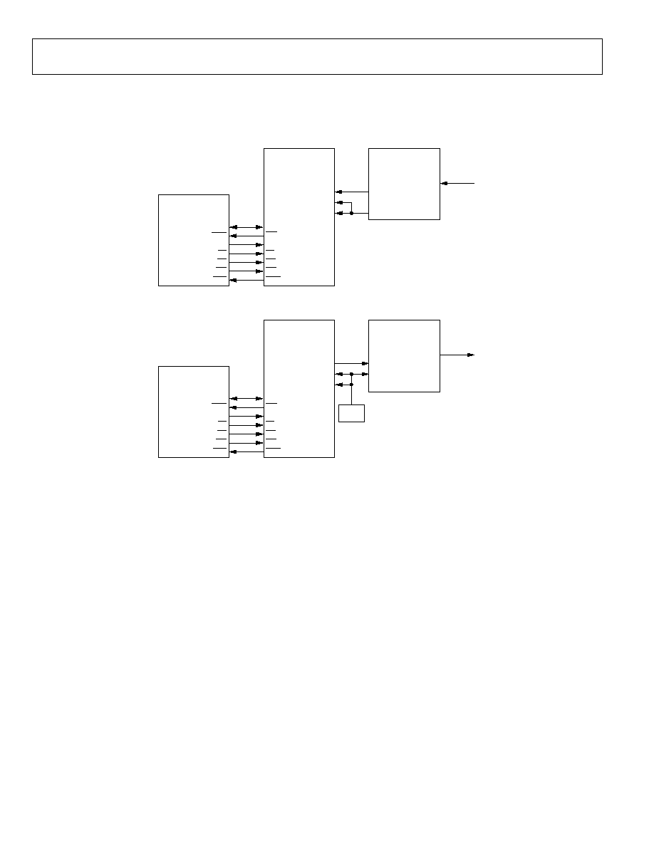
ADV202
Rev. 0 | Page 36 of 40
ENCODE/DECODE SDTV VIDEO APPLICATION
Figure 28 shows two ADV202 chips using 10-bit CCIR656 in normal host mode.
04723-005
ENCODE MODE
32-BIT
HOST CPU
ADV202
HDATA[31:0]
DATA[31:0]
ADV7189
10-BIT
VIDEO
DECODER
IRQ
INTR
ADDR[3:0]
ADDR[3:0]
P[19:10]
VDATA[11:2]
VIDEO IN
LLC1
VCLK
MCLK
CS
CS
RD
RD
WE
WE
ACK
ACK
27MHz
OSC
DECODE MODE
32-BIT
HOST CPU
ADV202
HDATA[31:0]
DATA[31:0]
ADV7301A
10-BIT
VIDEO
ENCODER
IRQ
INTR
ADDR[3:0]
ADDR[3:0]
P[9:0]
VDATA[11:2]
VIDEO OUT
CLKIN
VCLK
MCLK
CS
CS
RD
RD
WE
WE
ACK
ACK
Figure 28. Encode/Decode--SDTV Video Application

ADV202
Rev. 0 | Page 37 of 40
ASIC APPLICATION (32-BIT HOST/32-BIT ASIC)
Figure 29 shows two ADV202 chips using 10-bit CCIR656 in normal host mode.
04723-006
ENCODE MODE
32-BIT
HOST CPU
ADV202
DATA[31:0]
IRQ
IRQ
ADDR[3:0]
ADDR[3:0]
CS
CS
RD
RD
WE
WE
ACK
ACK
ASIC
ADV7189
10-BIT
VIDEO
DECODER
P[19:10]
LLC1
VDATA[11:2]
VIDEO IN
VCLK
MCLK
DREQ0
DREQ0
DACK0
DACK0
HDATA[31:0]
DATA[31:0]
27MHz
OSC
DECODE MODE
31 -BIT
HOST CPU
ADV202
DATA[31:0]
IRQ
IRQ
ADDR[3:0]
ADDR[3:0]
CS
CS
RD
RD
WE
WE
ACK
ACK
ASIC
ADV730xA
10-BIT
VIDEO
ENCODER
P[9:0]
VDATA[11:2]
VIDEO OUT
CLKIN
VCLK
MCLK
DREQ0
DREQ0
DACK0
DACK0
HDATA[31:0]
DATA[31:0]
Figure 29. Encode/Decode ASIC Application
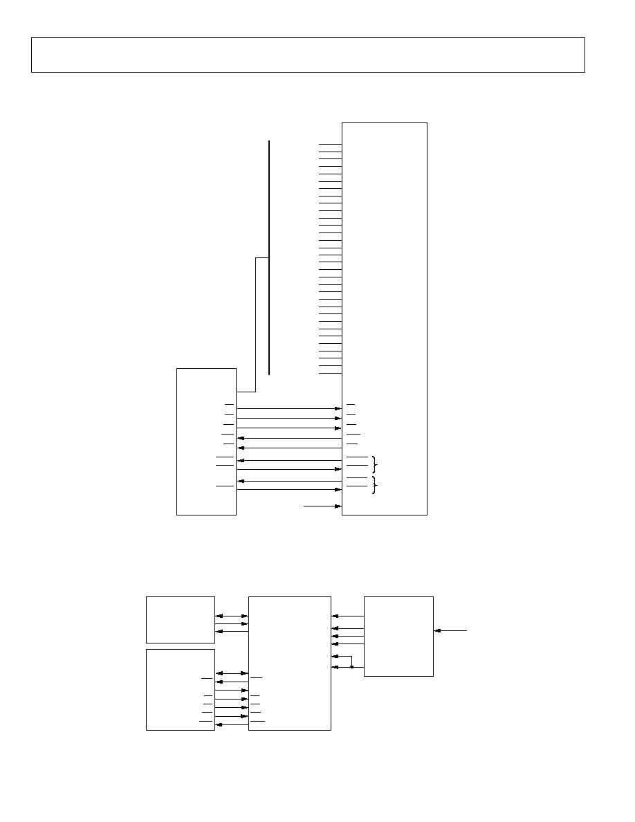
ADV202
Rev. 0 | Page 38 of 40
HIPI (HOST INTERFACE--PIXEL INTERFACE)
Figure 30 is a typical configuration using HIPI mode.
04723-007
HDATA<31>
Y0/G0<MSB>
HDATA<30>
Y0/G0<6>
HDATA<29>
Y0/G0<5>
HDATA<28>
Y0/G0<4>
HDATA<27>
Y0/G0<3>
HDATA<26>
Y0/G0<2>
HDATA<25>
Y0/G0<1>
HDATA<24>
Y0/G0<0>
HDATA<23>
Cb0/G1<MSB>
HDATA<22>
Cb0/G1<6>
HDATA<21>
Cb0/G1<5>
HDATA<20>
Cb0/G1<4>
HDATA<19>
Cb0/G1<3>
HDATA<18>
Cb0/G1<2>
HDATA<17>
Cb0/G1<1>
HDATA<16>
Cb0/G1<0>
HDATA<15>
Y1/G2<MSB>
HDATA<14>
Y1/G2<6>
HDATA<13>
Y1/G2<5>
HDATA<12>
Y1/G2<4>
HDATA<11>
Y1/G2<3>
HDATA<10>
Y1/G2<2>
HDATA<9>
Y1/G2<1>
HDATA<8>
Y1/G2<0>
HDATA<7>
Cr0/G3<MSB>
HDATA<6>
Cr0/G3<6>
HDATA<5>
Cr0/G3<5>
HDATA<4>
Cr0/G3<4>
HDATA<3>
Cr0/G3<3>
HDATA<2>
Cr0/G3<2>
HDATA<1>
Cr0/G3<1>
HDATA<0>
Cr0/G3<0>
CS
DATA<31:0>
CS
RD
RD
WR
WE
ACK
ACK
IRQ
IRQ
DREQ
DREQ0
DACK
DACK0
MCLK
74.25MHz
DREQ
DREQ1
DACK
DACK1
ADV202
32-BIT HOST
RAW PIXEL
DATAPATH
COMPRESSED
DATAPATH
Figure 30. Host Interface--Pixel Interface mode
JDATA INTERFACE
Figure 31 shows a typical configuration using JDATA with a dedicated JDATA output, 16-bit host, and 10-bit CCIR656.
04723-008
16-BIT
HOST CPU
ASIC
ADV202
HDATA[15:0]
DATA[15:0]
ADV7189
IRQ
IRQ
ADDR[3:0]
ADDR[3:0]
P[19:10]
VDATA[11:2]
FIELD
FIELD
VS
VSYNC
HS
LLC1
HSYNC
VCLK
MCLK
VIDEO IN
YCrCb
CS
CS
JDATA[7:0]
HOLD
VALID
RD
RD
WE
WE
ACK
ACK
Figure 31. JDATA Application

ADV202
Rev. 0 | Page 39 of 40
OUTLINE DIMENSIONS
SEATING
PLANE
DETAILA
0.70
0.60
0.50
BALL DIAMETER
0.20 NOM
COPLANARITY
1.00 BSC
10.00
BSC SQ
A
B
C
D
E
F
G
H
J
K
L
10
8 7 6
3 2 1
9
5 4
11
1.31*
1.21
1.11
A1 CORNER
INDEX AREA
TOP VIEW
BALL A1
INDICATOR
DETAIL A
BOTTOM VIEW
0.50 NOM
0.30 MIN
1.85*
1.71
1.40
COMPLIANT WITH JEDEC STANDARDS MO-192-ABD-1
EXCEPT FOR DIMENSIONS INDICATED BY A "*" SYMBOL
12.20
12.00 SQ
11.80
Figure 32. 121-Lead Chip Scale Ball Grid Array [CSPBGA]
(BC-121)
Dimensions shown in millimeters
SEATING
PLANE
DETAILA
0.70
0.60
0.50
BALL DIAMETER
COPLANARITY
0.20 MAX
1.00 BSC
11.00
BSC
A
B
C
D
E
F
G
J
H
K
L
M
12 11 10
8 7 6
3 2 1
9
5 4
0.53
0.43
A1 CORNER
INDEX AREA
TOP VIEW
13 .00
BSC SQ
BALL A1
INDICATOR
DETAIL A
BOTTOM VIEW
*1.85
MAX
*1.32
1.21
1.11
COMPLIANT WITH JEDEC STANDARDS MO-192-AAD-1
EXCEPT FOR DIMENSIONS INDICATED BY A "*" SYMBOL
Figure 33. 144-Lead Chip Scale Ball Grid Array [CSPBGA]
(BC-144-3)
Dimensions shown in millimeters

ADV202
Rev. 0 | Page 40 of 40
ORDERING GUIDE
Model
Temperature
Range
Speed
Grade
Operating Voltage
Package Description
Package
Option
ADV202BBC-115
40°C to +85°C
115 MHz
1.5 V internal, 2.5 V or 3.3 V I/O
121-Lead CSPBGA
BC-121
ADV202BBCZ-115
1
40°C to +85°C
115 MHz
1.5 V internal, 2.5 V or 3.3 V I/O
121-Lead CSPBGA
BC-121
ADV202BBC-150
40°C to +85°C
150 MHz
1.5 V internal, 2.5 V or 3.3 V I/O
144-Lead CSPBGA
BC-144-3
ADV202BBCZ-150
1
40°C to +85°C
150 MHz
1.5 V internal, 2.5 V or 3.3 V I/O
144-Lead CSPBGA
BC-144-3
ADV202-HD-EB
High Definition Evaluation Board
ADV202-SD-EB
Standard Definition Evaluation
Board
1
Z = Pb-free part.
© 2004 Analog Devices, Inc. All rights reserved. Trademarks and
registered trademarks are the property of their respective owners.
D0472307/04(0)