ADuC7020/ADuC7021/ADuC7022 Precision Analog Microcontroller Small Package, 12-bit Analog I/O, ARM7TDMI® MCU Preliminary Data sheet (REV. PrC)
Precision Analog Microcontroller
Small Package, 12-bit Analog I/O, ARM7TDMI® MCU
Preliminary Technical Data
ADuC7020/ADuC7021/ADuC7022
FEATURES
Analog I/O
Multi-Channel, 12-bit, 1MSPS ADC
- 5 Channels on the ADuC7020
- 8 Channels on the ADuC7021
- 10 Channels on the ADuC7022
Differential and single-ended modes
0 to Vref Analog Input Range
Multi-Channel 12-bit Voltage Output DACs
- 4 Outputs on the ADuC7020
- 2 Outputs on the ADuC7021
On-Chip 20ppm/°C Voltage Reference
On-Chip Temperature Sensor (±3°C)
Uncommitted Voltage Comparator
Microcontroller
ARM7TDMI Core, 16/32-bit RISC architecture
JTAG Port supports code download and debug
Clocking options: - Trimmed On-Chip Oscillator (± 2%)
- External Watch crystal
- External clock source
45MHz PLL with Programmable Divider
Memory
62k Bytes Flash/EE Memory, 8k Bytes SRAM
In-Circuit Download, JTAG based Debug
Software triggered in-circuit re-programmability
On-Chip Peripherals
UART, dual I
2
C and SPI Serial I/O
14-Pin GPIO Port
2 X General Purpose Timers
Wake-up and Watchdog Timers
Power Supply Monitor
PLA Programmable Logic (Array)
Power
Specified for 3V operation
Active Mode: 6mW (@1MHz)
300mW (@45MHz)
Packages and Temperature Range
40 Pin LFCSP 6x6mm body package
Fully specified for 40°C to 85°C operation
Tools
Low-Cost QuickStart Development System
Full Third-Party Support
APPLICATIONS
Optical Networking Laser Power Control
Base Station Systems
Precision Instrumentation, Smart Sensors
Optical Transceivers Digital Diagnostic Monitoring
(See general description on page 10)
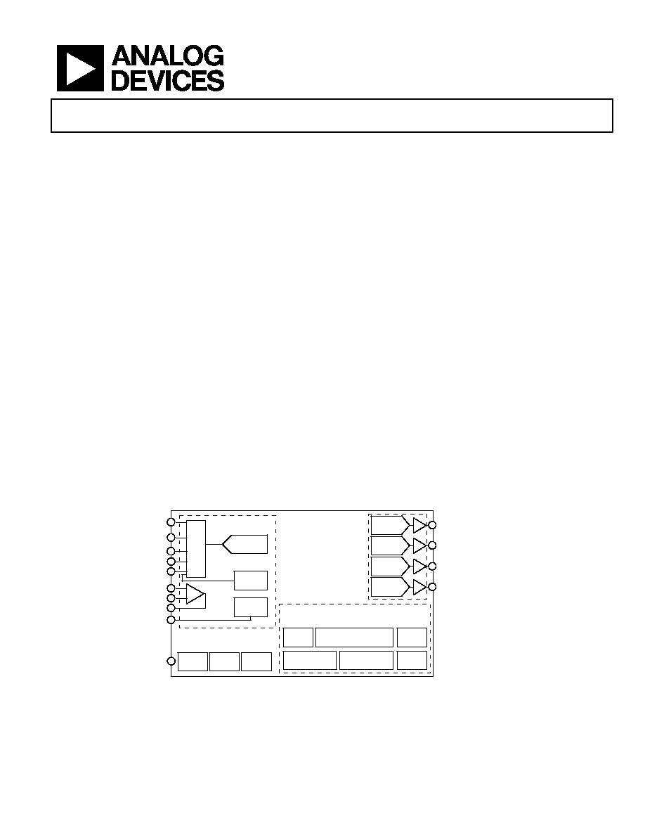
FUNCTIONAL BLOCK DIAGRAM
1MSPS
12-BIT ADC
MUX
TEMP
SENSOR
ADC0
+
-
CMP0
CMP1
CMP
OUT
V
REF
BANDGAP
REF
ADC5*
..
.
..
.
ADC9**
ARM7TDMI-BASED MCU WITH
ADDITIONAL PERIPHERALS
2kX32 SRAM
31kX16 FLASH/EEPROM
GPIO
JTAG
4 GEN. PUR-
POSE TIMERS
SERIAL I/O
UART, SPI, 2xI2C
PLA
RST
POR
OSC
& PLL
PSM
ADuC7020
ADuC7021
ADuC7022
* not on the ADuC7020
** ADuC7022 only
*** not on the ADuC7022
**** ADuC7020 only
DAC0***
12-BIT DAC
DAC3****
12-BIT DAC
DAC2****
12-BIT DAC
DAC1***
12-BIT DAC
ADC7*
ADC8**
..
.
..
.
Figure 1
Rev. PrC
Information furnis hed by Analog Devices is believed to be accurate and reliable.
However, no res pons ibility is as s umed by Analog Devices for its us e, nor for any
infringements of patents or other rights of third parties that may result from its use.
Specifications subject to change without notice. No license is granted by implication
or otherwise under any patent or patent rights of Analog Devices. Trademarks and
registered trademarks are the property of their respective companies.
One Technology Way, P.O. Box 9106, Norwood, MA 02062-9106, U.S.A.
Tel: 781.329.4700
www.analog.com
Fax: 781.326.8703
© 2004 Analog Devices, Inc. All rights reserved.

ADuC7020/ADuC7021/ADuC7022
Preliminary Technical Data
Rev. PrC | Page 2 of 16
TABLE OF CONTENTS
ADuC7020/21/22--Specifications ................................................. 3
Absolute Maximum Ratings............................................................ 7
Ordering Guide............................................................................. 7
Pin function descriptions ................................................................ 8
General Description ....................................................................... 10
Overview of the ARM7TDMI core.......................................... 10
Memory organisation ................................................................ 11
Outline Dimensions ....................................................................... 16

Preliminary Technical Data
ADuC7020/ADuC7021/ADuC7022
Rev. PrC | Page 3 of 16
ADUC7020/21/22--SPECIFICATIONS
1
Table 1. (AV
DD
= IOV
DD
= 2.7 to 3.6V, V
REF
= 2.5 V Internal Reference, f
CORE
= 45MHz, All specifications T
A
= T
MAX
to T
MIN
, unless otherwise noted.)
Parameter
ADuC7020/21/22
Unit
Test Conditions/Comments
ADC CHANNEL SPECIFICATIONS
DC Accuracy
2, 3
f
SAMPLE
= 1MSPS
Resolution
12
Bits
Integral Nonlinearity
Integral Nonlinearity
4
±1.5
±0.5
±2.0
LSB max
LSB typ
LSB max
2.5V internal reference
2.5V internal reference
1.0V external reference
Differential Nonlinearity
Differential Nonlinearity
4
DC Code Distribution
+1/-0.9
±0.5
+1/-0.9
1
LSB max
LSB typ
LSB max
LSB typ
2.5V internal reference
2.5V internal reference
1.0V external reference
ADC input is a dc voltage
CALIBRATED ENDPOINT ERRORS
5
Offset Error
Offset Error Match
±5
±1
LSB max
LSB typ
Gain Error
Gain Error Match
±5
±1
LSB max
LSB typ
DYNAMIC PERFORMANCE
Fin = 10kHz Sine Wave, f
SAMPLE
= 1MSPS
Signal-to-Noise Ratio (SNR)
6
71
dB typ
Total Harmonic Distortion (THD)
-78
dB typ
Peak Harmonic or Spurious Noise
Channel-to-Channel Crosstalk
7
-78
-80
dB typ
dB typ
ANALOG INPUT
Input Voltage Ranges
Differential mode
V
CM
8
±V
REF
/2
Volts
Single-ended mode
0 to V
REF
Volts
Leakage Current
±5
µA max
Input Capacitance
20
pF typ
During ADC Acquisition
ON-CHIP VOLTAGE REFERENCE
Output Voltage
2.5
V
0.47µF from V
REF
(pin 55) to AGND
Accuracy
±10
mV max
Measured at T
A
= 25°C
Reference Temperature Coefficient
Power Supply Rejection Ratio
±10
80
ppm/°C typ
dB typ
Output Impedance
Internal V
REF
Power-On Time
10
1
typ
ms typ
EXTERNAL REFERENCE INPUT
9
Input Voltage Range
Input Impedance
0.625
AV
DD
TBD
V min
V max
K typ
DAC CHANNEL SPECIFICATIONS
R
L
= 5k
, C
L
= 100pF
DC ACCURACY
Resolution
12
Bits
Relative Accuracy
±2
LSB typ
Differential Nonlinearity
±1
LSB max
Guaranteed Monotonic
Offset Error
±2
±5
mV max
mV max
DAC output unbuffered
DAC output buffered
Gain Error
Gain Error Mismatch
±0.5
TBD
% max
% typ
% of fullscale on DAC0

ADuC7020/ADuC7021/ADuC7022
Preliminary Technical Data
Rev. PrC | Page 4 of 16
Parameter
ADuC7020/21/22
Unit
Test Conditions/Comments
ANALOG OUTPUTS
Output Voltage Range_0
Ouput Voltage Range_1
Output Voltage Range_2
0 to DACREF
0 to 2.5V
0 to DACV
DD
V typ
V typ
V typ
DACREF range: DACGND to DACV
DD
Output Impedance
10
typ
DAC AC CHARACTERISTICS
Voltage Output Settling Time
Voltage Output Settling Time
Digital to Analog Glitch Energy
10
15
TBD
µs typ
µs typ
nV-sec typ
DAC Output buffered
DAC Output unbuffered
I LSB change at major carry
COMPARATOR
Input Offset Voltage
Input Bias Current
Input Voltage Range
Input Capacitance
Hysteresis
Response Time
±10
5
AV
DD
-1.2
7
5
10
1
10
mV
nA typ
V max
pF typ
mV min
mv max
µs min
µs max
Hysteresis can be turned on or off via the CMPHYST
bit in the CMPCON register
Response time may be modified via the CMPRES bits
in the CMPCON register
TEMPERATURE SENSOR
Voltage Output at 25°C
Voltage TC
TBD
-2.0
mV typ
mV/°C typ
Accuracy
±3
°C typ
POWER SUPPLY MONITOR (PSM)
IOV
DD
Trip Point Selection
2.79
V
Two selectable Trip Points
3.07
V
Power Supply Trip Point Accuracy
±2.5
% max
Of the selected nominal Trip Point Voltage
Watchdog Timer (WDT)
4
Timeout Period
0
TBD
ms min
ms max
Flash/EE MEMORY
Endurance
10
10,000
Cycles min
Data Retention
11
30
Years min
T
J
= 55°C
Digital Inputs
Input Leakage Current
Input Capacitance
±10
±1
10
µA max
µA typ
pF typ
All digital inputs including XTAL1 and XTAL2
Logic Inputs
4
VINL, Input Low Voltage
VINH, Input High Voltage
0.4
2.0
V max
V min
All Logic inputs including XTAL1 and XTAL2
Logic Outputs
VOH, Output High Voltage
2.4
V min
I
SOURCE
= 20µA
VOL, Output Low Voltage
0.4
V max
I
SINK
= 1.6mA
MCU CLOCK RATE
355.5
45.5
kHz min
MHz max
8 programmable core clock selections within this
range
STARTUP TIME
At Power-On
From Idle Mode
From Power-Down Mode
TBD
TBD
TBD
Core Clock = TBD MHz
Programmable Logic Array (PLA)
Propagation Delay
TBD
ns typ
From input pin to output pin

Preliminary Technical Data
ADuC7020/ADuC7021/ADuC7022
Rev. PrC | Page 5 of 16
Parameter
ADuC7020/21/22
Unit
Test Conditions/Comments
POWER REQUIREMENTS
12
,
13
Power Supply Voltage Range
AV
DD
AGND and IOV
DD
- IOGND
2.7
V min
3.6
V max
Power Supply Current Normal Mode
3mA
5
50
mA typ
mA max
mA typ
1MHz clock
1MHz clock
45MHz clock
60
mA max
45MHz clock
Power Supply Current Idle Mode
Power Supply Current Power Down
Mode
1
30
100
mA max
µA typ
µA max
External Crystal or Internal Osc ON
External Crystal or Internal Osc ON
1
Temperature Range -40° to +85°C
2
All ADC Channel Specifications are guaranteed during normal MicroConverter core operation.
3
These specification apply to all ADC input channels.
4
These numbers are not production tested but are supported by design and/or characterization data on production release.
5
Based on external ADC system components, the user may need to execute a system calibration to remove external endpoint and achieve these specifications..
6
SNR calculation includes distortion and noise components.
7
Channel-to-channel crosstalk is measured on adjacent channels.
8
The input signal can be centered on any dc common-mode voltage (V
CM
) as long as this value is within the ADC voltage input range specified.
9
When using an external reference input pin, the internal reference must be disabled by setting the lsb in the REFCON Memeory Mapped Register to 0.
10
Endurance is qualified to 50,000 cycles as per JEDEC Std. 22 method A117 and measured at -40°C, +25°C and +85°C. Typical endurance at 25°C is 70,000 cycles.
11
Retention lifetime equivalent at junction temperature (Tj) = 55°C as per JEDEC Std. 22 method A117. Retention lifetime will derate with junction temperature.
12
Power supply current consumption is measured in normal, idle and power-down modes under the following conditions:
Normal Mode:
TBD
Idle Mode:
TBD
Power-Down:
TBD
13
DV
DD
power supply current increases typically by TBD mA during a Flash/EE memory program or erase cycle.
Document Outline