Äîêóìåíòàöèÿ è îïèñàíèÿ www.docs.chipfind.ru
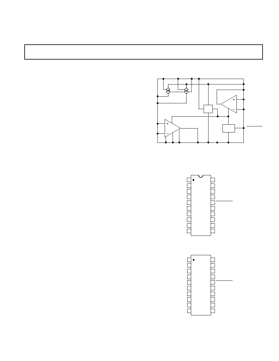
FUNCTIONAL BLOCK DIAGRAM
RGA RGB
IN
IA
+IN
IA
INST
AMP
SHUT-
DOWN
GND
SENSE
OUT
IA
AGND
DGND
V
S
SHUTDOWN
+IN
OA
IN
OA
OUT
OA
+V
S
2.5V
REF
I
OUTA
I
OUTB
MATCHED
CURRENT
SOURCES
NULLA
NULLB
BIAS 2.5V
REFOUT
ADT70
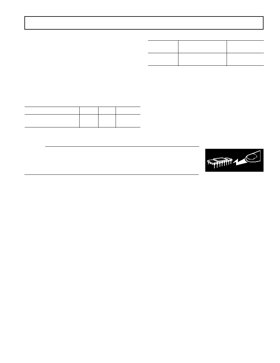
PIN CONFIGURATIONS
20-Lead P-DIP
(N Suffix)
SHUTDOWN
14
13
12
11
17
16
15
20
19
18
10
9
8
1
2
3
4
7
6
5
V
S
+IN
OA
IN
OA
V
OUT
OA
+V
S
AGND
V
REFOUT
BIAS
V
OUT
IA
DGND
NULLA
NULLB
I
OUTA
I
OUTB
IN
IA
+IN
IA
RGA
RGB
GND SENSE
a
ADT70
TOP VIEW
(Not to Scale)
20-Lead SOIC
(R Suffix)
14
13
12
11
17
16
15
20
19
18
10
9
8
1
2
3
4
7
6
5
V
S
+IN
OA
IN
OA
V
OUT OA
+V
S
AGND
V
REFOUT
BIAS
V
OUT
IA
DGND
SHUTDOWN
NULLA
NULLB
I
OUTA
I
OUTB
IN
IA
IN
IA
RGA
RGB
GND SENSE
ADT70
TOP VIEW
(Not to Scale)
a
REV. 0
Information furnished by Analog Devices is believed to be accurate and
reliable. However, no responsibility is assumed by Analog Devices for its
use, nor for any infringements of patents or other rights of third parties
which may result from its use. No license is granted by implication or
otherwise under any patent or patent rights of Analog Devices.
a
PRTD Conditioning Circuit
and Temperature Controller
ADT70*
FEATURES
PRTD Temperature Measurement Range
Typical IC Measurement Error 1 C
Includes Two Matched Current Sources
Rail-to-Rail Output Instrumentation Amp
Uncommitted, Rail-to-Rail Output Op Amp
On-Board 2.5 V Reference
Temperature Coefficient 25 ppm/ C
5 V or 5 V Operation
Supply Current 4 mA Max
10 A Max in Shutdown
APPLICATIONS
Temperature Controllers
Portable Instrumentation
Temperature Acquisition Cards
GENERAL DESCRIPTION
The ADT70 provides excitation and signal conditioning for
resistance-temperature devices (RTDs). It is ideally suited for
1 k
Platinum RTDs (PRTDs), allowing a very wide range of
temperature measurement. It can also easily interface to 100
PRTDs. Using a remote, low cost thin-film PRTD, the ADT70
can measure temperature in the range of 50
°
C to +500
°
C.
With high performance platinum elements, the temperature
change can be extended to 1000
°
C. Accuracy of the ADT70
and PRTD system over a 200
°
C to +1000
°
C temperature
range heavily depends on the quality of the PRTD. Typically
the ADT70 will introduce an error of only
±
1
°
C over the
transducer's temperature range, and the error may be trimmed
to zero at a single calibration point.
The ADT70 consists of two matched 1 mA (nominal) current
sources for transducer and reference resistor excitation, a preci-
sion rail-to-rail output instrumentation amplifier, a 2.5 V refer-
ence and an uncommitted rail-to-rail output op amp. The
ADT70 includes a shutdown function for battery powered
equipment, which reduces the quiescent current from 4 mA to
less than 10
µ
A. The ADT70 operates from either single +5 V
or
±
5 V supplies. Gain or full-scale range for the PRTD and
ADT70 system is set by a precision external resistor connected
to the instrumentation amplifier. The uncommitted op amp may
be used for scaling the internal voltage reference, providing a
"PRTD open" signal or "over-temperature" warning, a heater
switching signal, or other external conditioning determined by
the user.
The ADT70 is specified for operation from 40
°
C to 125
°
C
and is available in 20-lead DIP and SO packages.
*
Patent pending.
One Technology Way, P.O. Box 9106, Norwood, MA 02062-9106, U.S.A.
Tel: 781/329-4700
World Wide Web Site: http://www.analog.com
Fax: 781/326-8703
© Analog Devices, Inc., 1998

Parameter
Symbol
Conditions
Min
Typ
Max
Units
SYSTEM CONFIGURATION
Gain
R
L
= 1 k
1.234
1.295
1.364
mV/
Line Regulation
2.25
0.35
2.25
%/V
CURRENT SOURCES
Output Current
I
Q1
, I
Q2
R
L
= 1 k
0.9
mA
Output Current Mismatch
I
Q1
I
Q2
R
L
= 1 k
2
0.5
2
µ
A
Voltage Compliance
V
S
to +V
S
1.5
V
INSTRUMENTATION AMP
Input Offset Voltage
V
IOS
700
150
700
µ
V
T
A
= +25
°
C
500
100
500
µ
V
Output Offset Voltage
V
OOS
12
5
12
mV
T
A
= +25
°
C
7
3
7
mV
Input Bias Current
I
B
75
40
75
nA
T
A
= +25
°
C
60
30
60
nA
Input Offset Current
I
OS
3
1
3
nA
Common-Mode Rejection
CMR
V
CM
= 0.5 V to 3 V
65
85
dB
Output Voltage Swing
V
OUT
R
L
=
, V
S
= 5 V
V
S
+ 25
+V
S
25
mV
Power Supply Rejection Ratio
PSRR
+ 4.5 V
V
S
5.5 V
2.5
0.5
2.5
mV/V
VOLTAGE REFERENCE
Output Voltage
2.485
2.5
2.515
V
T
A
= +25
°
C
2.49
2.5
2.51
V
Load Regulation
I
L
= 0 mA to 1 mA
250
ppm/mA
Temperature Coefficient
10
ppm/
°
C
Line Regulation
+ 4.5 V
V
S
+5.5 V
75
ppm/V
OPERATIONAL AMPLIFIER
Input Offset Voltage
V
IOA
1,000
400
1,000
µ
V
T
A
= +25
°
C
800
200
800
µ
V
Input Offset Voltage Drift
T
C
V
IOA
1
µ
V/
°
C
Input Bias Current
I
B
75
40
75
nA
T
A
= +25
°
C
60
30
60
nA
Input Offset Current
I
OS
3
1
3
nA
Open-Loop Voltage Gain
A
VOL
R
L
=
2
V/
µ
V
Output Voltage Swing
V
OUTA
R
L
=
V
S
+ 10
+V
S
10
mV
Common-Mode Rejection Ratio
CMRR
V
CM
= 1 V to 4 V
85
105
dB
T
A
= +25
°
C
88
110
dB
Power Supply Rejection Ratio
PSRR
3 V
V
S
6 V
100
150
dB
Slew Rate
SR
T
A
= +25
°
C, A
V
= 1,
0.17
V/
µ
s
V
IN
= 0 V to 4 V
SHUTDOWN INPUT
Input Low Voltage
V
IL
0.8
V
Input High Voltage
V
IH
2.4
V
POWER SUPPLY
Supply Current
I
SY
R
L
= 1 k
3.5
5
mA
Shutdown Supply Current
I
SD
10
30
µ
A
Supply Voltage
V
S
+4.5
+5.5
V
Dual Supply Voltage
4.5
5.5
V
Specifications subject to change without notice.
ADT70SPECIFICATIONS
REV. 0
2
(V
S
= 5 V, 40 C
T
A
125 C unless otherwise noted)
ADT70
REV. 0
3
ORDERING GUIDE
Temperature
Model
Range
Package
ADT70GR
40
°
C to 125
°
C
20-Lead SOIC
ADT70GN
40
°
C to 125
°
C
20-Lead PDIP
ABSOLUTE MAXIMUM RATINGS*
Supply Voltage . . . . . . . . . . . . . . . . . . . . . . . . . . . . . . . .
16 V
Output Short-Circuit Duration . . . . . . . . . . . . . . . . . Indefinite
Storage Temperature Range
N, R Package . . . . . . . . . . . . . . . . . . . . . .
65
°
C to 150
°
C
Operating Temperature Range . . . . . . . . . .
40
°
C to 125
°
C
Junction Temperature Range
N, R Package . . . . . . . . . . . . . . . . . . . . . .
65
°
C to 125
°
C
Lead Temperature (Soldering, 60 sec) . . . . . . . . . . . .
300
°
C
NOTE
*Stresses above those listed under Absolute Maximum Ratings may cause perma-
nent damage to the device. This is a stress rating only; functional operation of the
device at these or any other conditions above those listed in the operational sections
of this specification is not implied. Exposure to absolute maximum rating condi-
tions for extended periods may affect device reliability.
Package Type
JA
*
JC
Units
20-Lead SOIC (R)
74
24
°
C/W
20-Lead PDIP (N)
102
31
°
C/W
NOTE
*
JA
is specified for device in socket/soldered on circuit board (worst case conditions).
TRANSISTOR COUNT: 158
CAUTION
ESD (electrostatic discharge) sensitive device. Electrostatic charges as high as 4000 V readily
accumulate on the human body and test equipment and can discharge without detection.
Although the ADT70 features proprietary ESD protection circuitry, permanent damage may
occur on devices subjected to high energy electrostatic discharges. Therefore, proper ESD
precautions are recommended to avoid performance degradation or loss of functionality.
WARNING!
ESD SENSITIVE DEVICE
ADT70
REV. 0
4
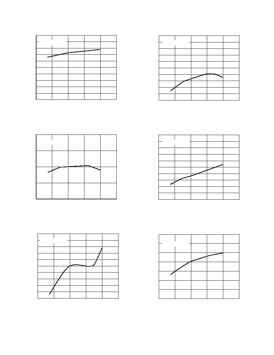
TEMPERATURE C
5
4
0
SUPPLY CURRENT mA
3
2
1
25
25
75
125
0.5
1.5
2.5
3.5
4.5
V
S
= +5V, NO LOAD
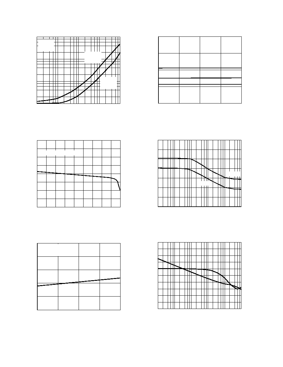
Figure 1. Supply Current vs. Temperature
TEMPERATURE C
SYSTEM GAIN mV/
25
25
75
125
1.2
1.25
1.3
V
S
= +5V, NO LOAD
1.4
1.35
Figure 2. System Gain vs. Temperature
TEMPERATURE C
SYSTEM GAIN PSRR %/V
25
25
75
125
0.06
V
S
= +5V, NO LOAD
0.08
0.1
0.04
0.02
0
0.02
0.04
0.06
0.08
0.1
Figure 3. Total System Gain PSRR vs. Temperature
TEMPERATURE C
INSTRUMENTATION AMPLIFIER INPUT
OFFSET VOLTAGE
V
25
25
75
125
60
V
S
= +5V, NO LOAD
80
100
40
20
0
20
40
60
80
100
Figure 4. Instrumentation Amplifier Input Offset Voltage
vs. Temperature
TEMPERATURE C
INSTRUMENTATION AMPLIFIER OUTPUT
OFFSET VOLTAGE mV
25
25
75
125
6
V
S
= +5V, NO LOAD
8
10
4
2
0
2
4
6
8
10
Figure 5. Instrumentation Amplifier Output Offset Voltage
vs. Temperature
TEMPERATURE C
INSTRUMENTATION AMPLIFIER INPUT
BIAS CURRENT nA
25
25
75
125
V
S
= +5V, NO LOAD
70
60
0
50
40
30
20
10
Figure 6. Instrumentation Amplifier Input Bias Current vs.
Temperature
ADT70
REV. 0
5
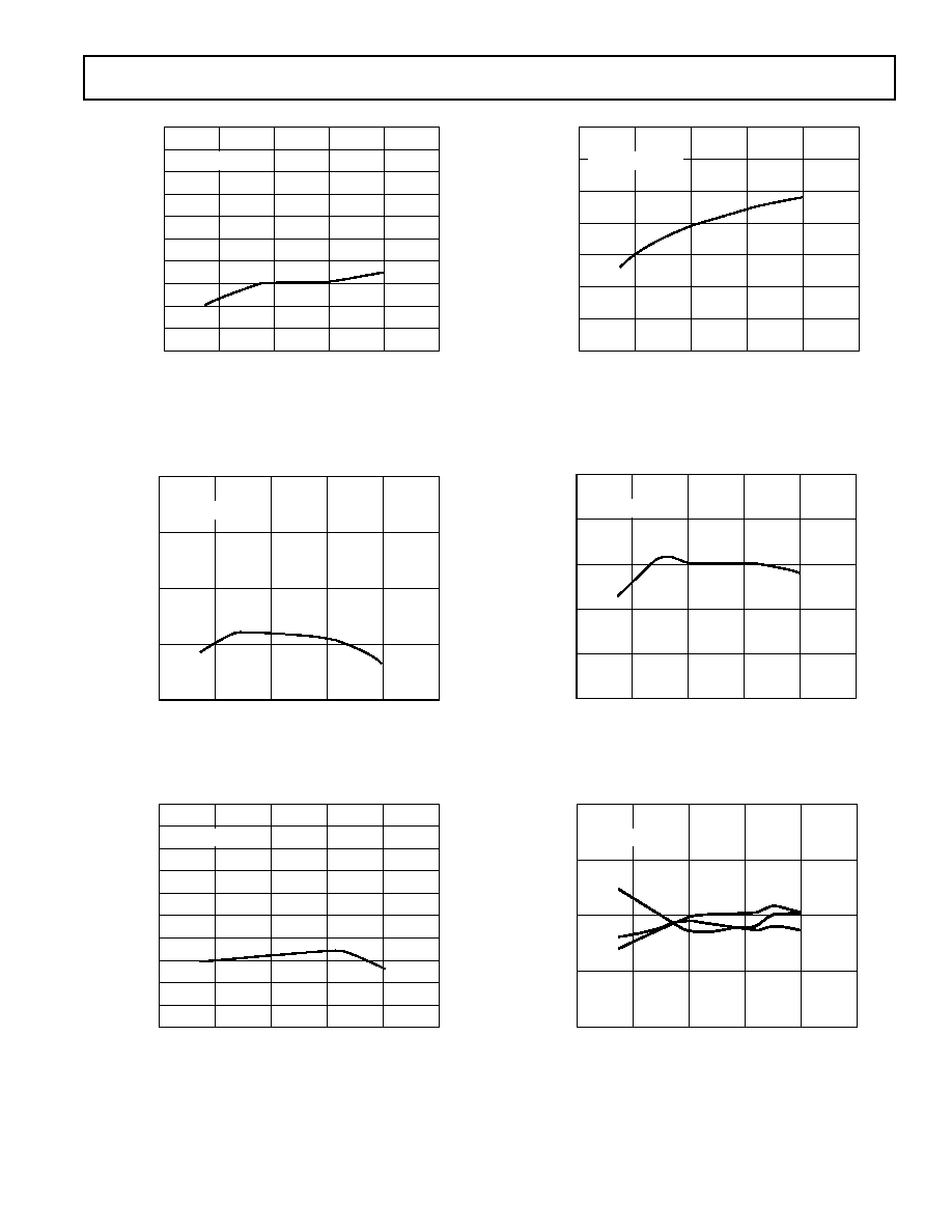
TEMPERATURE C
INSTRUMENTATION AMPLIFIER INPUT
OFFSET CURRENT pA
25
25
75
125
300
V
S
= +5V, NO LOAD
400
500
200
100
500
0
100
200
300
400
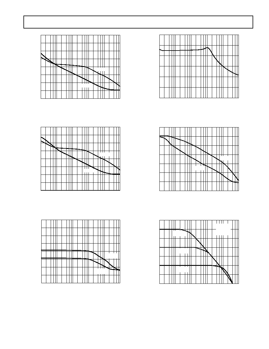
Figure 7. Instrumentation Amplifier Input Offset Current
vs. Temperature
TEMPERATURE C
INSTRUMENTATION AMPLIFIER GAIN V/V
25
25
75
125
1.45
V
S
= +5V, NO LOAD
1.4
1.5
1.55
1.6
Figure 8. Instrumentation Amplifier Gain vs. Temperature
TEMPERATURE C
OP AMP INPUT OFFSET VOLTAGE
V
25
25
75
125
60
V
S
= +5V, NO LOAD
80
100
40
20
100
0
20
40
60
80
Figure 9. Op Amp Input Offset Voltage vs. Temperature
TEMPERATURE C
OP AMP INPUT BIAS CURRENT nA
25
25
75
125
V
S
= +5V, NO LOAD
70
60
0
50
40
30
20
10
Figure 10. Op Amp Input Bias Current vs. Temperature
TEMPERATURE C
OP AMP INPUT OFFSET CURRENT pA
25
25
75
125
V
S
= +5V, NO LOAD
500
0
100
200
300
400
Figure 11. Op Amp Input Offset Current vs. Temperature
TEMPERATURE C
REFERENCE VOLTAGE V
25
25
75
125
V
S
= +5V, NO LOAD
2.49
2.495
2.5
2.505
2.51
Figure 12. Reference Voltage vs. Temperature
ADT70
REV. 0
6
LOAD CURRENT A
1
1
10
RAIL OUTPUT VOLTAGE mV
10
100
1000
100
1k
10k
V
CC
= 5V
V
EE
= 0
T
A
= +25 C
V
CC
,
SOURCING
CURRENT
V
EE
,
SINKING
CURRENT
Figure 13. Op Amp Output Voltage from Rails vs.
Load Current
LOAD CURRENT mA
2.48
0
9
1
REFERENCE VOLTAGE V
2
3
4
5
6
7
8
2.485
2.49
2.495
2.5
2.505
2.51
2.515
2.52
V
S
= +5V, DUT SOURCING
Figure 14. Reference Voltage vs. Load Current
SUPPLY VOLTAGE Volts
4
3
4.5
I
SY
, SUPPLY CURRENT mA
3.2
4.75
5.0
5.25
5.5
T
A
= +25 C
V
CM
INAMP = 1V
V
EE
= GND
3.4
3.6
3.8
Figure 15. Supply Current vs. Supply Voltage
SUPPLY VOLTAGE Volts
910
4.75
OUTPUT OF CURRENT SOURCE
A
920
930
940
950
4.5
5.0
5.25
5.5
V
CC
= 5V
V
EE
= 0V
V
REF
= 2.5V
+125 C
+25 C
55 C
Figure 16. Output of Current Source vs. Supply Voltage
FREQUENCY Hz
0
10
CMRR dB
100
1k
10k
100k
1M
20
40
60
80
100
120
140
A
V
= 14
A
V
= 1.4
Figure 17. In Amp CMRR vs. Frequency
FREQUENCY Hz
100
GAIN dB
80
1k
10k
100k
1M
10M
60
40
20
0
20
40
60
80
100
120
135
90
45
0
45
90
135
PHASE MARGIN Degrees
180
180
225
270
Figure 18. Op Amp Open Loop Gain and Phase vs.
Frequency
ADT70
REV. 0
7
FREQUENCY Hz
10
CMRR dB
100
1k
10k
100k
1M
0
20
40
60
80
100
120
Figure 22. Op Amp CMRR vs. Frequency
FREQUENCY Hz
10
PSRR dB
100
1k
10k
100k
1M
20
20
40
60
80
100
120
0
+ PSRR
PSRR
Figure 23. Op Amp PSRR vs. Frequency
FREQUENCY Hz
100
CLOSED LOOP GAIN dB
20
1k
10k
100k
1M
10M
10
0
10
20
30
40
50
A
VCL
= 0
A
VCL
= 100
A
VCL
= 10
T
A
= +25 C
V
CC
= 4V
V
EE
= 1V
Figure 24. Op Amp Closed Loop Gain vs. Frequency
FREQUENCY Hz
10
PSRR dB
100
1k
10k
100k
1M
20
0
20
40
60
80
100
120
140
+ PSRR
PSRR
Figure 19. In Amp PSRR vs. Frequency A
V
= 1.4
FREQUENCY Hz
10
PSRR dB
100
1k
10k
100k
1M
20
0
20
40
60
80
100
120
140
+ PSRR
PSRR
Figure 20. In Amp PSRR vs. Frequency A
V
= 14
FREQUENCY Hz
100
CLOSED LOOP GAIN dB
60
1k
10k
100k
1M
10M
40
20
0
20
40
60
80
100
A
V
= 14
A
V
= 1.4
Figure 21. In Amp Closed Loop Gain vs. Frequency
ADT70
REV. 0
8
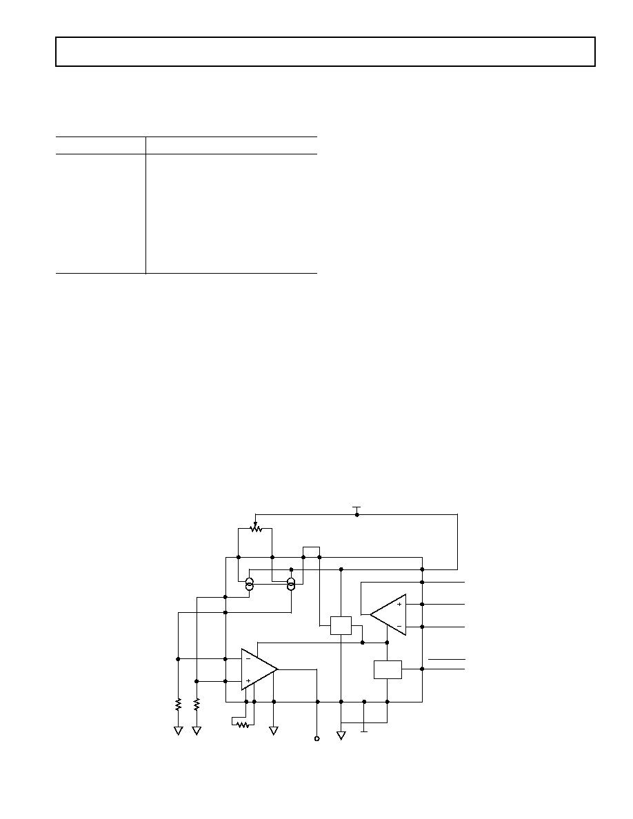
FUNCTIONAL DESCRIPTION
The ADT70 provides excitation and signal conditioning for
resistance-temperature devices (RTDs). It is ideally suited for
1 k
Platinum RTDs (PRTDs), which allow a much wider
range of temperature measurement than silicon-based sensors.
Using a low cost PRTD, the ADT70 can measure temperatures
in the range of 50
°
C to +500
°
C.
The two main components in the ADT70 are the adjustable
current sources and the instrumentation amplifier. The current
sources provide matching excitation currents to the PRTD and
to the Reference Resistor. The instrumentation amplifier com-
pares the voltage drop across both the PRTD and Reference
Resistor, and provides an amplified output signal voltage that is
proportional to temperature.
Besides the matching current sources and the instrumentation
amplifier, there is a general purpose op amp for any application
desired. The ADT70 comes with a +2.5 V reference on board.
RGA RGB
IN
IA
+IN
IA
INST
AMP
SHUT-
DOWN
GND
SENSE
OUT
IA
AGND
DGND
V
S
+IN
OA
IN
OA
OUT
OA
+V
S
2.5V
REF
I
OUTA
I
OUTB
MATCHED
CURRENT
SOURCES
NULLA
NULLB
BIAS 2.5V
REFOUT
ADT70
SHUTDOWN
Figure 26. Block Diagram
What is an RTD?
The measurable temperature range of the ADT70 heavily de-
pends on the characteristics of the resistance-temperature detec-
tor (RTD). Thus, it is important to choose the right RTD to
suit the actual application.
A basic physical property of any metal is that its electrical resis-
tivity changes with temperature. Some metals are known to have
a very predictable and repeatable change of resistance for a
given change in temperature. An RTD is fabricated from one of
these metals to a nominal ohmic value at a specified tempera-
ture. By measuring its resistance at some unknown temperature
and comparing this value to the resistor's nominal value, the
change in resistance is determined. Because the temperature vs.
resistance characteristics are also known, the change in tempera-
ture from the point initially specified can be calculated. This
makes the RTD a practical temperature sensor, which in its bare
form is a resistive element.
Several types of metal can be chosen for fabricating RTDs.
These include: Copper, balco (an iron-nickel alloy), nickel,
tungsten, iridium and platinum. Platinum is by far the most
popular material used, due to its nearly linear response to tem-
perature, wide temperature operating range and superior long-
term stability. The price of Platinum Resistance Temperature
Detectors (PRTDs) are becoming more competitive through the
wide use of thin-film-type resistive elements.
Temperature Coefficient of Resistance
The temperature coefficient (TC, also referred to as
) of an
RTD, describes the average resistance change per unit tempera-
ture from the ice point to the boiling point of water.
TCR
C
R
R
C
R
°
(
)
=
-
° ×
100
0
0
100
R
0
= Resistance of the sensor at 0
°
C
R
100
= Resistance of the sensor at +100
°
C
TCR = Thermal Coefficient of Resistance.
For example, a platinum thermometer measuring 100
at 0
°
C
and 138.5
at 100
°
C, has TCR 0.00385
/
/
°
C .
TCR
C
=
-
×
°
=
138 5
100
100
100
0 00385
.
.
The larger the TCR, the greater the change in resistance for a
given change in temperature. The most common use of TCR is
to distinguish between curves for platinum, which is available
with TCRs ranging from 0.00375 to 0.003927. The highest
TCR indicates the highest purity platinum and is mandated by
ITS-90 for standard platinum thermometers.
Basically, TCRs must be properly matched when replacing RTDs
or connecting them to instruments. There are no technical advan-
tages of one TCR over another in practical industrial applica-
tions. 0.00385 platinum is the most popular worldwide standard
and is available in both wire-wound and thin-film elements.
Understanding Error Source
The ADT70 uses an instrumentation amplifier that amplifies the
difference in voltage drop across the RTD and the reference resis-
tor, to output a voltage proportional to the measured temperature.
Thus, it is important to use a reference resistor that has stable resis-
tance over temperature. The accuracy of the reference resistor
should be determined by the end application.
The lead resistance of wires connecting to the RTD and the refer-
ence resistor can add inaccuracy to the ADT70. If the reference
resistor is located close to the part, while the RTD is located at a
remote location connected by wires, the lead-wires' resistance
TEMPERATURE C
0
50
SYSTEM RESPONSE TIME
s
0
10
25
25
50
75
100
125
20
30
40
50
V
OUT
OF IN AMP = 300mV
V
CC
= 5V SINGLE SUPPLY
= LOW TO HIGH
TURNING ON
V
SHUTDOWN
= HIGH TO LOW
TURNING OFF
V
SHUTDOWN
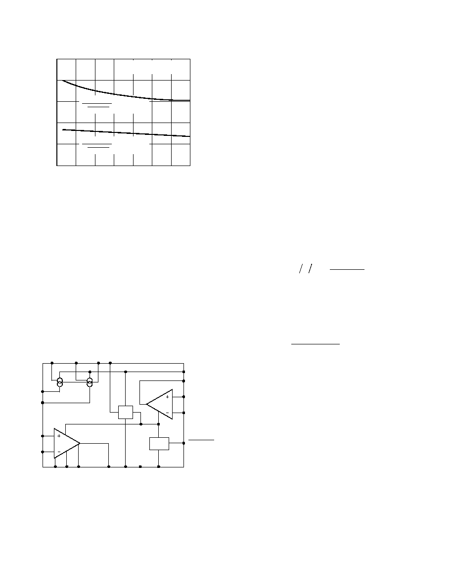
Figure 25. System Response Time from Shutdown vs.
Temperature
ADT70
REV. 0
9
would contribute to the difference in voltage drop between the
RTD and the reference resistor. Thus, an error in reading the ac-
tual temperature could occur.
Table I. Copper Wire Gauge Size to Resistance Table.
Lead-wire AWG
Ohms/foot at +25ºC
12
0.0016
14
0.0026
16
0.0041
18
0.0065
20
0.0103
22
0.0162
24
0.0257
26
0.0413
28
0.0651
30
0.1027
From Table I the amount of lead-wire resistance effect in the
circuit can be estimated. For example, connect 100 feet of
AWG 22 wire to a 100
Platinum RTD (PF element). The
lead-wire resistance will be: R = 100 ft 3 0.0162
/ft = 1.62
.
Thus the total resistance you have with the PRTD will be:
R
TOTAL
.
.
=
+
=
100
1 62
101 62
Since the 100
reference resistor is assumed to be relatively close
to the ADT70, the lead-wire resistance is negligible. This shows
1.62
of inaccuracy.
From the PRTD's data sheet, the PRTD's sensitivity rating
(
/
°
C) can be used with the lead-wire resistance to approximate
the accuracy error in temperature degree (
°
C). Following the ex-
ample above, the sensitivity of the 100
PRTD is 0.385
/
°
C
(taken from PRTD data sheet). Hence the approximate error is:
Error
C
C
=
° =
°
1 62
0 385
4 21
. / .
/
.
assuming the reference resistor is constant at 100
throughout
the temperature range.
As shown above, this is a significant inaccuracy, especially for ap-
plications where the PRTD would be hundreds of feet away from
the ADT70. To reduce lead-wire error it is recommended to use
a larger sensitivity RTD; 1 k
instead of 100
. Furthermore, in
the application circuit section, Figure 28 illustrates how to elimi-
nate such error by using the part's general purpose op amp.
Self-Heating Effect
Another contributor to measurement error is the self-heating ef-
fect on the RTD. As with any resistive element, power is dissi-
pated in an amount equal to the square of the excitation current
times the resistance of the element. The error contribution of the
heat generated by this power dissipation can easily be calculated.
For example, if the package thermal resistance is 50
°
C/W, the
RTD nominal resistance is 1 k
and the element is excited with a
1 mA current source, then the artificial increase in temperature
(
ºC) as a result of self-heating is:
° =
×
C
I R
PACKAGE
2
0
° =
( )
×
× °
C
mA
C W
1
1000
50
2
/
° =
°
C
C
0 05
.
where:
PACKAGE
= thermal resistance of package
R
0
= value of RTD resistance
APPLICATION INFORMATION
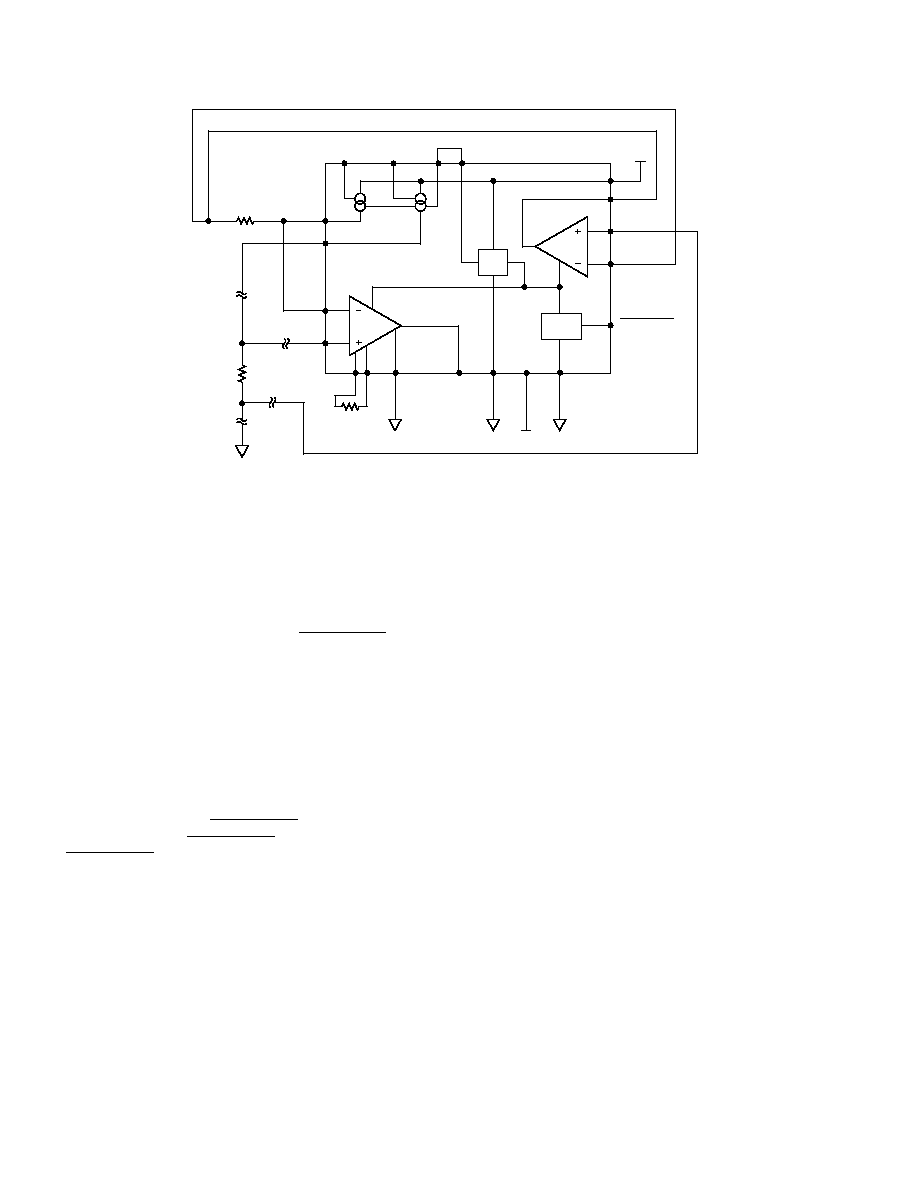
As shown in Figure 27, using a 1 k
PRTD, 1 k
reference
resistor, 49.9 k
resistor between RG
A
(Pin 11) and RG
B
(Pin
12), and shorting BIAS (Pin 4) with V
REFOUT
(Pin 3) together,
the output of OUT
IA
(Pin 14) will have a transfer function of
V
mV
R
OUT
PRTD RESISTANCE
REFERENCE RESISTANCE
=
×
(
)
1 299
.
/
-
RGA
RGB
+IN
IA
IN
IA
INST
AMP
SHUT-
DOWN
GND
SENSE
OUT
IA
AGND
DGND
V
S
SHUTDOWN
+IN
OA
IN
OA
OUT
OA
+V
S
2.5V
REF
I
OUTA
I
OUTB
MATCHED
CURRENT
SOURCES
NULLA
NULLB
BIAS
2.5V
REFOUT
ADT70
49.9k
V
OUT
@ 5mV/ C
INDEPENDENT
OP AMP
50k
+5V
1k
PRTD
1k
REF
RESISTOR
POTENTIOMETER
IS USED TO
ACHIEVE HIGHER
PRECISION OF
MATCHING
CURRENT.
1V <
V
S
< 5V
Figure 27. Basic Operational Diagram
ADT70
REV. 0
10
If PRTD has a tempco resistance of 0.00385
/
/
°
C or sensi-
tivity of 3.85
/
°
C, the system output voltage scaling factor will
be 5 mV/
°
C.
The gain of the instrumentation amplifier is normally at 1.30,
with a 49.9 k
gain resistor. It can be changed by changing the
gain resistor using the following equation.
Instrumentation Amp Gain
k
R
GAIN RESISTOR
.
.
=
1 30
49 9
In Figure 2 the ADT70 is powered by a dual power supply. In
order for the part to measure below 0
°
C, using a 1 k
PRTD,
V
S
has to be at least 1 V. V
S
can be grounded when the mea-
sured temperature is greater than 0
°
C using a 1 k
PRTD. GND
Sense (Pin 13), DGND (Pin 15), and AGND (Pin 2) are all con-
nected to ground. If desired, GND Sense could be connected to
whatever potential desired for an output offset of the instrumen-
tation amplifier. However, AGND and DGND must always be
connected to GND.
ADT70 will turn off if the
SHUTDOWN pin(GND) is low,
and will turn on when
SHUTDOWN pin becomes high (+V
S
).
If
SHUTDOWN is not used in the design, it should be con-
nected to +V
S
.
The undedicated op amp in the ADT70 can be used to transmit
measured signal to a remote location where noise might be intro-
duced into the signal as it travels in a noisy environment. It can
also be used as a general purpose amplifier in any application de-
sired. The op amp gain is set using standard feedback resistor
configurations.
Higher precision of matching the current sources can be
achieved by using a 50 k
potentiometer connected between
NULLA (Pin 5) and NULLB (Pin 6) with the center-tap of the
potentiometer connected to +V
S
(Pin 20). In Figure 27, the
ADT70's Bias Pin (Pin 4) is generally connected to the
V
REFOUT
(Pin 3), but it can be connected to an external voltage
reference if different output current is preferred.
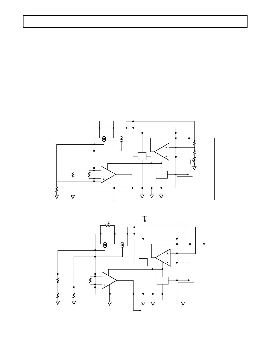
Eliminating Lead-Wire Resistance by Using 4-Wire
Configuration
In applications where the lead-wire resistance can significantly
contribute error to the measured temperature, implementing a
4-wire lead-resistance canceling circuit can dramatically mini-
mize the lead-wire resistance effect.
In Figure 28, I
OUTA
and I
OUTB
provides matching excitation to
the reference resistor and the PRTD respectively. The lead-re-
sistance from the current source to the PRTD or reference resis-
tor is not of concern because the instrumentation amplifier is
measuring the difference in potential directly on the PRTD
(Node A) and reference resistor (Node C). Since there is almost
no current going from Node A and Node C into the amplifier's
input, there is no lead-wire resistance error.
A potential source of temperature measurement errors is the
possibility of voltage differences between the ground side of the
reference resistor and the PRTD. Differences in lead-wire resis-
tance from ground to these two points, coupled with the 1 mA
excitation current, will lead directly to differential voltage errors
at the input of the instrumentation amplifier of the ADT70. By
connecting the ground side of the PRTD (Node B of Figure 28)
to the noninverting input of the op amp and connecting the
ground side of the reference resistor (Node D) to both the in-
verting input and the output of the op amp, the two points can
be forced to the same potential. It is not important that this po-
tential is exactly at ground since the instrumentation amplifier
rejects common-mode signals at the input. Note that all three
connections should be made as close as possible to the body of
the reference resistor and the PRTD to minimize error.
Single Supply Operation
When using the ADT70 in single supply applications a few
simple but important points need to be considered. The most
important issue is ensuring that the ADT70 is properly biased.
To bias the ADT70, first consider the 1 k
PRTD sensor. The
PRTD typically changes from 230
at 200
°
C to 4080
at
800
°
C
±
1
error. This impedance range results in an ADT70
output of 1 V to +4 V respectively, which is impossible to
RGA
RGB
+IN
IA
IN
IA
INST
AMP
SHUT-
DOWN
GND
SENSE
OUT
IA
DGND
V
S
SHUTDOWN
+IN
OA
IN
OA
OUT
OA
+V
S
2.5V
REF
I
OUTA
I
OUTB
MATCHED
CURRENT
SOURCES
NULLA
NULLB
BIAS
2.5V
REFOUT
ADT70
50k
1k
PRTD
NODE D
1k
REF
RESISTOR
NODE C
NODE B
NODE A
5V
AGND
5V
Figure 28. 4-Wire Lead-Wire Resistance Cancellation Circuit
ADT70
REV. 0
11
achieve in a single supply application where the negative rail is
ground or 0 V. Therefore, to achieve full scale operation the
output of ADT70 should be shifted by 1 V to allow for opera-
tion in the 0 V to 5 V region.
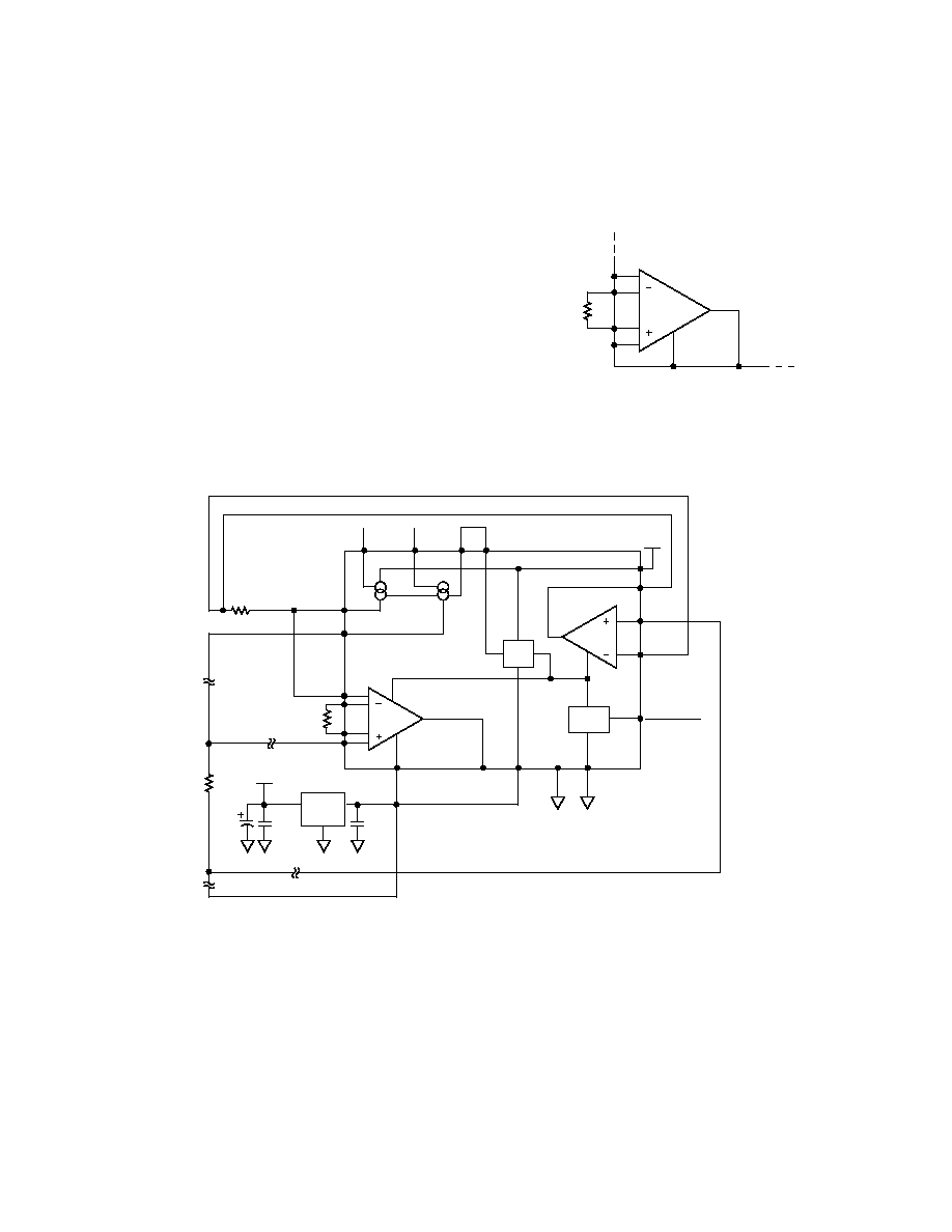
The most straightforward method to shift the output voltage
incorporates the use of the GND SENSE as shown in Figure 29.
To shift output voltage range apply a potential equal to the neces-
sary shift on the GND SENSE pin. For example, to shift the out-
put voltage, OUT
IA
, up to 1 V to GND SENSE, apply 1 V to
GND SENSE. When applying a potential to GND SENSE, care
should be taken to ensure that the voltage source is capable of driv-
ing 2 k
and does not introduce excessive noise. Figure 29 uses the
on-board 2.5 V voltage reference for a low noise source. This refer-
ence is then divided to 1 V and buffered by the on-board op amp
to drive GND SENSE at a low impedance. A small 500
potenti-
ometer can be used to calibrate the initial offset error to zero.
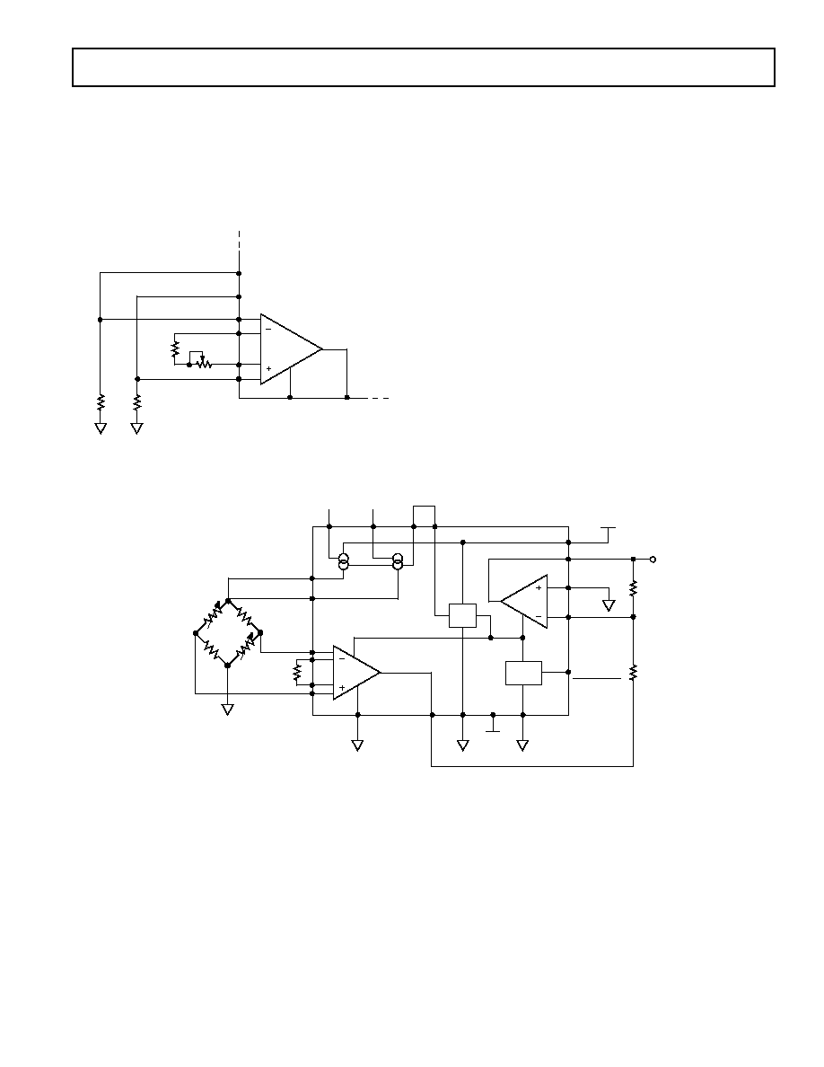
However, a voltage applied to GND SENSE is not the only
method to shift the voltage range. Placing a 768
resistor in the
PRTD sensor path also shifts the output voltage by 1 V. This
second method, as shown in Figure 30, is usually not recom-
mended for the following reasons; the input voltage range of the
op amps is limited to around 1 V from the negative and positive
rails and this could cause problems at high temperature, limiting
the upper range to 600
°
C; the physical location of this resistor
(if placed at a distance from the ADT70) may have an impact
on the noise performance. The method frees up the on-board op
amp for another function and achieves the lowest impedance
ground point for GND SENSE.
This brief section on ADT70 single supply operation has focused
on simple techniques to bias the ADT70 such that all output volt-
ages are within operational range. However, these techniques may
not be useful in all single supply applications. For example, in Fig-
ure 3 the additional on-board op amp is operating at near ground
potential which will create problems in a single supply application
+IN
IA
IN
IA
INST
AMP
SHUT-
DOWN
GND
SENSE
OUT
IA
DGND
SHUTDOWN
+IN
OA
IN
OA
OUT
OA
+V
S
2.5V
REF
I
OUTA
I
OUTB
MATCHED
CURRENT
SOURCES
NULLA
NULLB
BIAS
2.5V
REFOUT
1k
PRTD
SENSOR
RG
RG
49.9k
1k
REF
RESISTOR
TO CONTROLLER
15k
9.76k
500
POT
ADT70
Figure 29. A Single Supply Application with Shifted Ground Sense Pin
+IN
IA
IN
IA
INST
AMP
SHUT-
DOWN
GND
SENSE
DGND
SHUTDOWN
+IN
OA
IN
OA
OUT
OA
+V
S
2.5V
REF
I
OUTA
I
OUTB
MATCHED
CURRENT
SOURCES
NULLA
NULLB
BIAS
2.5V
REFOUT
1K
PRTD
RG
RG
49.9k
768
RESISTOR
TO CONTROLLER
1K
REF
RESISTOR
V
S
TO A/D CONVERTER
V
REF
+5V
ADT70
Figure 30. A Basic Single Supply Operational Diagram with Bias Resistor in Sensor Path
ADT70
REV. 0
12
because the input voltage range of the on-board op amp only ex-
tends to about 1 V above the negative rail. If the application re-
quires the inputs of either the on-board amp or instrumentation
amplifier to operate within 1 V of ground, it will be necessary to
generate a "pseudo-ground." Figure 31 illustrates a typical
ADT70 "pseudo-ground" application. The Analog Devices'
ADR290, a 2.048 V reference, is being used to generate the
"pseudo-ground." The ADR290 was selected for the following
reasons: low noise, ability to drive the required 5 mA in this
application, good temperature stability, which is usually impor-
tant in a PRTD application. However, one undesired effect of
introducing the pseudo-ground is the loss in voltage range at
high temperature. In our example, the PRTD will only operate
from 200
°
C to +400
°
C corresponding to an input voltage
range of 1 V to 4 V.
100 PRTD Application Circuit
A 1000
PRTD sensor scales by 3.85
s/
°
C, which is exactly
ten times the scale of the 100
PRTD sensor. The ADT70
has been designed to allow for 1000
or 100
PRTD sen-
sors. Only the gain setting resistor RG needs to be altered. For
a 100
PRTD 0.00385 sensor, change RG to 4.99 k
as illus-
trated in Figure 32. In single supply application, with a 100
PRTD sensor, a "pseudo-ground" will be necessary because the
inputs of the instrumentation amplifier will be within 1 V of the
negative rail. See the section on single supply applications for
more information.
+IN
IA
IN
IA
INST
AMP
RG
RG
4.99k
GND
SENSE
OUT
Figure 32. 100
0.00385 PRTD Application Showing
New Value for RG
+IN
IA
IN
IA
INST
AMP
SHUT-
DOWN
GND
SENSE
DGND
SHUTDOWN
+IN
OA
IN
OA
OUT
OA
+V
S
2.5V
REF
I
OUTA
I
OUTB
MATCHED
CURRENT
SOURCES
NULLA
NULLB
BIAS
2.5V
REFOUT
1k
PRTD
RG
RG
49.9k
V
S
OUT
IN
GND
ADR290
0.1 F
0.1 F
10 F
OUT
AGND
1k
REF
RESISTOR
NODE D
NODE C
+5V
+5V
ADT70
Figure 31. Single Supply Application with an ADR290 "Pseudo-Ground"
ADT70
REV. 0
13
American PRTD Application Circuit
The majority of PRTD sensors use a scale factor of 0.00385
/
/
°
C.
This type of sensor is known as the European PRTD and is the most
common PRTD sensor. However, there is also an American PRTD
sensor that uses a scale factor of 0.00392
/
/
°
C. Figure 33 illus-
trates the input section of the ADT70 configured for the Ameri-
can PRTD. The ideal value for RG is 50.98 k
when yielding a
5 mV/
°
C ADT70 output.
+IN
IA
IN
IA
INST
AMP
RG
RG
49.9k
2k
1k
REF
RESISTOR
1k
PRTD
I
OUTA
I
OUTB
NOTE: IDEAL VALUE
FOR RG
~
= 51k
GND
SENSE
OUT
Figure 33. Typical PRTD Application with American
0.003916
/
/
°
C Scale; 1 k
Scale
+IN
IA
IN
IA
INST
AMP
SHUT-
DOWN
DGND
SHUTDOWN
+IN
OA
IN
OA
OUT
OA
+V
S
2.5V
REF
I
OUTA
I
OUTB
MATCHED
CURRENT
SOURCES
NULLA
NULLB
BIAS
2.5V
REFOUT
RG
RG
+5V
R
R
R
R
COLUMBIA RESEARCH LAB
MODEL DT3617
STRAIN SENSOR
R = 1k
5V
ADT70
Figure 34. Typical Strain Sensor Application (Two Element Varying)
Strain Gauge Sensor Application Circuit
Figure 34 illustrates a typical strain gauge bridge circuit. The
versatility of the ADT70 allows the part to be used with most
bridge circuits that are within the 50 k
to 5 k
impedance
range. The sensor used in this circuit has two elements varying.
If a constant current is driven into the sensor, a linear V
OUT
is
obtained. In addition, the ADT70 will work with most bridge
circuits whether one-, two-, or all-element varying.
Securing Additional Current from the Current Sources
Some sensor applications need a higher excitation current to in-
crease sensor sensitivity. There are two methods to increase the
current from the on-board current sources of the ADT70. The
most flexible method involves changing the voltage at the BIAS
node. The equation for determining the BIAS potential vs. Out-
put current is 2.5 V for roughly 1 mA, or in other words, to
double the current output simply put 5 V into BIAS. The BIAS
node should be driven with a low-noise source, such as a refer-
ence, because output current is directly dependent on BIAS volt-
age. Directly tying BIAS to the positive supply rail may produce
too much current noise especially if the positive rail is not well
regulated. The second method involves tying the two ADT70
current outputs together which doubles the current. Of course,
this technique is most useful if, as illustrated in Figure 34, the ap-
plication requires only one current source.
ADT70
REV. 0
14
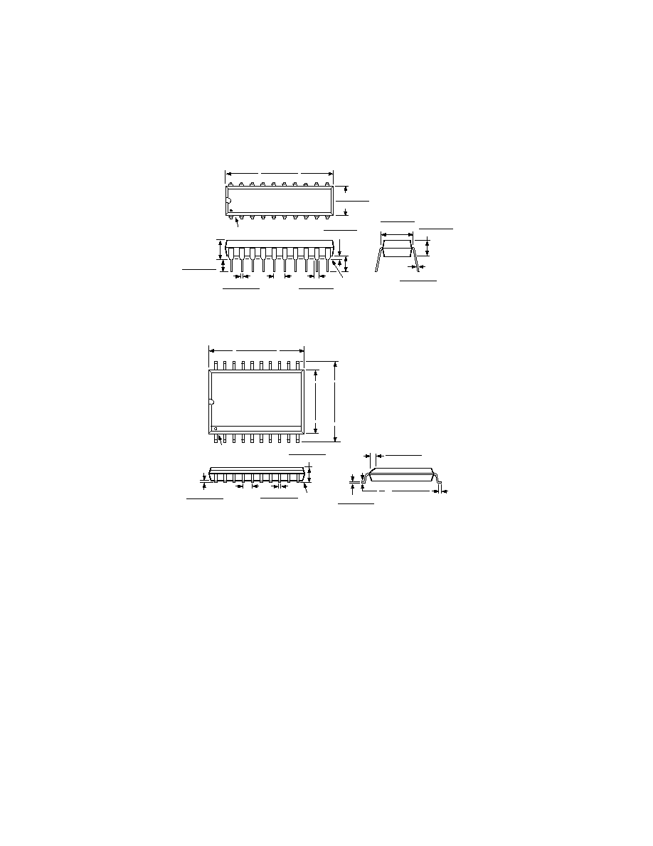
OUTLINE DIMENSIONS
Dimensions shown in inches and (mm).
20-Lead Plastic DIP
(P-Suffix)
20
1
10
11
1.060 (26.90)
0.925 (23.50)
0.280 (7.11)
0.240 (6.10)
PIN 1
SEATING
PLANE
0.022 (0.558)
0.014 (0.356)
0.060 (1.52)
0.015 (0.38)
0.210 (5.33)
MAX
0.130
(3.30)
MIN
0.070 (1.77)
0.045 (1.15)
0.100
(2.54)
BSC
0.160 (4.06)
0.115 (2.93)
0.325 (8.25)
0.300 (7.62)
0.015 (0.381)
0.008 (0.204)
0.195 (4.95)
0.115 (2.93)
20-Lead SOIC
(S-Suffix)
SEATING
PLANE
0.0118 (0.30)
0.0040 (0.10)
0.0192 (0.49)
0.0138 (0.35)
0.1043 (2.65)
0.0926 (2.35)
0.0500
(1.27)
BSC
0.0125 (0.32)
0.0091 (0.23)
0.0500 (1.27)
0.0157 (0.40)
8
°
0
°
0.0291 (0.74)
0.0098 (0.25)
x 45
°
20
11
10
1
0.5118 (13.00)
0.4961 (12.60)
0.4193 (10.65)
0.3937 (10.00)
0.2992 (7.60)
0.2914 (7.40)
PIN 1
C339587/98
PRINTED IN U.S.A.