Äîêóìåíòàöèÿ è îïèñàíèÿ www.docs.chipfind.ru
Preliminary Technical Data
TigerSHARC and the TigerSHARC logo are registered trademarks of Analog Devices, Inc.
TigerSHARC
®
Embedded Processor
ADSP-TS201S
Rev. PrH
Information furnished by Analog Devices is believed to be accurate and reliable.
However, no responsibility is assumed by Analog Devices for its use, nor for any
infringements of patents or other rights of third parties that may result from its use.
Specifications subject to change without notice. No license is granted by implication
or otherwise under any patent or patent rights of Analog Devices. Trademarks and
registered trademarks are the property of their respective owners.
One Technology Way, P.O.Box 9106, Norwood, MA 02062-9106 U.S.A.
Tel:781/329-4700
www.analog.com
Fax:781/326-8703
© 2003 Analog Devices, Inc. All rights reserved.
KEY FEATURES
Up to 600 MHz, 1.67 ns Instruction Cycle Rate
24M Bits of Internal--On-Chip--DRAM Memory
25×25 mm (576-Ball) Thermally Enhanced Ball Grid Array
Package
Dual Computation Blocks--Each Containing an ALU, a Multi-
plier, a Shifter, a Register File, and a Communications Logic
Unit (CLU)
Dual Integer ALUs, providing Data Addressing and Pointer
Manipulation
Integrated I/O Includes 14 Channel DMA Controller, External
Port, Four Link Ports, SDRAM Controller, Programmable
Flag Pins, Two Timers, and Timer Expired Pin for System
Integration
1149.1 IEEE Compliant JTAG Test Access Port for On-Chip
Emulation
On-Chip Arbitration for Glueless Multiprocessing
KEY BENEFITS
Provides High-Performance Static Superscalar DSP Opera-
tions, Optimized for Telecommunications Infrastructure
and Other Large, Demanding Multiprocessor DSP
Applications
Performs Exceptionally Well on DSP Algorithm and I/O
Benchmarks (See Benchmarks in
Table 1
)
Supports Low-Overhead DMA Transfers Between Internal
Memory, External Memory, Memory-Mapped Peripherals,
Link Ports, Host Processors, and Other (Multiprocessor)
DSPs
Eases DSP Programming Through Extremely Flexible Instruc-
tion Set and High-Level-Language Friendly DSP
Architecture
Enables Scalable Multiprocessing Systems With Low Commu-
nications Overhead
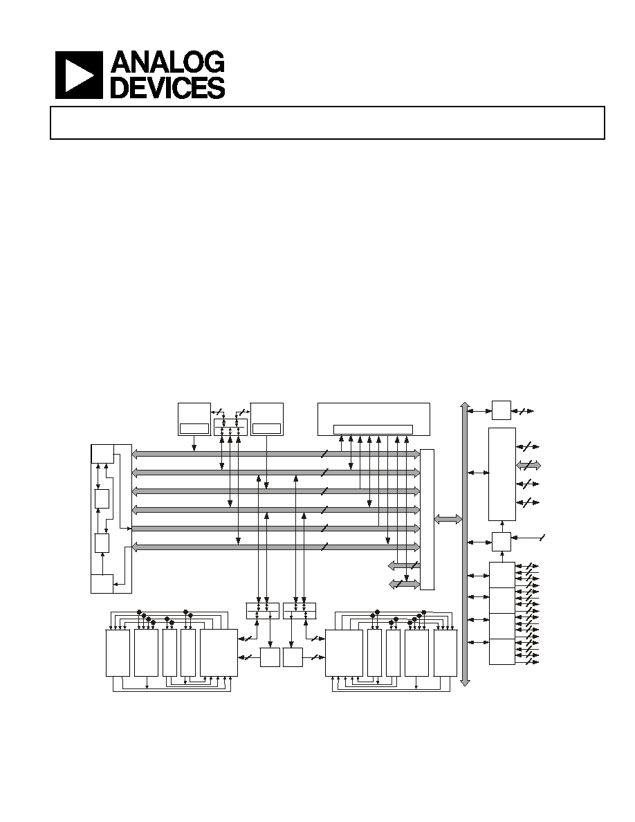
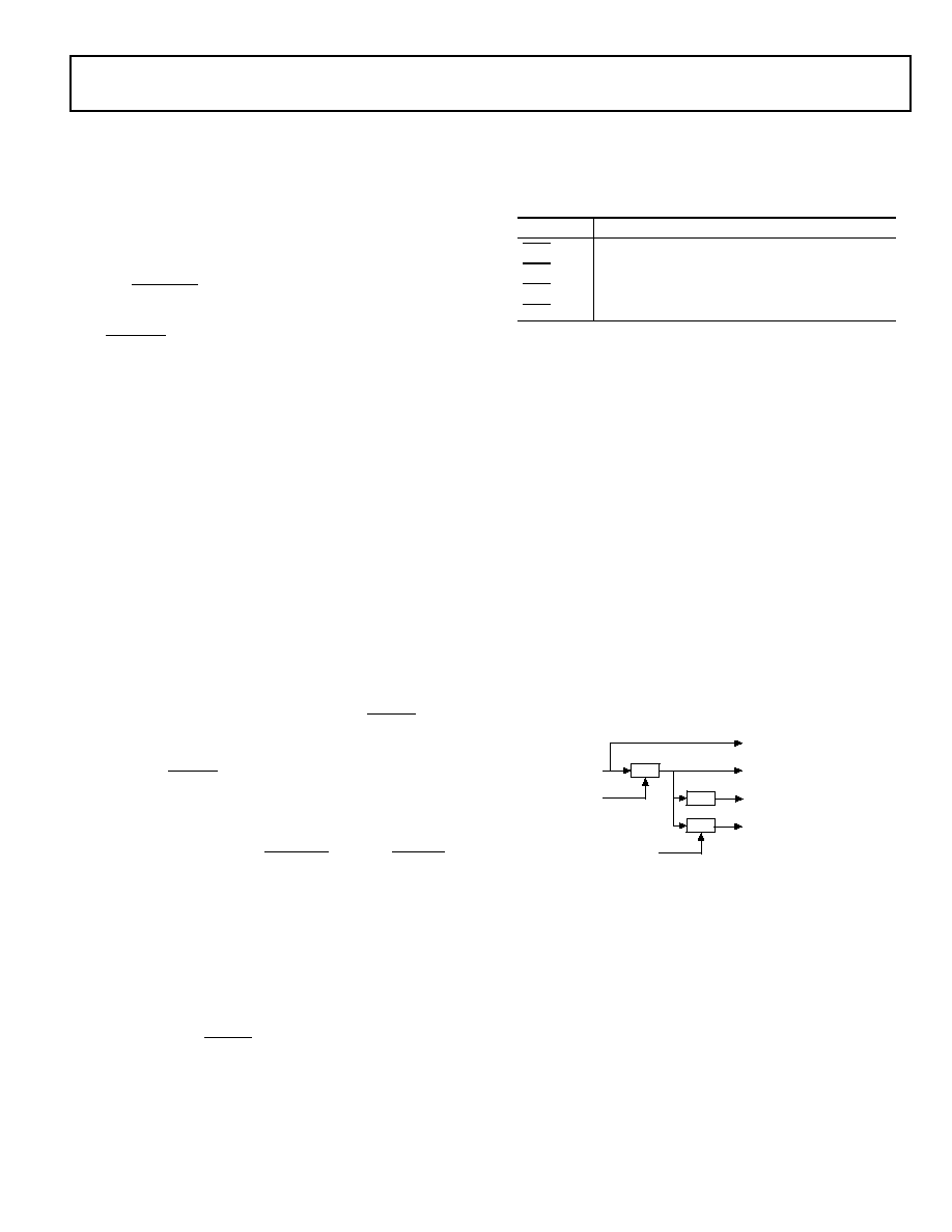
Figure 1. Functional block diagram
T
L0
8
4
8
4
8
4
8
4
8
4
8
4
8
4
8
4
IN
OUT
HOST
MULTI
PROC
C-BUS
ARB
DATA
64
LINK PORTS
JTAG PORT
EXTERNAL
PORT
ADDR
32
6
SOC BUS
DMA
JTAG
SDRAM
CTRL
EXT DMA
REQ
J-BUS DATA
IAB
PC
BTB
ADDR
FETCH
PROGRAM
SEQUENCER
COMPUTATIONAL BLOCKS
J-BUS ADDR
K-BUS DATA
K-BUS ADDR
I-BUS DATA
I-BUS ADDR
S-BUS DATA
S-BUS ADDR
INTEGER
K ALU
INTEGER
J ALU
32
32
32X32
32X32
DATA ADDRESS GENERATION
X
REGISTER
FILE
32x32
M
U
L
T
I
P
L
I
E
R
A
L
U
S
H
I
F
T
E
R
C
L
U
DAB
128
128
DAB
128
128
MEMORY BLOCKS
A
D
24M BITS INTERNAL MEMORY
4xCROSSBAR CONNECT
(PAGE CACHE)
A
D
A
D
A
D
S
O
C
I
N
T
E
R
F
A
C
E
Y
REGISTER
FILE
32x32
M
U
L
T
I
P
L
I
E
R
A
L
U
S
H
I
F
T
E
R
C
L
U
L1
IN
OUT
L2
IN
OUT
L3
IN
OUT
CTRL
8
CTRL
10
32
128
32
128
32
128
32
128
4

Rev. PrH
|
Page 2 of 40
|
December 2003
ADSP-TS201S
Preliminary Technical Data
TABLE OF CONTENTS
General Description ................................................. 3
Dual Compute Blocks ............................................ 4
Data Alignment Buffer (DAB) .................................. 4
Dual Integer ALU (IALU) ....................................... 4
Program Sequencer ............................................... 5
Interrupt Controller ........................................... 5
Flexible Instruction Set ........................................ 5
DSP Memory ....................................................... 5
External Port
(Off-Chip Memory/Peripherals Interface) ................ 6
Host Interface ................................................... 6
Multiprocessor Interface ...................................... 7
SDRAM Controller ............................................ 7
EPROM Interface .............................................. 7
DMA Controller ................................................... 7
Link Ports (LVDS) ................................................ 8
Timer and General-Purpose I/O ............................... 9
Reset and Booting ................................................. 9
Clock Domains .................................................... 9
Power Domains .................................................... 9
Filtering Reference Voltage and Clocks ...................... 9
Development Tools ............................................. 10
Designing an Emulator-Compatible DSP Board (Target) 11
Additional Information ........................................ 11
Pin Function Descriptions ........................................ 12
Strap Pin Function Descriptions ................................ 19
ADSP-TS201S--Specifications ................................... 21
Recommended Operating Conditions ...................... 21
Electrical Characteristics ....................................... 21
Absolute Maximum Ratings ................................... 22
ESD Sensitivity ................................................... 22
Timing Specifications ........................................... 23
General AC Timing .......................................... 23
Link Port Low-Voltage, Differential-Signal (LVDS)
Electrical Characteristics and Timing ................. 27
Link Port--Data Out Timing ........................... 28
Link Port--Data In Timing .............................. 31
Output Drive Currents ......................................... 32
Test Conditions .................................................. 33
Output Disable Time ......................................... 33
Output Enable Time ......................................... 34
Capacitive Loading ........................................... 34
Environmental Conditions .................................... 36
Thermal Characteristics ..................................... 36
576-Ball BGA_ED Pin Configurations ......................... 36
Outline Dimensions ................................................ 40
Ordering Guide ..................................................... 40
REVISION HISTORY
Revision PrH:
· Applies corrections and additional information (includ-
ing information on 600 MHz parts) to
VREF Filtering
Scheme (page 10)
,
SCLK_VREF Filtering Scheme
(page 10)
,
Drive Strength/Output Impedance Selection
(page 19)
,
Recommended Operating Conditions
(page 22)
,
Electrical Characteristics (page 22)
,
Reference
Clocks (page 24)
,
Power-Up Reset Timing (page 25)
,
AC
Signal Specifications (page 26)
,
Link Port--Data Out
Timing (page 29)
,
Link Port--Data In Timing (page 32)
,
and
Ordering Guide (page 42)
.
· Provides unused pin termination data in
Pin Function
Descriptions (page 13)
.
· Changes pins R2 and R3 to NC in
576-Ball (25 mm × 25
mm) BGA_ED Pin Assignments (page 38)
.
ADSP-TS201S
Preliminary Technical Data
Rev. PrH
|
Page 3 of 40
|
December 2003
GENERAL DESCRIPTION
The ADSP-TS201S TigerSHARC processor is an ultra-high per-
formance, static superscalar processor optimized for large signal
processing tasks and communications infrastructure. The DSP
combines very wide memory widths with dual computation
blocks--supporting 32- and 40-bit floating-point and support-
ing 8-, 16-, 32-, and 64-bit fixed-point processing--to set a new
standard of performance for digital signal processors. The
TigerSHARC static superscalar architecture lets the DSP exe-
cute up to four instructions each cycle, performing twenty-four
16-bit fixed-point operations or six floating-point operations.
Four independent 128-bit wide internal data buses, each con-
necting to the six 4M bit memory banks, enable quad-word
data, instruction, and I/O accesses and provide 33.6G bytes per
second of internal memory bandwidth. Operating at 600 MHz,
the ADSP-TS201S processor's core has a 1.67 ns instruction
cycle time. Using its Single-Instruction, Multiple-Data (SIMD)
features, the ADSP-TS201S processor can perform 4.8 billion
40-bit MACs or 1.2 billion 80-bit MACs per second.
Table 1
shows the DSP's performance benchmarks.
The ADSP-TS201S processor is code-compatible with the other
TigerSHARC processors.
The Functional Block Diagram
on page 1
shows the ADSP-
TS201S processor's architectural blocks. These blocks include:
· Dual compute blocks, each consisting of an ALU, multi-
plier, 64-bit shifter, 128-bit CLU, and 32-word register file
and associated Data Alignment Buffers (DABs)
· Dual integer ALUs (IALUs), each with its own 31-word
register file for data addressing and a status register
· A program sequencer with Instruction Alignment Buffer
(IAB) and Branch Target Buffer (BTB)
· An interrupt controller that supports hardware and soft-
ware interrupts, supports level- or edge-triggers, and
supports prioritized, nested interrupts
· Four 128-bit internal data buses, each connecting to the six
4M bit memory banks
· On-chip DRAM (24M bit)
· An external port that provides the interface to host proces-
sors, multiprocessing space (DSPs), off-chip memory-
mapped peripherals, and external SRAM and SDRAM
· A 14 channel DMA controller
· Four full-duplex LVDS link ports
· Two 64-bit interval timers and timer expired pin
· A 1149.1 IEEE compliant JTAG test access port for on-chip
emulation
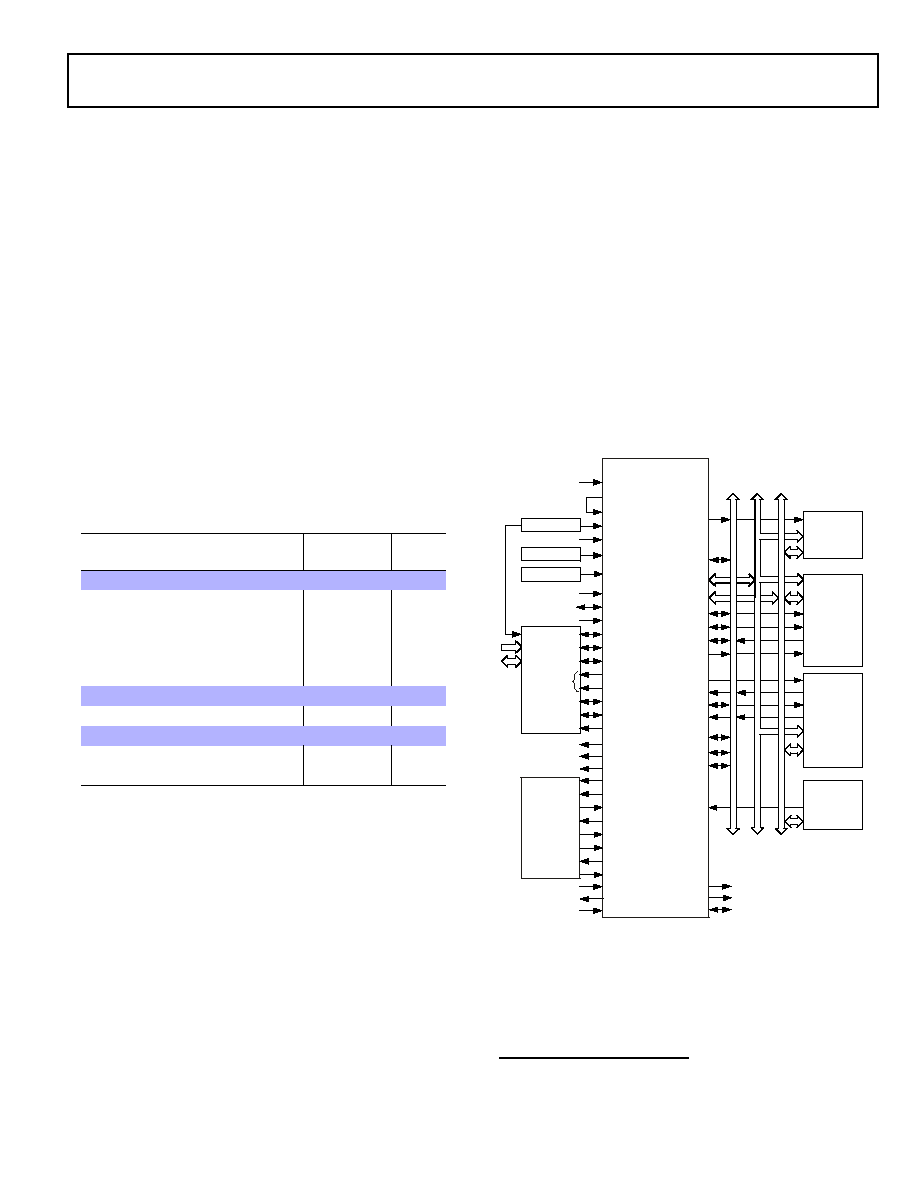
Figure 2 on page 3
shows a typical single-processor system with
external SRAM and SDRAM.
Figure 3 on page 6
shows a typical
multiprocessor system.
The TigerSHARC DSP uses a Static Superscalar
*
architecture.
This architecture is superscalar in that the ADSP-TS201S pro-
cessor's core can execute simultaneously from one to four 32-bit
instructions encoded in a Very Large Instruction Word (VLIW)
instruction line using the DSP's dual compute blocks. Because
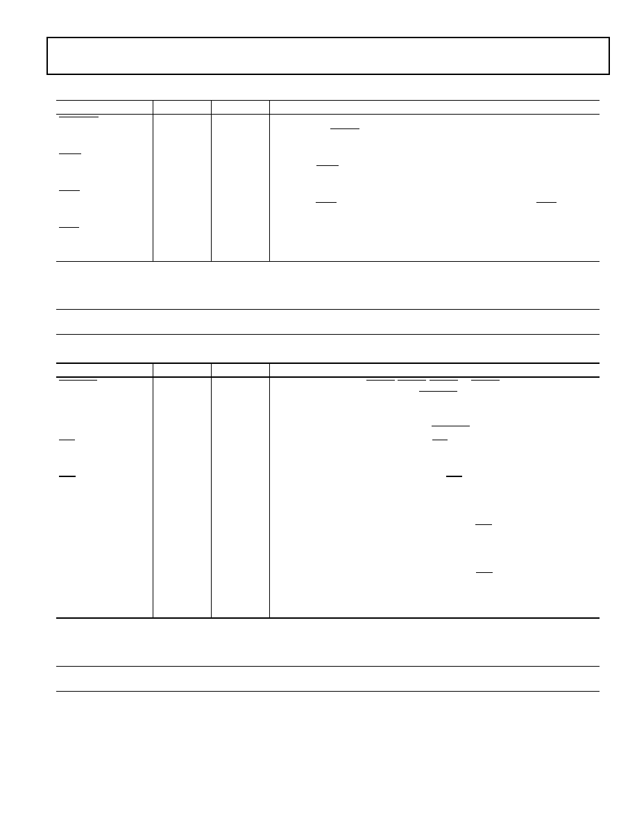
Table 1. General Purpose Algorithm Benchmarks
at 600 MHz
Benchmark
Speed
Clock
Cycles
32-bit Algorithm, 1.2 billion MACs/s peak performance
1K Point Complex FFT
1
(Radix2)
15.7 µs
9419
64K Point Complex FFT
1
(Radix2)
2.33 ms
1397544
FIR Filter (per real tap)
0.83 ns
0.5
[8 × 8][8 × 8] Matrix Multiply (Complex,
Floating-point)
2.3 µs
1399
16-bit Algorithm, 4.8 billion MACs/s peak performance
256 Point Complex FFT
1
(Radix 2)
1
Cache preloaded
1.5 µs
928
I/O DMA Transfer Rate
External port
1G bytes/s
n/a
Link ports (each)
1G bytes/s
n/a
Figure 2. ADSP-TS201S Single-Processor System With External SDRAM
*
Static SuperscalarTM is a trademark of Analog Devices, Inc.
BOFF
CONTROLIMP10
DMAR30
HBG
HBR
DMA DEVICE
(OPTIONAL)
DATA
MSH
FLAG30
ID20
IOEN
RAS
CAS
LDQM
HDQM
SDWE
SDCKE
SDA10
IRQ30
SCLK
SCLKRAT20
SCLK_V
REF
V
REF
TMR0E
BM
MSSD30
BUSLOCK
SDRAM
MEMORY
(OPTIONAL)
CS
RAS
CAS
DQM
WE
CKE
A10
ADDR
DATA
CLK
POR_IN
JTAG
ADSP-TS201S
BMS
CLOCK
LINK
DEVICES
(4 MAX)
(OPTIONAL)
BOOT
EPROM
(OPTIONAL)
ADDR
MEMORY
(OPTIONAL)
OE
DATA
ADDR
DATA
HOST
PROCESSOR
INTERFACE
(OPTIONAL)
ACK
BR70
CPA
MS10
DATA630
DATA
ADDR
CS
ACK
WE
ADDR310
D
A
T
A
C
O
N
T
R
O
L
A
D
D
R
E
S
S
BRST
REFERENCE
RD
WRH/WRL
DPA
DS20
CS
LxCLKINP/N
LxACKO
LxDATI30P/N
LxBCMPI
LxBCMPO
LxDATO30P/N
LxCLKOUTP/N
LxACKI
IORD
IOWR
RST_OUT
RST_IN
REFERENCE

Rev. PrH
|
Page 4 of 40
|
December 2003
ADSP-TS201S
Preliminary Technical Data
the DSP does not perform instruction re-ordering at runtime--
the programmer selects which operations will execute in parallel
prior to runtime--the order of instructions is static.
With few exceptions, an instruction line, whether it contains
one, two, three, or four 32-bit instructions, executes with a
throughput of one cycle in a ten-deep processor pipeline.
For optimal DSP program execution, programmers must follow
the DSP's set of instruction parallelism rules when encoding an
instruction line. In general, the selection of instructions that the
DSP can execute in parallel each cycle depends on the instruc-
tion line resources each instruction requires and on the source
and destination registers used in the instructions. The program-
mer has direct control of three core components--the IALUs,
the compute blocks, and the program sequencer.
The ADSP-TS201S processor, in most cases, has a two-cycle
execution pipeline that is fully interlocked, so--whenever a
computation result is unavailable for another operation depen-
dent on it--the DSP automatically inserts one or more stall
cycles as needed. Efficient programming with dependency-free
instructions can eliminate most computational and memory
transfer data dependencies.
In addition, the ADSP-TS201S processor supports SIMD opera-
tions two ways--SIMD compute blocks and SIMD
computations. The programmer can load both compute blocks
with the same data (broadcast distribution) or different data
(merged distribution).
DUAL COMPUTE BLOCKS
The ADSP-TS201S processor has compute blocks that can exe-
cute computations either independently or together as a Single-
Instruction, Multiple-Data (SIMD) engine. The DSP can issue
up to two compute instructions per compute block each cycle,
instructing the ALU, multiplier, shifter, or CLU to perform
independent, simultaneous operations. Each compute block can
execute eight 8-bit, four 16-bit, two 32-bit, or one 64-bit SIMD
computations in parallel with the operation in the other block.
The compute blocks are referred to as X and Y in assembly syn-
tax, and each block contains four computational units--an
ALU, a multiplier, a 64-bit shifter, a 128-bit CLU--and a 32-
word register file.
· Register File--Each Compute Block has a multiported 32-
word, fully orthogonal register file used for transferring
data between the computation units and data buses and for
storing intermediate results. Instructions can access the
registers in the register file individually (word-aligned), in
sets of two (dual-aligned), or in sets of four (quad-aligned).
· ALU--The ALU performs a standard set of arithmetic
operations in both fixed- and floating-point formats. It also
performs logic operations.
· Multiplier--The multiplier performs both fixed- and float-
ing-point multiplication and fixed-point multiply and
accumulate.
· Shifter--The 64-bit shifter performs logical and arithmetic
shifts, bit and bitstream manipulation, and field deposit
and extraction operations.
· Communications Logic Unit (CLU)--This is a 128-bit unit
provides Trellis Decoding (for example, Viterbi and Turbo
decoders) and executes complex correlations for CDMA
communication applications (for example chip-rate and
symbol-rate functions).
Using these features, the compute blocks can:
· Provide 8 MACs per cycle peak and 7.1 MACs per cycle
sustained 16-bit performance and provide 2 MACs per
cycle peak and 1.8 MACs per cycle sustained 32-bit perfor-
mance (based on FIR)
· Execute six single-precision floating-point or execute
twenty-four 16-bit fixed-point operations per cycle, pro-
viding 3 GFLOPS or 12.0 GOPS performance
· Perform two complex 16-bit MACs per cycle
· Execute eight Trellis butterflies in one cycle
DATA ALIGNMENT BUFFER (DAB)
The DAB is a quad-word FIFO that enables loading of quad-
word data from nonaligned addresses. Normally, load instruc-
tions must be aligned to their data size so that quad words are
loaded from a quad-aligned address. Using the DAB signifi-
cantly improves the efficiency of some applications, such as FIR
filters.
DUAL INTEGER ALU (IALU)
The ADSP-TS201S processor has two IALUs that provide pow-
erful address generation capabilities and perform many general-
purpose integer operations. The IALUs are referred to as J and
K in assembly syntax and have the following features:
· Provides memory addresses for data and update pointers
· Supports circular buffering and bit-reverse addressing
· Performs general-purpose integer operations, increasing
programming flexibility
· Includes a 31-word register file for each IALU
As address generators, the IALUs perform immediate or indi-
rect (pre- and post-modify) addressing. They perform modulus
and bit-reverse operations with no constraints placed on mem-
ory addresses for the modulus data buffer placement. Each
IALU can specify either a single-, dual-, or quad-word access
from memory.
The IALUs have hardware support for circular buffers, bit
reverse, and zero-overhead looping. Circular buffers facilitate
efficient programming of delay lines and other data structures
required in digital signal processing, and they are commonly
used in digital filters and Fourier transforms. Each IALU pro-
vides registers for four circular buffers, so applications can set
up a total of eight circular buffers. The IALUs handle address
pointer wraparound automatically, reducing overhead, increas-
ing performance, and simplifying implementation. Circular
buffers can start and end at any memory location.

ADSP-TS201S
Preliminary Technical Data
Rev. PrH
|
Page 5 of 40
|
December 2003
Because the IALU's computational pipeline is one cycle deep, in
most cases integer results are available in the next cycle. Hard-
ware (register dependency check) causes a stall if a result is
unavailable in a given cycle.
PROGRAM SEQUENCER
The ADSP-TS201S processor's program sequencer supports the
following:
· A fully interruptible programming model with flexible pro-
gramming in assembly and C/C++ languages; handles
hardware interrupts with high throughput and no aborted
instruction cycles
· A ten-cycle instruction pipeline--four-cycle fetch pipe and
six-cycle execution pipe--computation results available
two cycles after operands are available
· Supply of instruction fetch memory addresses; the
sequencer's Instruction Alignment Buffer (IAB) caches up
to five fetched instruction lines waiting to execute; the pro-
gram sequencer extracts an instruction line from the IAB
and distributes it to the appropriate core component for
execution
· Management of program structures and program flow
determined according to JUMP, CALL, RTI, RTS instruc-
tions, loop structures, conditions, interrupts, and software
exceptions
· Branch prediction and a 128-entry branch target buffer
(BTB) to reduce branch delays for efficient execution of
conditional and unconditional branch instructions and
zero-overhead looping; correctly predicted branches that
are taken occur with zero overhead cycles, overcoming the
five-to-nine stage branch penalty
· Compact code without the requirement to align code in
memory; the IAB handles alignment
Interrupt Controller
The DSP supports nested and nonnested interrupts. Each inter-
rupt type has a register in the interrupt vector table. Also, each
has a bit in both the interrupt latch register and the interrupt
mask register. All interrupts are fixed as either level-sensitive or
edge-sensitive, except the IRQ30 hardware interrupts, which
are programmable.
The DSP distinguishes between hardware interrupts and soft-
ware exceptions, handling them differently. When a software
exception occurs, the DSP aborts all other instructions in the
instruction pipe. When a hardware interrupt occurs, the DSP
continues to execute instructions already in the instruction pipe.
Flexible Instruction Set
The 128-bit instruction line, which can contain up to four 32-bit
instructions, accommodates a variety of parallel operations for
concise programming. For example, one instruction line can
direct the DSP to conditionally execute a multiply, an add, and a
subtract in both computation blocks while it also branches to
another location in the program. Some key features of the
instruction set include:
· CLU instructions for communications infrastructure to
govern Trellis Decoding (for example, Viterbi and Turbo
decoders) and Despreading via complex correlations
· Algebraic assembly language syntax
· Direct support for all DSP, imaging, and video arithmetic
types
· Eliminates toggling DSP hardware modes because modes
are supported as options (for example, rounding, satura-
tion, and others) within instructions
· Branch prediction encoded in instruction; enables zero-
overhead loops
· Parallelism encoded in instruction line
· Conditional execution optional for all instructions
· User defined partitioning between program and data
memory
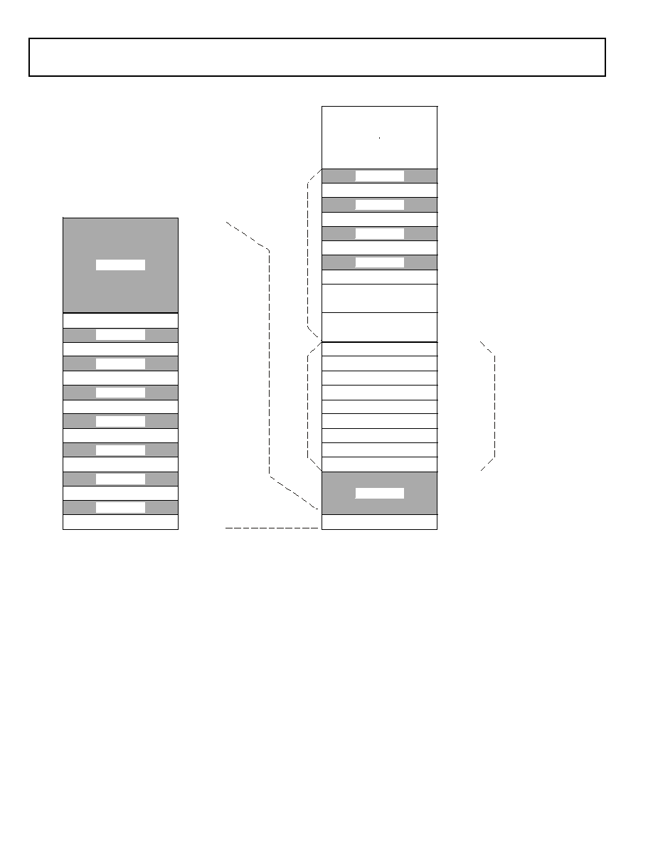
DSP MEMORY
The DSP's internal and external memory is organized into a
unified memory map, which defines the location (address) of all
elements in the system, as shown in
Figure 3
.
The memory map is divided into four memory areas--host
space, external memory, multiprocessor space, and internal
memory--and each memory space, except host memory, is sub-
divided into smaller memory spaces.
The ADSP-TS201S processor internal memory has 24M bits of
on-chip DRAM memory, divided into six blocks of 4M bits
(128K words × 32 bits). Each block--M0, M2, M4, M6, M8, and
M10--can store program, data, or both, so applications can
configure memory to suit specific needs. Placing program
instructions and data in different memory blocks, however,
enables the DSP to access data while performing an instruction
fetch. Each memory segment contains a 128K bit cache to
enable single cycle accesses to internal DRAM.
The six internal memory blocks connect to the four 128-bit wide
internal buses through a crossbar connection, enabling the DSP
to perform four memory transfers in the same cycle. The DSP's
internal bus architecture provides a total memory bandwidth of
33.6G bytes per second, enabling the core and I/O to access
eight 32-bit data words and four 32-bit instructions each cycle.
The DSP's flexible memory structure enables:
· DSP core and I/O accesses to different memory blocks in
the same cycle
· DSP core access to three memory blocks in parallel--one
instruction and two data accesses
· Programmable partitioning of program and data memory
· Program access of all memory as 32-, 64-, or 128-bit
words--16-bit words with the DAB
Rev. PrH
|
Page 6 of 40
|
December 2003
ADSP-TS201S
Preliminary Technical Data
EXTERNAL PORT
(OFF-CHIP MEMORY/PERIPHERALS INTERFACE)
The ADSP-TS201S processor's external port provides the DSP's
interface to off-chip memory and peripherals. The 4G word
address space is included in the DSP's unified address space.
The separate on-chip buses--four 128-bit data buses and four
32-bit address buses--are multiplexed at the SOC interface and
transferred to the external port over the SOC bus to create an
external system bus transaction. The external system bus pro-
vides a single 64-bit data bus and a single 32-bit address bus.
The external port supports data transfer rates of 1G bytes per
second over the external bus.
The external bus can be configured for 32- or 64-bit, little-
endian operations. When the system bus is configured for 64-bit
operations, the lower 32 bits of the external data bus connect to
even addresses, and the upper 32 bits connect to odd addresses.
The external port supports pipelined, slow, and SDRAM proto-
cols. Addressing of external memory devices and memory-
mapped peripherals is facilitated by on-chip decoding of high-
order address lines to generate memory bank select signals.
The ADSP-TS201S processor provides programmable memory,
pipeline depth, and idle cycle for synchronous accesses, and
external acknowledge controls to support interfacing to pipe-
lined or slow devices, host processors, and other memory-
mapped peripherals with variable access, hold, and disable time
requirements.
Host Interface
The ADSP-TS201S processor provides an easy and configurable
interface between its external bus and host processors through
the external port. To accommodate a variety of host processors,
Figure 3. ADSP-TS201S Memory Map
RESERVED
RESERVED
INTERNAL REGISTERS (UREG S)
INTERNAL MEMO RY BLOCK 4
INTERNAL MEMORY BLOCK 2
INTERNAL MEMORY BLOCK 0
0x03FFFFFF
0X001E0000
0x001E03FF
0x000DFFFF
0x000C0000
0x0009FFFF
0x00080000
0x0005FFFF
0x00040000
0x0001FFFF
0x00000000
INTERNAL SPACE
PROCESSO R ID 7
PROCESSO R ID 6
PROCESSO R ID 5
PROCESSO R ID 4
PROCESSO R ID 3
PROCESSO R ID 2
PROCESSO R ID 1
PROCESSO R ID 0
BROADCAST
HOST (
MSH
)
BANK 1 (
MS1
)
BANK 0 (
MS0
)
MSSD BANK 0 (
MSSD0
)
INTERNAL MEMORY
0x50000000
0x40000000
0x38000000
0x30000000
0x2C000000
0x28000000
0x24000000
0x20000000
0x1C000000
0x18000000
0x14000000
0x10000000
0X0C000000
0x03FFFFFF
0x00000000
GLOBAL SPACE
0xFFFFFFFF
M
U
L
T
I
P
R
O
C
E
S
S
O
R
M
E
M
O
R
Y
S
P
A
C
E
E
X
T
E
R
N
A
L
M
E
M
O
R
Y
S
P
A
C
E
EACH IS A COPY
OF INTERNAL SPACE
RESERVED
INTERNAL MEMO RY BLOCK 6
INTERNAL MEMO RY BLOCK 8
0x0011FFFF
0x00100000
INTERNAL MEMO RY BL OCK 10
0x0015FFFF
0x00140000
RESERVED
RESERVED
RESERVED
RESERVED
RESERVED
RESERVED
SOC REGISTERS (UREGS)
0X001F0000
0x001F03FF
MSSD BANK 1 (
MSSD1
)
MSSD BANK 2 (
MSSD2
)
MSSD BANK 3 (
MSSD3
)
0x60000000
0x70000000
0x80000000
RESERVED
RESERVED
RESERVED
RESERVED
0x54000000
0x44000000
0x64000000
0x74000000

ADSP-TS201S
Preliminary Technical Data
Rev. PrH
|
Page 7 of 40
|
December 2003
the host interface supports pipelined or slow protocols for
ADSP-TS201S processor accesses of the host as slave or pipe-
lined for host accesses of the ADSP-TS201S processor as slave.
Each protocol has programmable transmission parameters,
such as idle cycles, pipe depth, and internal wait cycles.
The host interface supports burst transactions initiated by a host
processor. After the host issues the starting address of the burst
and asserts the BRST signal, the DSP increments the address
internally while the host continues to assert BRST.
The host interface provides a deadlock recovery mechanism that
enables a host to recover from deadlock situations involving the
DSP. The BOFF signal provides the deadlock recovery mecha-
nism. When the host asserts BOFF, the DSP backs off the
current transaction and asserts HBG and relinquishes the exter-
nal bus.
The host can directly read or write the internal memory of the
ADSP-TS201S processor, and it can access most of the DSP reg-
isters, including DMA control (TCB) registers. Vector
interrupts support efficient execution of host commands.
Multiprocessor Interface
The ADSP-TS201S processor offers powerful features tailored
to multiprocessing DSP systems through the external port and
link ports. This multiprocessing capability provides highest
bandwidth for interprocessor communication, including:
· Up to eight DSPs on a common bus
· On-chip arbitration for glueless multiprocessing
· Link ports for point to point communication
The external port and link ports provide integrated, glueless
multiprocessing support.
The external port supports a unified address space (see
Figure 3
)
that enables direct interprocessor accesses of each ADSP-
TS201S processor's internal memory and registers. The DSP's
on-chip distributed bus arbitration logic provides simple, glue-
less connection for systems containing up to eight ADSP-
TS201S processors and a host processor. Bus arbitration has a
rotating priority. Bus lock supports indivisible read-modify-
write sequences for semaphores. A bus fairness feature prevents
one DSP from holding the external bus too long.
The DSP's four link ports provide a second path for interproces-
sor communications with throughput of 4G bytes per second.
The cluster bus provides 1G bytes per second throughput--with
a total of 4.8G bytes per second interprocessor bandwidth (lim-
ited by SOC bandwidth).
SDRAM Controller
The SDRAM controller controls the ADSP-TS201S processor's
transfers of data to and from external synchronous DRAM
(SDRAM) at a throughput of 32 or 64 bits per SCLK cycle using
the external port and SDRAM control pins.
The SDRAM interface provides a glueless interface with stan-
dard SDRAMs--16M bit, 64M bit, 128M bit, and 256M bit. The
DSP supports directly a maximum of four banks of
64M words × 32 bit of SDRAM. The SDRAM interface is
mapped in external memory in each DSP's unified memory
map.
EPROM Interface
The ADSP-TS201S processor can be configured to boot from an
external 8-bit EPROM at reset through the external port. An
automatic process (which follows reset) loads a program from
the EPROM into internal memory. This process uses sixteen
wait cycles for each read access. During booting, the BMS pin
functions as the EPROM chip select signal. The EPROM boot
procedure uses DMA channel 0, which packs the bytes into 32-
bit instructions. Applications can also access the EPROM (write
flash memories) during normal operation through DMA.
The EPROM or Flash Memory interface is not mapped in the
DSP's unified memory map. It is a byte address space limited to
a maximum of 16M bytes (twenty-four address bits). The
EPROM or Flash Memory interface can be used after boot via a
DMA.
DMA CONTROLLER
The ADSP-TS201S processor's on-chip DMA controller, with
14 DMA channels, provides zero-overhead data transfers with-
out processor intervention. The DMA controller operates
independently and invisibly to the DSP's core, enabling DMA
operations to occur while the DSP's core continues to execute
program instructions.
The DMA controller performs DMA transfers between internal
memory and external memory and memory-mapped peripher-
als, the internal memory of other DSPs on a common bus, a host
processor, or link port I/O; between external memory and exter-
nal peripherals or link port I/O; and between an external bus
master and internal memory or link port I/O. The DMA con-
troller performs the following DMA operations:
· External port block transfers. Four dedicated bidirectional
DMA channels transfer blocks of data between the DSP's
internal memory and any external memory or memory-
mapped peripheral on the external bus. These transfers
support master mode and handshake mode protocols.
· Link port transfers. Eight dedicated DMA channels (four
transmit and four receive) transfer quad-word data only
between link ports and between a link port and internal or
external memory. These transfers only use handshake
mode protocol. DMA priority rotates between the four
receive channels.
· AutoDMA transfers. Two dedicated unidirectional DMA
channels transfer data received from an external bus master
to internal memory or to link port I/O. These transfers only
use slave mode protocol, and an external bus master must
initiate the transfer.
The DMA controller provides these additional features:
· Flyby transfers. Flyby operations only occur through the
external port (DMA channel 0) and do not involve the
DSP's core. The DMA controller acts as a conduit to trans-
fer data from an I/O device to external SDRAM memory.
During a transaction, the DSP relinquishes the external
Rev. PrH
|
Page 8 of 40
|
December 2003
ADSP-TS201S
Preliminary Technical Data
data bus; outputs addresses, memory selects (MSSD30)
and the IORD, IOWR, IOEN, and RD/WR strobes; and
responds to ACK.
· DMA chaining. DMA chaining operations enable applica-
tions to automatically link one DMA transfer sequence to
another for continuous transmission. The sequences can
occur over different DMA channels and have different
transmission attributes.
· Two-dimensional transfers. The DMA controller can
access and transfer two-dimensional memory arrays on any
DMA transmit or receive channel. These transfers are
implemented with index, count, and modify registers for
both the X and Y dimensions.
LINK PORTS (LVDS)
The DSP's four full-duplex link ports each provide additional
four-bit receive and four-bit transmit I/O capability, using Low-
Voltage, Differential-Signal (LVDS) technology. With the abil-
ity to operate at a double data rate--latching data on both the
rising and falling edges of the clock--running at up to 500 MHz,
each link port can support up to 500M bytes per second per
direction, for a combined maximum throughput of 4G bytes per
second.
The link ports provide an optional communications channel
that is useful in multiprocessor systems for implementing point-
to-point interprocessor communications. Applications can also
use the link ports for booting.
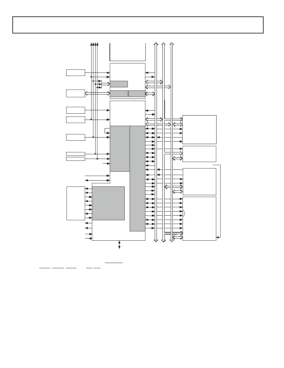
Figure 4. ADSP-TS201S Shared Memory Multiprocessing System
CLKS/REFS
ADDR310
DATA630
BR1
BR72,0
ADDR310
DATA630
BR0
BR71
BMS
CONTROL
ADSP-TS201S #0
CONTROL
ADSP-TS201S #1
ADSP-TS201S #7
ADSP-TS201S #6
ADSP-TS201S #5
ADSP-TS201S #4
ADSP-TS201S #3
ADSP-TS201S #2
RESET
RST_IN
ID20
CLKS/REFS
SCLK_V
REF
V
REF
SCLK
SCLKRAT20
000
CLOCK
REFERENCE
ADDR
DATA
HOST
PROCESSOR
INTERFACE
(OPTIONAL)
ACK
GLOBAL
MEMORY
AND
PERIPHERALS
(OPTIONAL)
OE
ADDR
DATA
CS
ADDR
DATA
BOOT
EPROM
(OPTIONAL)
RD
MS10
ACK
ID20
001
HBG
HBR
BOFF
BRST
CS
WE
WRH/L
C
O
N
T
R
O
L
A
D
D
R
E
S
S
D
A
T
A
C
O
N
T
R
O
L
A
D
D
R
E
S
S
D
A
T
A
SDRAM
MEMORY
(OPTIONAL)
MSSD30
IORD
IOEN
RAS
CAS
LDQM
HDQM
SDWE
SDCKE
SDA10
CS
RAS
CAS
DQM
WE
CKE
A10
ADDR
DATA
CLK
MSH
DMAR30
DPA
CPA
LINK
DEVICES
(4 MAX)
(OPTIONAL)
LxCLKINP/N
LxACKO
LxDATI30P/N
LxBCMPI
LxBCMPO
LxDATO30P/N
LxCLKOUTP/N
LxACKI
TMR0E
BM
CONTROLIMP10
LINK
IRQ30
FLAG30
LINK
RST_IN
BUSLOCK
CLOCK
DS20
IOWR
JTAG
POR_IN
RST_OUT
REFERENCE
LINK
DEVICES
ADSP-TS201S
Preliminary Technical Data
Rev. PrH
|
Page 9 of 40
|
December 2003
Each link port has its own triple-buffered quad-word input and
double-buffered quad-word output registers. The DSP's core
can write directly to a link port's transmit register and read from
a receive register, or the DMA controller can perform DMA
transfers through eight (four transmit and four receive) dedi-
cated link port DMA channels.
Each link port direction has three signals that control its opera-
tion. For the transmitter, LxCLKOUT is the output transmit
clock, LxACKI is the handshake input to control the data flow,
and the LxBCMPO output indicates that the block transfer is
complete. For the receiver, LxCLKIN is the input receive clock,
LxACKO is the handshake output to control the data flow, and
the LxBCMPI input indicates that the block transfer is com-
plete. The LxDATO30 pins are the data output bus for the
transmitter and the LxDATI30 pins are the input data bus for
the receiver.
Applications can program separate error detection mechanisms
for transmit and receive operations (applications can use the
checksum mechanism to implement consecutive link port
transfers), the size of data packets, and the speed at which bytes
are transmitted.
TIMER AND GENERAL-PURPOSE I/O
The ADSP-TS201S processor has a timer pin (TMR0E) that
generates output when a programmed timer counter has
expired and four programmable general-purpose I/O pins
(FLAG30) that can function as either single-bit input or out-
put. As outputs, these pins can signal peripheral devices; as
inputs, they can provide the test for conditional branching.
RESET AND BOOTING
The ADSP-TS201S processor has three levels of reset:
· Power-up reset--After power-up of the system (SCLK, all
static inputs, and strap pins are stable), the RST_IN pin
must be asserted (low).
· Normal reset--For any chip reset following the power-up
reset, the RST_IN pin must be asserted (low).
· DSP-core reset--When setting the SWRST bit in
EMUCTL, the DSP core is reset, but not the external port
or I/O.
For normal operations, tie the RST_OUT pin to the POR_IN
pin.
After reset, the ADSP-TS201S processor has four boot options
for beginning operation:
· Boot from EPROM.
· Boot by an external master (host or another ADSP-TS201S
processor).
· Boot by link port.
· No boot--Start running from memory address selected
with one of the IRQ30 interrupt signals. See
Table 2
.
Using the `no boot' option, the ADSP-TS201S processor must
start running from memory when one of the interrupts is
asserted.
The ADSP-TS201S processor core always exits from reset in the
idle state and waits for an interrupt. Some of the interrupts in
the interrupt vector table are initialized and enabled after reset.
For more information on boot options, see the EE-174: ADSP-
TS101S Booting Methods on the Analog Devices website
(
www.analog.com
)
CLOCK DOMAINS
The DSP uses calculated ratios of the SCLK clock to operate as
shown in
Figure 5
. The instruction execution rate is equal to
CCLK. A PLL from SCLK generates CCLK which is phase-
locked. The SCLKRATx pins define the clock multiplication of
SCLK to CCLK (see
Table 4 on page 13
). The link port clock is
generated from CCLK via a software programmable divisor, and
the SOC bus operates at 1/2 CCLK. Memory transfers to exter-
nal and link port buffers operate at the SOCCLK rate. SCLK also
provides clock input for the external bus interface and defines
the AC specification reference for the external bus signals. The
external bus interface runs at the SCLK frequency. The maxi-
mum SCLK frequency is one quarter the internal DSP clock
(CCLK) frequency.
POWER DOMAINS
The ADSP-TS201S processor has separate power supply con-
nections for internal logic (V
DD
), analog circuits (V
DD_A
), I/O
buffer (V
DD_IO
), and internal DRAM (V
DD_DRAM
) power supply.
Note that the analog (V
DD_A
) supply powers the clock generator
PLLs. To produce a stable clock, systems must provide a clean
power supply to power input V
DD_A
. Designs must pay critical
attention to bypassing the V
DD_A
supply.
Table 2. No Boot, Run From Memory Addresses
Interrupt
Address
IRQ0
0x3000 0000 (External Memory)
IRQ1
0x3800 0000 (External Memory)
IRQ2
0x8000 0000 (External Memory)
IRQ3
0x0000 0000 (Internal Memory)
Figure 5. Clock Domains
SCLKRATx
SCLK
SPD BITS,
LCTLx REGISTER
PLL
/2
/CR
CCLK
(INSTRUCTION RATE)
SOCCLK
(PERIPHERAL BUS RATE)
LxCLKOUT
(LINK OUTPUT RATE)
EXTERNAL INTERFACE
Rev. PrH
|
Page 10 of 40
|
December 2003
ADSP-TS201S
Preliminary Technical Data
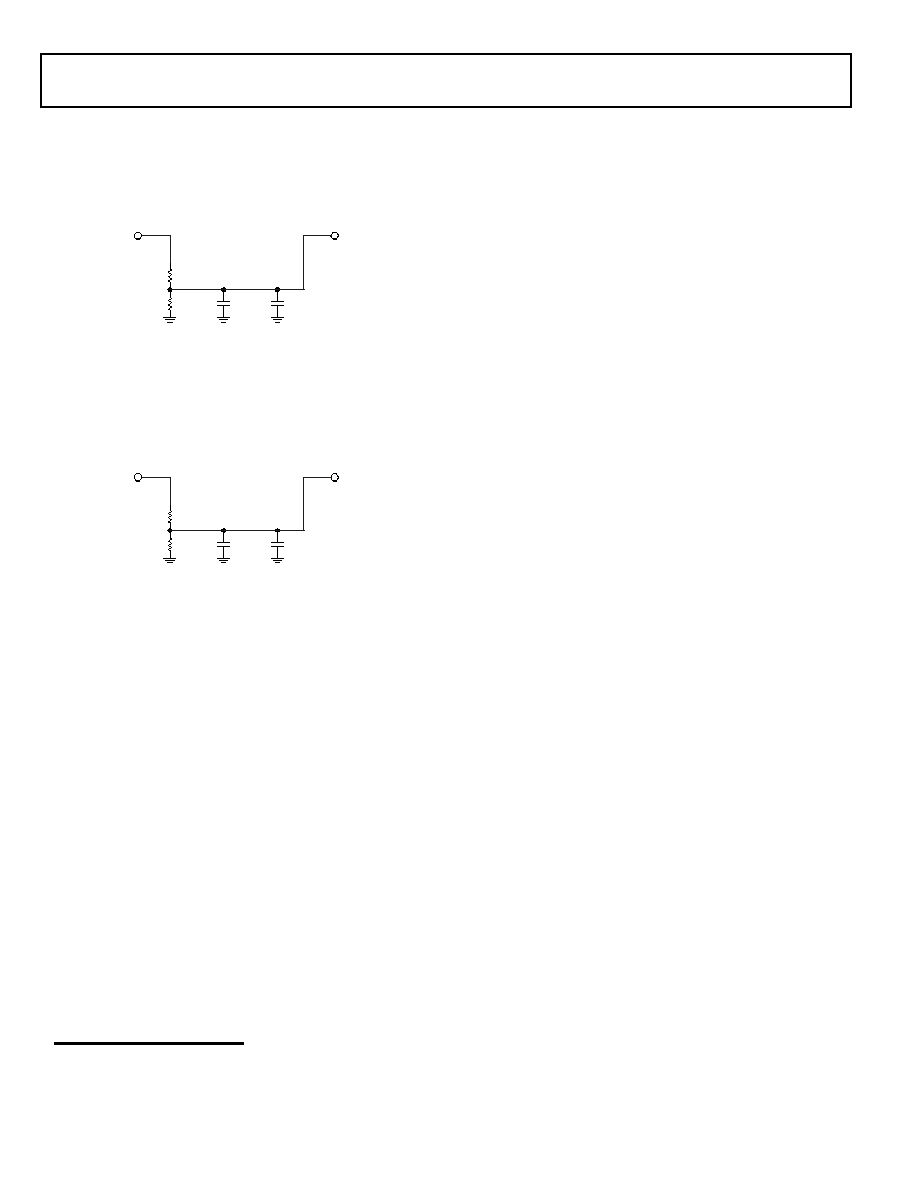
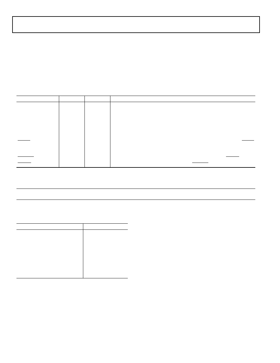
FILTERING REFERENCE VOLTAGE AND CLOCKS
Figure 6
and
Figure 7
show possible circuits for filtering V
REF
,
and SCLK_V
REF
. These circuits provide the reference voltages
for the switching voltage reference and system clock reference.
DEVELOPMENT TOOLS
The ADSP-TS201S processor is supported with a complete set
of CROSSCORE
software and hardware development tools,
including Analog Devices emulators and VisualDSP++
devel-
opment environment. The same emulator hardware that
supports other TigerSHARC processors also fully emulates the
ADSP-TS201S processor.
The VisualDSP++ project management environment lets pro-
grammers develop and debug an application. This environment
includes an easy to use assembler (which is based on an alge-
braic syntax), an archiver (librarian/library builder), a linker, a
loader, a cycle-accurate instruction-level simulator, a C/C++
compiler, and a C/C++ runtime library that includes DSP and
mathematical functions. A key point for theses tools is C/C++
code efficiency. The compiler has been developed for efficient
translation of C/C++ code to DSP assembly. The DSP has archi-
tectural features that improve the efficiency of compiled C/C++
code.
The VisualDSP++ debugger has a number of important fea-
tures. Data visualization is enhanced by a plotting package that
offers a significant level of flexibility. This graphical representa-
tion of user data enables the programmer to quickly determine
the performance of an algorithm. As algorithms grow in com-
plexity, this capability can have increasing significance on the
designer's development schedule, increasing productivity. Sta-
tistical profiling enables the programmer to nonintrusively poll
the processor as it is running the program. This feature, unique
to VisualDSP++, enables the software developer to passively
gather important code execution metrics without interrupting
the realtime characteristics of the program. Essentially, the
developer can identify bottlenecks in software quickly and effi-
ciently. By using the profiler, the programmer can focus on
those areas in the program that impact performance and take
corrective action.
Debugging both C/C++ and assembly programs with the
VisualDSP++ debugger, programmers can:
· View mixed C/C++ and assembly code (interleaved source
and object information)
· Insert breakpoints
· Set conditional breakpoints on registers, memory,
and stacks
· Trace instruction execution
· Perform linear or statistical profiling of program execution
· Fill, dump, and graphically plot the contents of memory
· Perform source level debugging
· Create custom debugger windows
The VisualDSP++ IDE lets programmers define and manage
DSP software development. Its dialog boxes and property pages
let programmers configure and manage all of the TigerSHARC
processor development tools, including the color syntax high-
lighting in the VisualDSP++ editor. This capability permit
programmers to:
· Control how the development tools process inputs and
generate outputs
· Maintain a one-to-one correspondence with the tool's
command line switches
The VisualDSP++TM Kernel (VDK) incorporates scheduling and
resource management tailored specifically to address the mem-
ory and timing constraints of DSP programming. These
capabilities enable engineers to develop code more effectively,
eliminating the need to start from the very beginning, when
developing new application code. The VDK features include
Threads, Critical and Unscheduled regions, Semaphores,
Events, and Device flags. The VDK also supports Priority-based,
Preemptive, Cooperative and Time -Sliced scheduling
approaches. In addition, the VDK was designed to be scalable. If
the application does not use a specific feature, the support code
for that feature is excluded from the target system.
Because the VDK is a library, a developer can decide whether to
use it or not. The VDK is integrated into the VisualDSP++TM
development environment, but can also be used via standard
Figure 6. V
REF
Filtering Scheme
Figure 7. SCLK_V
REF
Filtering Scheme
CROSSCORE is a registered trademark of Analog Devices, Inc.
VisualDSP++ is a registered trademark of Analog Devices, Inc.
V
DD_IO
V
SS
V
REF
R1
R2
C1
C2
R1: 2 k
SERIES RESISTOR (±1%)
R2: 2.87 k
SERIES RESISTOR (±1%)
C1: 1
F CAPACITOR (SMD)
C2: 1 nF CAPACITOR (HF SMD) PLACED CLOSE TO DSP'S PINS
CLOCK DRIVER
VOLTAGE* OR
V
DD_IO
V
SS
SCLK_V
REF
R1
R2
C1
C2
R1: 2 k
SERIES RESISTOR (±1%)
R2: 2.87 k
SERIES RESISTOR (±1%)
C1: 1
F CAPACITOR (SMD)
C2: 1 nF CAPACITOR (HF SMD) PLACED CLOSE TO DSP'S PINS
* IF CLOCK DRIVER VOLTAGE
V
DD_IO

ADSP-TS201S
Preliminary Technical Data
Rev. PrH
|
Page 11 of 40
|
December 2003
command line tools. When the VDK is used, the development
environment assists the developer with many error-prone tasks
and assists in managing system resources, automating the gen-
eration of various VDK based objects, and visualizing the
system state, when debugging an application that uses the VDK.
VCSE is Analog Devices' technology for creating, using, and
reusing software components (independent modules of sub-
stantial functionality) to quickly and reliably assemble software
applications. Download components from the Web and drop
them into the application. Publish component archives from
within VisualDSP++TM. VCSE supports component implementa-
tion in C/C++ or assembly language.
Use the Expert Linker to visually manipulate the placement of
code and data on the embedded system. View memory utiliza-
tion in a color-coded graphical form, easily move code and data
to different areas of the DSP or external memory with the drag
of the mouse, examine run-time stack and heap usage. The
Expert Linker is fully compatible with existing Linker Definition
File (LDF), allowing the developer to move between the graphi-
cal and textual environments.
Analog Devices DSP emulators use the IEEE 1149.1 JTAG Test
Access Port of the ADSP-TS201S processor to monitor and con-
trol the target board processor during emulation. The emulator
provides full speed emulation, allowing inspection and modifi-
cation of memory, registers, and processor stacks. Nonintrusive
in-circuit emulation is assured by the use of the processor's
JTAG interface--the emulator does not affect target system
loading or timing.
In addition to the software and hardware development tools
available from Analog Devices, third parties provide a wide
range of tools supporting the TigerSHARC processor family.
Hardware tools include TigerSHARC processor PC plug-in
cards. Third party software tools include DSP libraries, real-
time operating systems, and block diagram design tools.
DESIGNING AN EMULATOR-COMPATIBLE DSP
BOARD (TARGET)
The Analog Devices family of emulators are tools that every
DSP developer needs to test and debug hardware and software
systems. Analog Devices has supplied an IEEE 1149.1 JTAG
Test Access Port (TAP) on each JTAG DSP. The emulator uses
the TAP to access the internal features of the DSP, allowing the
developer to load code, set breakpoints, observe variables,
observe memory, and examine registers. The DSP must be
halted to send data and commands, but once an operation has
been completed by the emulator, the DSP system is set running
at full speed with no impact on system timing.
To use these emulators, the target board must include a header
that connects the DSP's JTAG port to the emulator.
For details on target board design issues including mechanical
layout, single processor connections, multiprocessor scan
chains, signal buffering, signal termination, and emulator pod
logic, see the EE-68: Analog Devices JTAG Emulation Technical
Reference on the Analog Devices website (
www.analog.com
)--
use site search on "EE-68". This document is updated regularly
to keep pace with improvements to emulator support.
ADDITIONAL INFORMATION
This data sheet provides a general overview of the ADSP-
TS201S processor's architecture and functionality. For detailed
information on the ADSP-TS201S processor's core architecture
and instruction set, see the ADSP-TS201 TigerSHARC Processor
Hardware Reference and the ADSP-TS201 TigerSHARC Proces-
sor Programming Reference. For detailed information on the
development tools for this processor, see the VisualDSP++
User's Guide for TigerSHARC Processors.
Rev. PrH
|
Page 12 of 40
|
December 2003
ADSP-TS201S
Preliminary Technical Data
PIN FUNCTION DESCRIPTIONS
While most of the ADSP-TS201S processor's input pins are nor-
mally synchronous--tied to a specific clock--a few are
asynchronous. For these asynchronous signals, an on-chip syn-
chronization circuit prevents metastability problems. Use the
AC specification for asynchronous signals when the system
design requires predictable, cycle-by-cycle behavior for these
signals.
The output pins can be three-stated during normal operation.
The DSP three-states all outputs during reset, allowing these
pins to get to their internal pullup or pulldown state. Some pins
have an internal pullup or pulldown resistor (±30% tolerance)
that maintains a known value during transitions between differ-
ent drivers.
Table 3. Pin Definitions--Clocks and Reset
Signal
Type
Term
Description
SCLKRAT20
I (pd)
au
Core Clock Ratio. The DSP's core clock (CCLK) rate = n × SCLK, where n is user-
programmable using the SCLKRATx pins to the values shown in
Table 4
. These pins
must have a constant value while the DSP is powered. The core clock rate (CCLK) is
the instruction cycle rate.
SCLK
I
1
au
System Clock Input. The DSP's system input clock for cluster bus.The core clock rate
is user-programmable using the SCLKRATx pins.
For more information, see Clock
Domains on page 9.
RST_IN
I/A
au
Reset. Sets the DSP to a known state and causes program to be in idle state. RST_IN
must be asserted a specified time according to the type of reset operation. For details,
see
Reset and Booting on page 9
,
Table 19 on page 24
, and
Figure 9 on page 25
.
RST_OUT
O
au
Reset Output. Indicates that the DSP reset is complete. Connect to POR_IN.
POR_IN
I/A
au
Power On Reset for internal DRAM. Connect to RST_OUT.
I = input; A = asynchronous; O = output; OD = open drain output; T = Three-State; P = power supply; G = ground;
pd = internal pulldown 5 k
; pu = internal pullup 5 k
; pd_0 = internal pulldown 5 k
on DSP ID=0; pu_0 = internal pullup 5 k
on DSP
ID=0; pu_od_0 = internal pullup 500
on DSP ID=0; pd_m = internal pulldown 5 k
on DSP bus master; pu_m = internal pullup 5 k
on DSP
bus master; pu_ad = internal pullup 40 k
; For more pulldown and pullup information, see
Electrical Characteristics on page 22
.
Term (for termination) column symbols: epd = External pull-down approximately 5 k
to V
SS
; epu = External pull-up approximately 5 k
to V
DD_IO
, nc = Not connected; au = Always used.
1
For more information on SCLK and SCLK_V
REF
on revision 0.x silicon, see the EE-179: ADSP-TS20x TigerSHARC System Design Guidelines on the Analog Devices website
(
www.analog.com
).
Table 4. SCLK Ratio
SCLKRAT20
Ratio
000 (default)
4
001
5
010
6
011
7
100
8
101
10
110
12
111
Reserved

ADSP-TS201S
Preliminary Technical Data
Rev. PrH
|
Page 13 of 40
|
December 2003
Table 5. Pin Definitions--External Port Bus Controls
Signal
Type
Term
Description
ADDR310
I/O/T
(pu_ad)
nc
Address Bus. The DSP issues addresses for accessing memory and peripherals on
these pins. In a multiprocessor system, the bus master drives addresses for accessing
internal memory or I/O processor registers of other ADSP-TS201S processors. The DSP
inputs addresses when a host or another DSP accesses its internal memory or I/O
processor registers.
DATA630
I/O/T
(pu_ad)
nc
External Data Bus. The DSP drives and receives data and instructions on these pins.
Pullup/down resistors on unused DATA pins are unnecessary.
RD
I/O/T
(pu_0)
epu
Memory Read. RD is asserted whenever the DSP reads from any slave in the system,
excluding SDRAM. When the DSP is a slave, RD is an input and indicates read trans-
actions that access its internal memory or universal registers. In a multiprocessor
system, the bus master drives RD. RD changes concurrently with ADDR pins.
WRL
I/O/T
(pu_0)
epu
Write Low. WRL is asserted in two cases: When the ADSP-TS201S processor writes to
an even address word of external memory or to another external bus agent; and when
the ADSP-TS201S processor writes to a 32-bit zone (host, memory or DSP
programmed to 32-bit bus). An external master (host or DSP) asserts WRL for writing
to a DSP's low word of internal memory. In a multiprocessor system, the bus master
drives WRL. WRL changes concurrently with ADDR pins. When the DSP is a slave, WRL
is an input and indicates write transactions that access its internal memory or
universal registers.
WRH
I/O/T
(pu_0)
epu
Write High. WRH is asserted when the ADSP-TS201S processor writes a long word (64
bits) or writes to an odd address word of external memory or to another external bus
agent on a 64-bit data bus. An external master (host or another DSP) must assert WRH
for writing to a DSP's high word of 64-bit data bus. In a multiprocessing system, the
bus master drives WRH. WRH changes concurrently with ADDR pins. When the DSP
is a slave, WRH is an input and indicates write transactions that access its internal
memory or universal registers.
ACK
I/O/T/OD
(pu_od_0)
epu
Acknowledge. External slave devices can de-assert ACK to add wait states to external
memory accesses. ACK is used by I/O devices, memory controllers and other periph-
erals on the data phase. The DSP can de-assert ACK to add wait states to read and
write accesses of its internal memory. The pullup is 50
on low-to-high transactions
and is 500
on all other transactions.
BMS
O/T
(pu_0)
au
Boot Memory Select. BMS is the chip select for boot EPROM or flash memory. During
reset, the DSP uses BMS as a strap pin (EBOOT) for EPROM boot mode. In a multipro-
cessor system, the DSP bus master drives BMS. For details, see
Reset and Booting on
page 9
and see the EBOOT signal description in
Table 15 on page 20
.
MS10
O/T
(pu_0)
nc
Memory Select. MS0 or MS1 is asserted whenever the DSP accesses memory banks 0
or 1 respectively. MS10 are decoded memory address pins that change concurrently
with ADDR pins. When ADDR31:27 = 0b00110, MS0 is asserted. When ADDR31:27 =
0b00111, MS1 is asserted. In multiprocessor systems, the master DSP drives MS10.
MSH
O/T
(pu_0)
nc
Memory Select Host. MSH is asserted whenever the DSP accesses the host address
space (ADDR31 = 0b1). MSH is a decoded memory address pin that changes concur-
rently with ADDR pins. In a multiprocessor system, the bus master DSP drives MSH.
BRST
I/O/T
(pu_0)
epu
Burst. The current bus master (DSP or host) asserts this pin to indicate that it is reading
or writing data associated with consecutive addresses. A slave device can ignore
addresses after the first one and increment an internal address counter after each
transfer. For host-to-DSP burst accesses, the DSP increments the address automati-
cally while BRST is asserted.
I = input; A = asynchronous; O = output; OD = open drain output; T = Three-State; P = power supply; G = ground;
pd = internal pulldown 5 k
; pu = internal pullup 5 k
; pd_0 = internal pulldown 5 k
on DSP ID=0; pu_0 = internal pullup 5 k
on DSP
ID=0; pu_od_0 = internal pullup 500
on DSP ID=0; pd_m = internal pulldown 5 k
on DSP bus master; pu_m = internal pullup 5 k
on DSP
bus master; pu_ad = internal pullup 40 k
; For more pulldown and pullup information, see
Electrical Characteristics on page 22
.
Term (for termination) column symbols: epd = External pull-down approximately 5 k
to V
SS
; epu = External pull-up approximately 5 k
to V
DD_IO
, nc = Not connected; au = Always used.
Rev. PrH
|
Page 14 of 40
|
December 2003
ADSP-TS201S
Preliminary Technical Data
Table 6. Pin Definitions--External Port Arbitration
Signal
Type
Term
Description
BR70
I/O
V
DD_IO
Multiprocessing Bus Request Pins. Used by the DSPs in a multiprocessor system to
arbitrate for bus mastership. Each DSP drives its own BRx line (corresponding to the
value of its ID20 inputs) and monitors all others. In systems with fewer than eight
DSPs, set the unused BRx pins high (V
DD_IO
).
ID20
I (pd)
au
Multiprocessor ID. Indicates the DSP's ID, from which the DSP determines its order in
a multiprocessor system. These pins also indicate to the DSP which bus request
(BR0BR7) to assert when requesting the bus: 000 = BR0, 001 = BR1, 010 = BR2,
011 = BR3, 100 = BR4, 101 = BR5, 110 = BR6, or 111 = BR7. ID20 must have a constant
value during system operation and can change during reset only.
BM
O
au
Bus Master. The current bus master DSP asserts BM. For debugging only. At reset this
is a strap pin. For more information, see
Table 15 on page 20
.
BOFF
I
epu
Back Off. A deadlock situation can occur when the host and a DSP try to read from
each other's bus at the same time. When deadlock occurs, the host can assert BOFF
to force the DSP to relinquish the bus before completing its outstanding transaction.
BUSLOCK
O/T
(pu_0)
au
Bus Lock Indication. Provides an indication that the current bus master has locked
the bus. At reset, this is a strap pin. For more information, see
Table 15 on page 20
.
HBR
I
epu
Host Bus Request. A host must assert HBR to request control of the DSP's external bus.
When HBR is asserted in a multiprocessing system, the bus master relinquishes the
bus and asserts HBG once the outstanding transaction is finished.
HBG
I/O/T
(pu_0)
epu
1
Host Bus Grant. Acknowledges HBR and indicates that the host can take control of
the external bus. When relinquishing the bus, the master DSP three-states the
ADDR310, DATA630, MSH, MSSD30, MS10, RD, WRL, WRH, BMS, BRST, IORD,
IOWR, IOEN, RAS, CAS, SDWE, SDA10, SDCKE, LDQM and HDQM pins, and the DSP puts
the SDRAM in self-refresh mode. The DSP asserts HBG until the host deasserts HBR.
In multiprocessor systems, the current bus master DSP drives HBG, and all slave DSPs
monitor it.
CPA
I/O/OD
(pu_od_0)
epu
Core Priority Access. Asserted while the DSP's core accesses external memory. This
pin enables a slave DSP to interrupt a master DSP's background DMA transfers and
gain control of the external bus for core-initiated transactions. CPA is an open drain
output, connected to all DSPs in the system. If not required in the system, leave CPA
unconnected (external pullups will be required for DSP ID=1 through ID=7).
DPA
I/O/OD
(pu_od_0)
epu
DMA Priority Access. Asserted while a high-priority DSP DMA channel accesses
external memory. This pin enables a high-priority DMA channel on a slave DSP to
interrupt transfers of a normal-priority DMA channel on a master DSP and gain control
of the external bus for DMA-initiated transactions. DPA is an open drain output,
connected to all DSPs in the system. If not required in the system, leave DPA uncon-
nected (external pullups will be required for DSP ID=1 through ID=7).
I = input; A = asynchronous; O = output; OD = open drain output; T = Three-State; P = power supply; G = ground;
pd = internal pulldown 5 k
; pu = internal pullup 5 k
; pd_0 = internal pulldown 5 k
on DSP ID=0; pu_0 = internal pullup 5 k
on DSP
ID=0; pu_od_0 = internal pullup 500
on DSP ID=0; pd_m = internal pulldown 5 k
on DSP bus master; pu_m = internal pullup 5 k
on DSP
bus master; pu_ad = internal pullup 40 k
; For more pulldown and pullup information, see
Electrical Characteristics on page 22
.
Term (for termination) column symbols: epd = External pull-down approximately 5 k
to V
SS
; epu = External pull-up approximately 5 k
to V
DD_IO
, nc = Not connected; au = Always used.
1
This external pull-up resistor may be omitted for the ID=000 TigerSHARC processor.
ADSP-TS201S
Preliminary Technical Data
Rev. PrH
|
Page 15 of 40
|
December 2003
Table 7. Pin Definitions--External Port DMA/Flyby
Signal
Type
Term
Description
DMAR30
I/A
epu
DMA Request Pins. Enable external I/O devices to request DMA services from the DSP.
In response to DMARx, the DSP performs DMA transfers according to the DMA
channel's initialization. The DSP ignores DMA requests from uninitialized channels.
IOWR
O/T
(pu_0)
nc
I/O Write. When a DSP DMA channel initiates a flyby mode read transaction, the DSP
asserts the IOWR signal during the data cycles. This assertion makes the I/O device
sample the data instead of the TigerSHARC.
IORD
O/T
(pu_0)
nc
I/O Read. When a DSP DMA channel initiates a flyby mode write transaction, the DSP
asserts the IORD signal during the data cycle. This assertion with the IOEN makes the
I/O device drive the data instead of the TigerSHARC.
IOEN
O/T
(pu_0)
nc
I/O Device Output Enable. Enables the output buffers of an external I/O device for fly-
by transactions between the device and external memory. Active on fly-by
transactions.
I = input; A = asynchronous; O = output; OD = open drain output; T = Three-State; P = power supply; G = ground;
pd = internal pulldown 5 k
; pu = internal pullup 5 k
; pd_0 = internal pulldown 5 k
on DSP ID=0; pu_0 = internal pullup 5 k
on DSP
ID=0; pu_od_0 = internal pullup 500
on DSP ID=0; pd_m = internal pulldown 5 k
on DSP bus master; pu_m = internal pullup 5 k
on DSP
bus master; pu_ad = internal pullup 40 k
; For more pulldown and pullup information, see
Electrical Characteristics on page 22
.
Term (for termination) column symbols: epd = External pull-down approximately 5 k
to V
SS
; epu = External pull-up approximately 5 k
to V
DD_IO
, nc = Not connected; au = Always used.
Table 8. Pin Definitions--External Port SDRAM Controller
Signal
Type
Term
Description
MSSD30
I/O/T
(pu_0)
nc
Memory Select SDRAM. MSSD0, MSSD1, MSSD2, or MSSD3 is asserted whenever the
DSP accesses SDRAM memory space. MSSD30 are decoded memory address pins
that are asserted whenever the DSP issues an SDRAM command cycle (access to
ADDR31:30 = 0b01--except reserved spaces shown in
Figure 3 on page 6
). In a multi-
processor system, the master DSP drives MSSD30.
RAS
I/O/T
(pu_0)
nc
Row Address Select. When sampled low, RAS indicates that a row address is valid in
a read or write of SDRAM. In other SDRAM accesses, it defines the type of operation
to execute according to SDRAM specification.
CAS
I/O/T
(pu_0)
nc
Column Address Select. When sampled low, CAS indicates that a column address is
valid in a read or write of SDRAM. In other SDRAM accesses, it defines the type of
operation to execute according to the SDRAM specification.
LDQM
O/T
(pu_0)
nc
Low Word SDRAM Data Mask. When sampled high, three-states the SDRAM DQ
buffers. LDQM is valid on SDRAM transactions when CAS is asserted, and inactive on
read transactions. On write transactions, LDQM is active when accessing an odd
address word on a 64-bit memory bus to disable the write of the low word.
HDQM
O/T
(pu_0)
nc
High Word SDRAM Data Mask. When sampled high, three-states the SDRAM DQ
buffers. HDQM is valid on SDRAM transactions when CAS is asserted, and inactive on
read transactions. On write transactions, HDQM is active when accessing an even
address in word accesses or when memory is configured for a 32-bit bus to disable
the write of the high word.
I = input; A = asynchronous; O = output; OD = open drain output; T = Three-State; P = power supply; G = ground;
pd = internal pulldown 5 k
; pu = internal pullup 5 k
; pd_0 = internal pulldown 5 k
on DSP ID=0; pu_0 = internal pullup 5 k
on DSP
ID=0; pu_od_0 = internal pullup 500
on DSP ID=0; pd_m = internal pulldown 5 k
on DSP bus master; pu_m = internal pullup 5 k
on DSP
bus master; pu_ad = internal pullup 40 k
; For more pulldown and pullup information, see
Electrical Characteristics on page 22
.
Term (for termination) column symbols: epd = External pull-down approximately 5 k
to V
SS
; epu = External pull-up approximately 5 k
to V
DD_IO
, nc = Not connected; au = Always used.
Rev. PrH
|
Page 16 of 40
|
December 2003
ADSP-TS201S
Preliminary Technical Data
SDA10
O/T
(pu_0)
nc
SDRAM Address bit 10 pin. Separate A10 signals enable SDRAM refresh operation
while the DSP executes non-SDRAM transactions.
SDCKE
I/O/T
(pu_m/
pd_m)
nc
SDRAM Clock Enable. Activates the SDRAM clock for SDRAM self-refresh or suspend
modes. A slave DSP in a multiprocessor system does not have the pullup or pulldown.
A master DSP (or ID=0 in a single processor system) has a pullup before granting the
bus to the host, except when the SDRAM is put in self refresh mode. In self refresh
mode, the master has a pulldown before granting the bus to the host.
SDWE
I/O/T
(pu_0)
nc
SDRAM Write Enable. When sampled low while CAS is active, SDWE indicates an
SDRAM write access. When sampled high while CAS is active, SDWE indicates an
SDRAM read access. In other SDRAM accesses, SDWE defines the type of operation to
execute according to SDRAM specification.
Table 9. Pin Definitions--JTAG Port
Signal
Type
Term
Description
EMU
O/OD
nc
1
Emulation. Connected to the DSP's JTAG emulator target board connector only.
TCK
I
epd or epu
1
Test Clock (JTAG). Provides an asynchronous clock for JTAG scan.
TDI
I
(pu_ad)
nc
1
Test Data Input (JTAG). A serial data input of the scan path.
TDO
O/T
nc
1
Test Data Output (JTAG). A serial data output of the scan path.
TMS
I
(pu_ad)
nc
1
Test Mode Select (JTAG). Used to control the test state machine.
TRST
I/A
(pu_ad)
au
Test Reset (JTAG). Resets the test state machine. TRST must be asserted or pulsed low
after power up for proper device operation. For more information, see
Reset and
Booting on page 9
.
I = input; A = asynchronous; O = output; OD = open drain output; T = Three-State; P = power supply; G = ground;
pd = internal pulldown 5 k
; pu = internal pullup 5 k
; pd_0 = internal pulldown 5 k
on DSP ID=0; pu_0 = internal pullup 5 k
on DSP
ID=0; pu_od_0 = internal pullup 500
on DSP ID=0; pd_m = internal pulldown 5 k
on DSP bus master; pu_m = internal pullup 5 k
on DSP
bus master; pu_ad = internal pullup 40 k
; For more pulldown and pullup information, see
Electrical Characteristics on page 22
Term (for termination) column symbols: epd = External pull-down approximately 5 k
to V
SS
; epu = External pull-up approximately 5 k
to V
DD_IO
, nc = Not connected; au = Always used.
1
See the reference
on page 11
to the JTAG emulation technical reference EE-68.
Table 8. Pin Definitions--External Port SDRAM Controller (Continued)
Signal
Type
Term
Description
I = input; A = asynchronous; O = output; OD = open drain output; T = Three-State; P = power supply; G = ground;
pd = internal pulldown 5 k
; pu = internal pullup 5 k
; pd_0 = internal pulldown 5 k
on DSP ID=0; pu_0 = internal pullup 5 k
on DSP
ID=0; pu_od_0 = internal pullup 500
on DSP ID=0; pd_m = internal pulldown 5 k
on DSP bus master; pu_m = internal pullup 5 k
on DSP
bus master; pu_ad = internal pullup 40 k
; For more pulldown and pullup information, see
Electrical Characteristics on page 22
.
Term (for termination) column symbols: epd = External pull-down approximately 5 k
to V
SS
; epu = External pull-up approximately 5 k
to V
DD_IO
, nc = Not connected; au = Always used.
ADSP-TS201S
Preliminary Technical Data
Rev. PrH
|
Page 17 of 40
|
December 2003
Table 10. Pin Definitions--Flags, Interrupts, and Timer
Signal
Type
Term
Description
FLAG30
I/O/A
(pu)
nc
FLAG pins. Bidirectional input/output pins can be used as program conditions. Each pin
can be configured individually for input or for output. FLAG30 are inputs after power-up
and reset.
IRQ30
I/A
(pu)
nc
Interrupt Request. When asserted, the DSP generates an interrupt. Each of the IRQ30 pins
can be independently set for edge-triggered or level-sensitive operation. After reset, these
pins are disabled unless the IRQ30 strap option and interrupt vectors are initialized for
booting.
TMR0E
O
au
Timer 0 expires. This output pulses whenever timer 0 expires. At reset, this is a strap pin.
For more information, see
Table 15 on page 20
.
I = input; A = asynchronous; O = output; OD = open drain output; T = Three-State; P = power supply; G = ground;
pd = internal pulldown 5 k
; pu = internal pullup 5 k
; pd_0 = internal pulldown 5 k
on DSP ID=0; pu_0 = internal pullup 5 k
on DSP
ID=0; pu_od_0 = internal pullup 500
on DSP ID=0; pd_m = internal pulldown 5 k
on DSP bus master; pu_m = internal pullup 5 k
on DSP
bus master; pu_ad = internal pullup 40 k
; For more pulldown and pullup information, see
Electrical Characteristics on page 22
.
Term (for termination) column symbols: epd = External pull-down approximately 5 k
to V
SS
; epu = External pull-up approximately 5 k
to V
DD_IO
, nc = Not connected; au = Always used.
Table 11. Pin Definitions--Link Ports
Signal
Type
Term
Description
LxDATO30P
O
nc
Link Ports 30 Data 30 Transmit LVDS P
LxDATO30N
O
nc
Link Ports 30 Data 30 Transmit LVDS N
LxCLKOUTP
O
nc
Link Ports 30 Transmit Clock LVDS P
LxCLKOUTN
O
nc
Link Ports 30 Transmit Clock LVDS N
LxACKI
I (pd)
nc
Link Ports 30 Receive Acknowledge. Using this signal, the receiver indicates to the
transmitter that it may continue the transmission
LxBCMPO
O
nc
1
Link Ports 30 Block Completion. When the transmission is executed using DMA, this
signal indicates to the receiver that the transmitted block is completed. At reset, the
L1BCMPO, L2BCMPO, and L3BCMPO pins are strap pins. For more information, see
Table 15 on page 20
.
LxDATI30P
I
V
DD_IO
Link Ports 30 Data 30 Receive LVDS P
LxDATI30N
I
V
DD_IO
Link Ports 30 Data 30 Receive LVDS N
LxCLKINP
I/A
V
DD_IO
Link Ports 30 Receive Clock LVDS P
LxCLKINN
I/A
V
SS
Link Ports 30 Receive Clock LVDS N
LxACKO
O
nc
Link Ports 30 Transmit Acknowledge. Using this signal, the receiver indicates to the
transmitter that it may continue the transmission.
LxBCMPI
I
V
SS
Link Ports 30 Block Completion. When the reception is executed using DMA, this
signal indicates to the transmitter that the receive block is completed.
I = input; A = asynchronous; O = output; OD = open drain output; T = Three-State; P = power supply; G = ground;
pd = internal pulldown 5 k
; pu = internal pullup 5 k
; pd_0 = internal pulldown 5 k
on DSP ID=0; pu_0 = internal pullup 5 k
on DSP
ID=0; pu_od_0 = internal pullup 500
on DSP ID=0; pd_m = internal pulldown 5 k
on DSP bus master; pu_m = internal pullup 5 k
on DSP
bus master; pu_ad = internal pullup 40 k
; For more pulldown and pullup information, see
Electrical Characteristics on page 22
.
Term (for termination) column symbols: epd = External pull-down approximately 5 k
to V
SS
; epu = External pull-up approximately 5 k
to V
DD_IO
, nc = Not connected; au = Always used.
1
The L1BCMPO and L2BCMPO pins have different termination requirements on revision 0.x silicon, see the EE-179: ADSP-TS20xS TigerSHARC System Design Guidelines
on the Analog Devices website (
www.analog.com
).
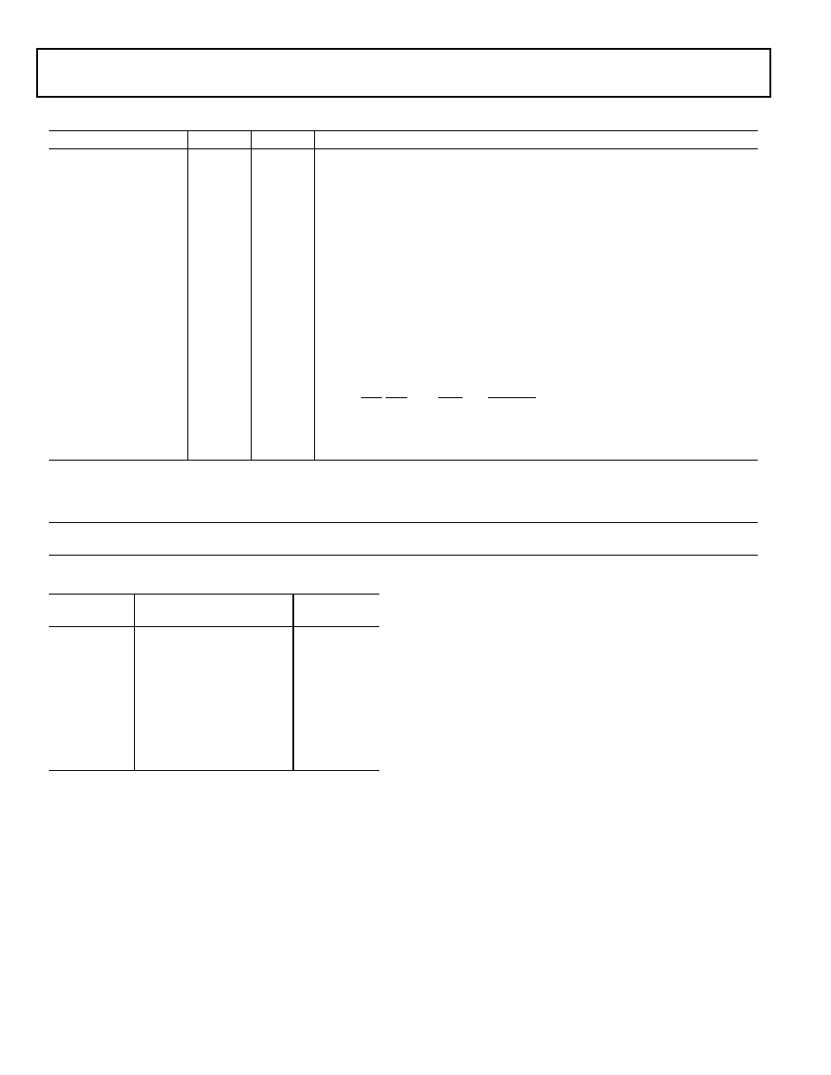
Rev. PrH
|
Page 18 of 40
|
December 2003
ADSP-TS201S
Preliminary Technical Data
Table 12. Pin definitions--Impedance Control , Drive Strength Control, and Regulator Enable
Signal
Type
Term
Description
CONTROLIMP0
I (pd)
au
Impedance Control. CONTROLIMP0 enables Pulse Mode. When CONTROLIMP0 = 0,
Pulse Mode is disabled and the output drive strength is continuously controlled by
DS20, both in the digital mode and in the analog mode (See analog and digital modes
below). When CONTROLIMP0 = 1, Pulse Mode is enabled. In Pulse Mode, whenever a
new value is driven to the output pin, drive strength is set to 100% for a short period of
1.5-2.5ns after rising edge of SCLK and afterwards it is set back to the value defined by
the resistance control DS20 pins as shown in
Table 13
.
CONTROLIMP1
I (pu)
au
Impedance Control. CONTROLIMP1 enables A/D mode of the control impedance
circuitry.When CONTROLIMP1 = 0, A/D mode is disabled, and output drive strength is
set relative to maximum drive strength according to table in DS20 explanation. When
CONTROLIMP1 = 1, A/D mode is enabled, and the resistance control operates in the
analog mode, where drive strength is continuously controlled to match a specific line
impedance as shown in
Table 13
.
DS2,0
DS1
I (pu)
I (pd)
au
Digital Drive Strength Selection. Selected as shown in
Table 13
. For drive strength calcu-
lation, see
Output Drive Currents on page 33
. The drive strength for some pins is preset,
not controlled by the DS20 pins. The pins that are always at drive strength 7 (100%)
include: CPA, DPA, TDO, EMU, and RST_OUT. The drive strength for the ACK pin is always
x2 drive strength 7 (100%).
ENEDREG
I (pu)
V
SS
Enable on-chip DRAM Regulator. Connect the ENEDREG pin to V
SS
. Connect the V
DD_DRAM
pins to a properly decoupled DRAM power supply.
I = input; A = asynchronous; O = output; OD = open drain output; T = Three-State; P = power supply; G = ground;
pd = internal pulldown 5 k
; pu = internal pullup 5 k
; pd_0 = internal pulldown 5 k
on DSP ID=0; pu_0 = internal pullup 5 k
on DSP
ID=0; pu_od_0 = internal pullup 500
on DSP ID=0; pd_m = internal pulldown 5 k
on DSP bus master; pu_m = internal pullup 5 k
on DSP
bus master; pu_ad = internal pullup 40 k
; For more pulldown and pullup information, see
Electrical Characteristics on page 22
.
Term (for termination) column symbols: epd = External pull-down approximately 5 k
to V
SS
; epu = External pull-up approximately 5 k
to V
DD_IO
, nc = Not connected; au = Always used.
Table 13. Drive Strength/Output Impedance Selection
DS20
Pins
Drive
Strength
1
Output
Impedance
2
000
Strength 0 (11.1%)
26
001
Strength 1 (23.8%)
32
010
Strength 2 (36.5%)
40
011
Strength 3 (49.2%)
50
100
Strength 4 (61.9%)
62
101 (default)
Strength 5 (74.6%)
70
110
Strength 6 (87.3%)
96
111
Strength 7 (100%)
120
1
CONTROLIMP1 = 0, A/D mode disabled.
2
CONTROLIMP1 = 1, A/D mode enabled.
ADSP-TS201S
Preliminary Technical Data
Rev. PrH
|
Page 19 of 40
|
December 2003
STRAP PIN FUNCTION DESCRIPTIONS
Some pins have alternate functions at reset. Strap options set
DSP operating modes. During reset, the DSP samples the strap
option pins. Strap pins have an internal pullup or pulldown for
the default value. If a strap pin is not connected to an overdriv-
ing external pullup, pulldown, or logic load, the DSP samples
the default value during reset. If strap pins are connected to
logic inputs, a stronger external pullup or pulldown may be
required to ensure default value depending on leakage and/or
low level input current of the logic load. To set a mode other
than the default mode, connect the strap pin to a sufficiently
stronger external pullup or pulldown.
Table 15
lists and
describes each of the DSP's strap pins.
Table 14. Pin Definitions--Power, Ground, and Reference
Signal
Type
Term
Description
V
DD
P
au
V
DD
pins for internal logic.
V
DD_A
P
au
V
DD
pins for analog circuits. Pay critical attention to bypassing this supply.
V
DD_IO
P
au
V
DD
pins for I/O buffers.
V
DD_DRAM
P
au
V
DD
pins for internal DRAM.
V
REF
I
au
Reference voltage defines the trip point for all input buffers, except SCLK, RST_IN,
POR_IN, IRQ30, FLAG30, DMAR30, ID20, CONTROLIMP10, LxDATO30P/N,
LxCLKOUTP/N, LxDATI30P/N, LxCLKINP/N, TCK, TDI, TMS, and TRST. V
REF
can be
connected to a power supply or set by a voltage divider circuit as shown in
Figure 6
.
For more information, see Filtering Reference Voltage and Clocks on page 10.
SCLK_V
REF
I
1
au
System Clock Reference. Connect this pin to a reference voltage as shown in
Figure 7
.
For more information, see Filtering Reference Voltage and Clocks on page 10.
V
SS
G
au
Ground pins.
NC
--
nc
No Connect. Do not connect these pins to anything (not to any supply, signal, or each
other). These pins are reserved and must be left unconnected.
I = input; A = asynchronous; O = output; OD = open drain output; T = Three-State; P = power supply; G = ground;
pd = internal pulldown 5 k
; pu = internal pullup 5 k
; pd_0 = internal pulldown 5 k
on DSP ID=0; pu_0 = internal pullup 5 k
on DSP
ID=0; pu_od_0 = internal pullup 500
on DSP ID=0; pd_m = internal pulldown 5 k
on DSP bus master; pu_m = internal pullup 5 k
on DSP
bus master; pu_ad = internal pullup 40 k
; For more pulldown and pullup information, see
Electrical Characteristics on page 22
.
Term (for termination) column symbols: epd = External pull-down approximately 5 k
to V
SS
; epu = External pull-up approximately 5 k
to V
DD_IO
, nc = Not connected; au = Always used.
1
For more information on SCLK and SCLK_V
REF
on revision 0.0 silicon, see the EE-179: ADSP-TS20xS TigerSHARC System Design Guidelines on the Analog Devices website
(
www.analog.com
).
Table 15. Pin Definitions--I/O Strap Pins
Signal
Type (at
Reset)
On Pin...
Description
EBOOT
I
(pd_0)
BMS
EPROM boot.
0 = boot from EPROM immediately after reset (default)
1 = idle after reset and wait for an external device to boot DSP
through the external port or a link port
IRQEN
I
(pd)
BM
Interrupt Enable.
0 = disable and set IRQ30 interrupts to level-sensitive after
reset (default)
1 = enable and set IRQ30 interrupts to edge-sensitive
immediately after reset
LINK_DWIDTH
I
(pd)
TMR0E
Link Port Input Default Data Width.
0 = 1-bit (default)
1 = 4-bit
I = input; A = asynchronous; O = output; OD = open drain output; T = Three-State; P = power supply; G = ground;
pd = internal pulldown 5 k
; pu = internal pullup 5 k
; pd_0 = internal pulldown 5 k
on DSP ID=0; pu_0 = internal pullup 5 k
on DSP
ID=0; pu_od_0 = internal pullup 500
on DSP ID=0; pd_m = internal pulldown 5 k
on DSP bus master; pu_m = internal pullup 5 k
on DSP
bus master; pu_ad = internal pullup 40 k
; For more pulldown and pullup information, see
Electrical Characteristics on page 22
.
Rev. PrH
|
Page 20 of 40
|
December 2003
ADSP-TS201S
Preliminary Technical Data
When default configuration is used, no external resistor is
needed on the strap pins. To apply other configurations, a 500
resistor connected to V
DD_IO
is required. If providing external
pulldowns, do not strap these pins directly to V
SS
; the strap pins
require 500
resistor straps.
All strap pins are sampled on the rising edge of RST_IN (de-
assertion edge). Each pin latches the strapped pin state (state of
the strap pin at the rising edge of RST_IN). Shortly after de-
assertion of RST_IN, these pins are re-configured to their nor-
mal functionality.
These strap pins have an internal pull-down resistor, pull-up
resistor, or no-resistor (three-state) on each pin. The resistor
type, which is connected to the I/O pad, depends on whether
RST_IN is active (low) or if RST_IN is de-asserted (high).
Table 16
shows the resistors that are enabled during active reset
and during normal operation.
SYS_REG_WE
I
(pd_0)
BUSLOCK
SYSCON and SDRCON Write Enable.
0 = one-time writable after reset (default)
1 = always writable
TM1
I
(pu)
L1BCMPO
Test Mode 1. Do not overdrive default value during reset.
TM2
I
(pu)
L2BCMPO
Test Mode 2. Do not overdrive default value during reset.
TM3
I
(pu)
L3BCMPO
Test Mode 3. Do not overdrive default value during reset.
Table 15. Pin Definitions--I/O Strap Pins (Continued)
Signal
Type (at
Reset)
On Pin...
Description
I = input; A = asynchronous; O = output; OD = open drain output; T = Three-State; P = power supply; G = ground;
pd = internal pulldown 5 k
; pu = internal pullup 5 k
; pd_0 = internal pulldown 5 k
on DSP ID=0; pu_0 = internal pullup 5 k
on DSP
ID=0; pu_od_0 = internal pullup 500
on DSP ID=0; pd_m = internal pulldown 5 k
on DSP bus master; pu_m = internal pullup 5 k
on DSP
bus master; pu_ad = internal pullup 40 k
; For more pulldown and pullup information, see
Electrical Characteristics on page 22
.
Table 16. Strap Pin Internal Resistors--Active Reset
(RST_IN = 0) Versus Normal Operation (RST_IN = 1)
PIN
RST_IN = 0
RST_IN = 1
BMS
(pd_0)
(pu_0)
BM
(pd)
Driven
TMR0E
(pd)
Driven
BUSLOCK
(pd_0)
(pu_0)
L1BCMPO
(pu)
Driven
L2BCMPO
(pu)
Driven
L3BCMPO
(pu)
Driven
pd = internal pulldown 5 k
; pu = internal pullup 5 k
; pd_0 =
internal pulldown 5 k
on DSP ID=0; pu_0 = internal pullup 5 k
on DSP ID=0
ADSP-TS201S
Preliminary Technical Data
Rev. PrH
|
Page 21 of 40
|
December 2003
ADSP-TS201S--SPECIFICATIONS
Note that component specifications are subject to change with-
out notice. For information on Link port electrical
characteristics, see
Link Port Low-Voltage, Differential-Signal
(LVDS) Electrical Characteristics and Timing on page 28
.
RECOMMENDED OPERATING CONDITIONS
ELECTRICAL CHARACTERISTICS
Parameter
Test Conditions
Min
Typ
Max
Unit
V
DD
Internal Supply Voltage
1
1
Differs for 600 MHz and 500 MHz parts. For more information, see
Ordering Guide on page 42
.
@CCLK=600 MHz
1.14
1.26
V
@CCLK=500 MHz
0.95
1.05
V
V
DD_A
Analog Supply Voltage
1
@CCLK=600 MHz
1.14
1.26
V
@CCLK=500 MHz
0.95
1.05
V
V
DD_IO
I/O Supply Voltage
2.38
2.63
V
V
DD_DRAM
Internal DRAM Supply Voltage
1.425
1.575 V
T
CASE
Case Operating Temperature
40
+85
°C
V
IH
High-Level Input Voltage
2
2
Applies to input and bidirectional pins.
@ V
DD
, V
DD_IO
= max
1.7
3.63
V
V
IL
Low-Level Input Voltage
2
@ V
DD
, V
DD_IO
= min
0.5
0.8
V
I
DD
V
DD
supply current for typical activity
3
3
For details on internal and external power calculation issues, see the EE-170, Estimating Power for the ADSP-TS201S on the Analog Devices website.
@ CCLK=500 MHz, V
DD
=1.0 V, T
CASE
=25ºC
2.39
A
I
DD_A
V
DD_A
supply current for typical activity
@ CCLK=500 MHz, V
DD
=1.0 V, T
CASE
=25ºC
20
50
mA
I
DD_IO
V
DD_IO
supply current for typical activity
3
(DRAM
Internal Regulator Disabled)
@ SCLK=100 MHz, V
DD_IO
=2.5 V, T
CASE
=25ºC,
ENEDREG=0
0.16
A
I
DD_DRAM
V
DD_DRAM
supply current for typical activity
3,4
4
For ENEDREG=1, the internal DRAM supply is used; there is no I
DD_DRAM
for this condition.
@ CCLK=500 MHz, V
DD_DRAM
=1.5 V,
T
CASE
=25ºC, ENEDREG=0
0.40
A
V
REF
Voltage reference
(V
DD_IO
×0.56)
5
5
If the clock driver voltage is > 2.8 V and the clock driver voltage is used to generate SCLK_V
REF
, this formula becomes: (V
CLOCK_DRIVE
/2) ±5%)
V
SCLK_V
REF
Voltage reference
(V
DD_IO
×0.56)
5
V
Parameter
Test Conditions
Min
Max
Unit
V
OH
High-Level Output Voltage
1
1
Applies to output and bidirectional pins.
@V
DD_IO
= min, I
OH
= 2 mA
2.18
V
V
OL
Low-Level Output Voltage
1
@V
DD_IO
= min, I
OL
= 4 mA
0.4
V
I
IH
High-Level Input Current
@V
DD_IO
= max, V
IN
= V
DD_IO
max
10
µA
I
IH_PU
High-Level Input Current
@V
DD_IO
= max, V
IN
= V
DD_IO
max
50
µA
I
IH_PD
High-Level Input Current
@V
DD_IO
= max, V
IN
= V
DD_IO
max
0.3
0.76
mA
I
IL
Low-Level Input Current
@V
DD_IO
= max, V
IN
= 0V
10
µA
I
IL_PU
Low-Level Input Current
@V
DD_IO
= max, V
IN
= 0V
0.3
0.76
mA
I
IL_PU_AD
Low-Level Input Current
@V
DD_IO
= max, V
IN
= 0V
0.03
0.1
mA
I
OZH
Three-State Leakage Current High
@V
DD_IO
= max, V
IN
= V
DD_IO
max
10
µA
I
OZH_PD
Three-State Leakage Current High
@V
DD_IO
= max, V
IN
= V
DD_IO
max
0.3
0.76
mA
I
OZL
Three-State Leakage Current Low
@V
DD_IO
= max, V
IN
= 0V
10
µA
I
OZL_PU
Three-State Leakage Current Low
@V
DD_IO
= max, V
IN
= 0
0.3
0.76
mA
I
OZL_PU_AD
Three-State Leakage Current Low
@V
DD_IO
= max, V
IN
= 0
0.03
0.1
mA
I
OZL_OD
Three-State Leakage Current Low
@V
DD_IO
= max, V
IN
= 0V
4
7.6
mA
C
IN
Input Capacitance
2,3
2
Applies to all signals.
3
Guaranteed but not tested.
@f
IN
= 1MHz,T
CASE
= 25C, V
IN
= 2.5V
3
pF
Parameter name suffix conventions: no suffix = applies to pins without pullup or pull down resistors, _PD = applies to pin types (pd) or (pd_0),
_PU = applies to pin types (pu) or (pu_0), _PU_AD = applies to pin types (pu_ad), _OD = applies to pin types OD
Rev. PrH
|
Page 22 of 40
|
December 2003
ADSP-TS201S
Preliminary Technical Data
ABSOLUTE MAXIMUM RATINGS
ESD SENSITIVITY
Internal (Core) Supply Voltage (V
DD
)
1
1
Stresses greater than those listed above may cause permanent damage to the device. These
are stress ratings only. Functional operation of the device at these or any other conditions
greater than those indicated in the operational sections of this specification is not implied.
Exposure to absolute maximum rating conditions for extended periods may affect device
reliability.
0.3 V to +1.40 V
Analog (PLL) Supply Voltage (V
DD_A
)
1
0.3 V to +1.40 V
External (I/O) Supply Voltage (V
DD_IO
)
1
0.3 V to +3.5 V
External (DRAM) Supply Voltage (V
DD_DRAM
)
1
0.3 V to +2.1 V
Input Voltage
1
0.5 V to 3.63 V
Output Voltage Swing
1
0.5 V to V
DD_IO
+0.5 V
Storage Temperature Range
1
65ºC to +150ºC
CAUTION
ESD (electrostatic discharge) sensitive device. Electrostatic charges as high as 4000V readily
accumulate on the human body and test equipment and can discharge without detection. Although
the ADSP-TS201S features proprietary ESD protection circuitry, permanent damage may occur on
devices subjected to high-energy electrostatic discharges. Therefore, proper ESD precautions are
recommended to avoid performance degradation or loss of functionality.
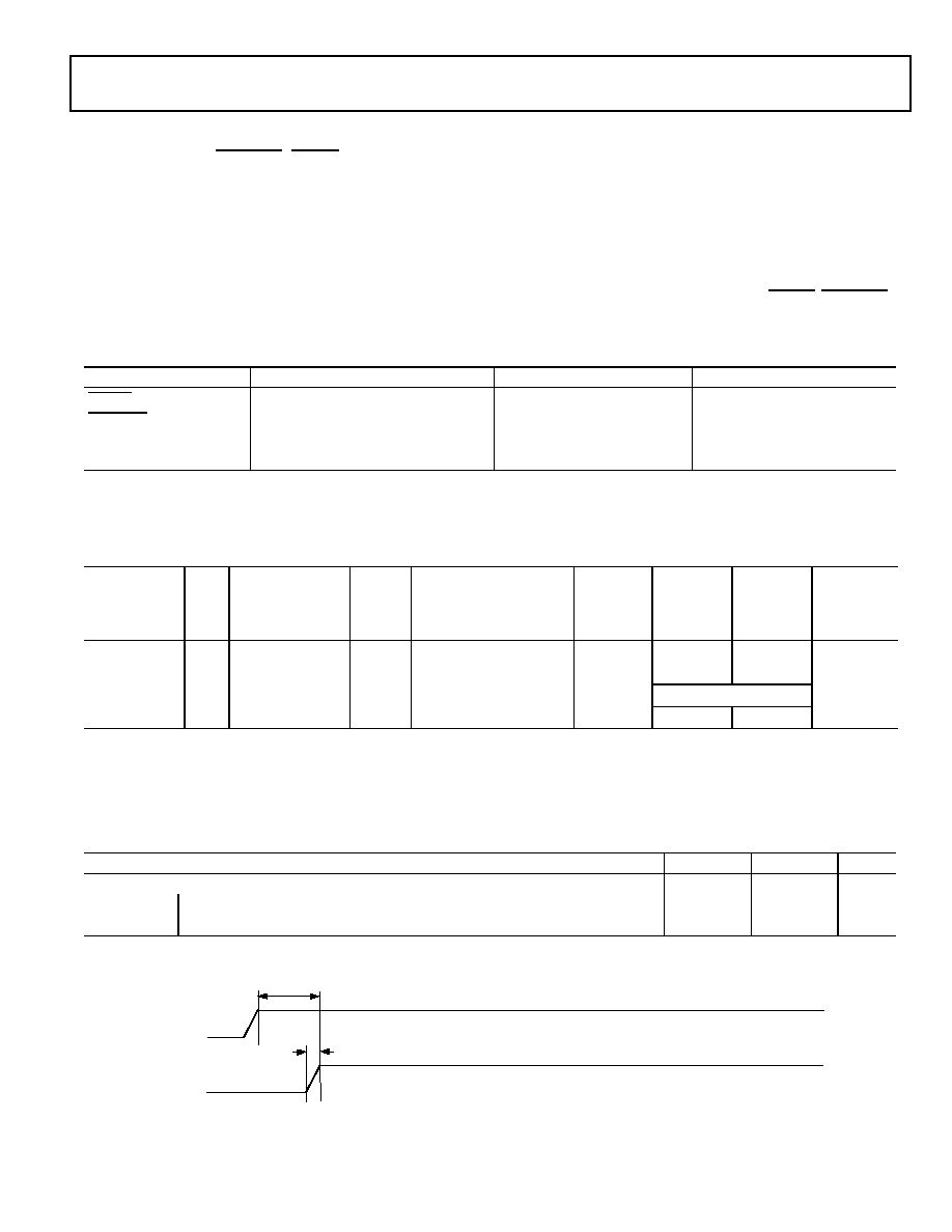
ADSP-TS201S
Preliminary Technical Data
Rev. PrH
|
Page 23 of 40
|
December 2003
TIMING SPECIFICATIONS
With the exception of DMAR30, IRQ30, TMR0E, and
FLAG30 (input only) pins, all AC timing for the ADSP-TS201S
processor is relative to a reference clock edge. Because input
setup/hold, output valid/hold, and output enable/disable times
are relative to a clock edge, the timing data for the ADSP-
TS201S processor has few calculated (formula-based) values.
For information on AC timing, see
General AC Timing on
page 24
. For information on Link port transfer timing, see
Link
Port Low-Voltage, Differential-Signal (LVDS) Electrical Char-
acteristics and Timing on page 28
.
General AC Timing
Timing is measured on signals when they cross the 1.25 V level
as described in
Figure 11 on page 27
. All delays (in nanosec-
onds) are measured between the point that the first signal
reaches 1.25 V and the point that the second signal reaches
1.25 V.
The general AC timing data appears in
Table 18
and
Table 22
.
The AC asynchronous timing data for the IRQ30, DMAR30,
FLAG30, and TMR0E pins appears in
Table 17
.
Table 17. AC Asynchronous Signal Specifications (all values in this table are in nanoseconds)
Name
Description
Pulsewidth Low (min)
Pulsewidth High (min)
IRQ30
1
Interrupt Request
2 × t
SCLK
ns
2 × t
SCLK
ns
DMAR30
1
DMA Request
2 × t
SCLK
ns
2 × t
SCLK
ns
FLAG30
2
FLAG30 Input
2 ×t
SCLK
ns
2× t
SCLK
ns
TMR0E
3
Timer 0 Expired
4 ×t
SCLK
ns
1
These input pins have Schmitt triggers and therefore do not need to be synchronized to a clock reference.
2
For output specifications on FLAG30 pins, see
Table 22
.
3
This pin is a strap option. During reset, an internal resistor pulls the pin low.
Table 18. Reference Clocks
Signal
Type
Description
Speed
Grade
(MHz)
Clock
Cycle
Min (ns)
Clock
Cycle
Max (ns)
Clock
High
Min (ns)
Clock
Low
Min (ns)
Input
Jitter
Tolerance
(ps)
CCLK
1
Core Clock
600
1.67
12.5
500
2.0
12.5
SCLK
2,3,4
I
System Clock
All
Greater of 8 or CCLK×4
50
{40% to 60% Duty Cycle}
100
TCK
I
Test Clock (JTAG)
All
Greater of 30 or CCLK×4
12
12
1
CCLK is the internal DSP clock or instruction cycle time. The period of this clock is equal to the System Clock (SCLK) period divided by the System Clock Ratio (SCLKRAT20).
For information on available part numbers for different internal DSP clock rates, see the
Ordering Guide on page 42
.
2
Actual input jitter should be combined with ac specifications for accurate timing analysis.
3
For more information, see
Table 3 on page 13
.
4
For more information, see Clock Domains on page 9.
Table 19. Power-Up Reset Timing
Parameter
Min
Max
Units
Timing Requirements
t
VDD_DRAM
1
V
DD_DRAM
Stable After V
DD
, V
DD_A
, V
DD_IO
Stable
0
ms
t
VDD_DRAM_RAMP
V
DD_DRAM
Supply Rise Time
0.2
ms
1
Applies only when the internal DRAM regulator is disabled (ENEDREG=0)
Figure 8. Power-Up Timing
V
DD
V
DD_A
V
DD_IO
V
DD_DRAM
t
VDD_DR AM_R AMP
t
VDD_DRAM
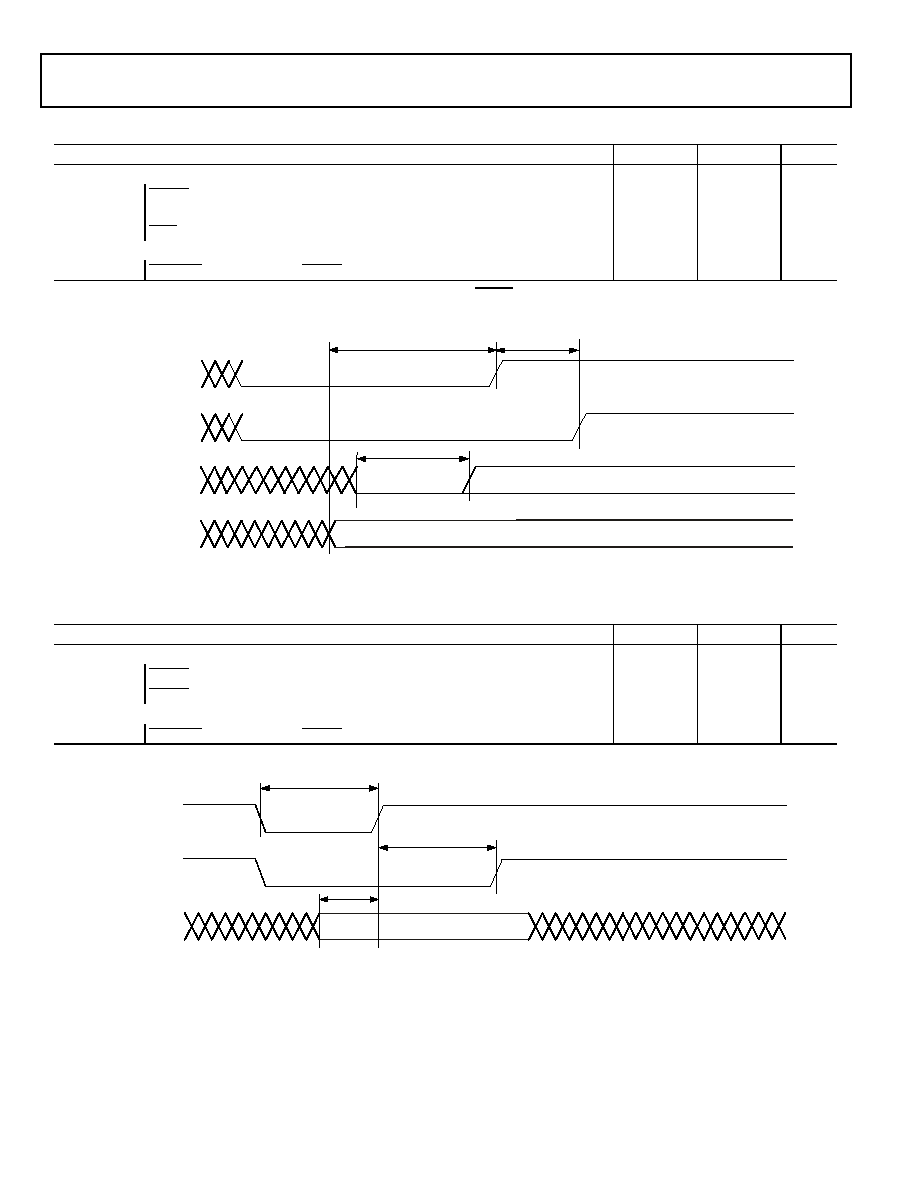
Rev. PrH
|
Page 24 of 40
|
December 2003
ADSP-TS201S
Preliminary Technical Data
Table 20. Power-Up Reset Timing
Parameter
Min
Max
Units
Timing Requirements
t
RST_IN_PWR
RST_IN Deasserted After V
DD
, V
DD_A
, V
DD_IO
, V
DD_DRAM
(ENEDREG=0), SCLK, and
Static/Strap Pins Stable
2
ms
t
TRST_IN_PWR
1
TRST Asserted During Power-Up Reset
100×t
SCLK
ns
Switching Characteristic
t
RST_OUT_PWR
RST_OUT Deasserted After RST_IN Deasserted
1.5
ms
1
Applies after V
DD
, V
DD_A
, V
DD_IO
, V
DD_DRAM
(ENEDREG=0), and SCLK are stable and before RST_IN deasserted.
Figure 9. Power-Up Reset Timing
Table 21. Normal Reset Timing
Parameter
Min
Max
Units
Timing Requirements
t
RST_IN
RST_IN Asserted
2
ms
t
STRAP
RST_IN Deasserted After Strap Pins Stable
1.5
ms
Switching Characteristic
t
RST_OUT
RST_OUT Deasserted After RST_IN Deasserted
1.5
ms
Figure 10. Normal Reset Timing
RST_OUT
t
RST_OUT_PWR
TRST
t
TRST_PWR
SCLK, V
DD,
V
DD_A,
V
DD_IO,
V
DD_DRAM
STATIC/STRAP PINS
RST_IN
t
RST_IN_PWR
STRAP PINS
t
STRAP
RST_IN
t
RST_IN
RST_OUT
t
RST_OUT
ADSP-TS201S
Preliminary Technical Data
Rev. PrH
|
Page 25 of 40
|
December 2003
Table 22. AC Signal Specifications
(all values in this table are in nanoseconds)
Name
Description
In
put S
e
tu
p
(m
i
n
)
In
put Hold
(m
i
n
)
Ou
t
p
u
t
V
a
lid
(m
a
x
)
Ou
t
p
u
t
H
o
ld
(m
i
n
)
Ou
t
p
u
t
En
ab
le
(m
i
n
)
1
Ou
t
p
u
t
Di
sab
l
e
(m
a
x
)
1
Ref
e
r
e
n
c
e
Clock
ADDR310
External Address Bus
1.5
0.5
4.0
1.0
1.15
2.0
SCLK
DATA630
External Data Bus
1.5
0.5
4.0
1.0
1.15
2.0
SCLK
MSH
Memory Select HOST Line
--
--
4.0
1.0
1.15
2.0
SCLK
MSSD30
Memory Select SDRAM Lines
1.5
0.5
4.0
1.0
1.15
2.0
SCLK
MS10
Memory Select for Static Blocks
--
--
4.0
1.0
1.15
2.0
SCLK
RD
Memory Read
1.5
0.5
4.0
1.0
1.15
2.0
SCLK
WRL
Write Low Word
1.5
0.5
4.0
1.0
1.15
2.0
SCLK
WRH
Write High Word
1.5
0.5
4.0
1.0
1.15
2.0
SCLK
ACK
Acknowledge for Data Hi to Low
1.5
0.5
3.6
2.0
1.15
2.0
SCLK
Acknowledge for Data Low to High
1.5
0.5
4.2
2.0
1.15
2.0
SCLK
SDCKE
SDRAM Clock Enable
1.5
0.5
4.0
1.0
1.15
2.0
SCLK
RAS
Row Address Select
1.5
0.5
4.0
1.0
1.15
2.0
SCLK
CAS
Column Address Select
1.5
0.5
4.0
1.0
1.15
2.0
SCLK
SDWE
SDRAM Write Enable
1.5
0.5
4.0
1.0
1.15
2.0
SCLK
LDQM
Low Word SDRAM Data Mask
--
--
4.0
1.0
1.15
2.0
SCLK
HDQM
High Word SDRAM Data Mask
--
--
4.0
1.0
1.15
2.0
SCLK
SDA10
SDRAM ADDR10
--
--
4.0
1.0
1.15
2.0
SCLK
HBR
Host Bus Request
1.5
0.5
--
--
--
--
SCLK
HBG
Host Bus Grant
1.5
0.5
4.0
1.0
1.15
2.0
SCLK
BOFF
Back Off Request
1.5
0.5
--
--
--
--
SCLK
BUSLOCK
Bus Lock
--
--
4.0
1.0
1.15
2.0
SCLK
BRST
Burst pin
1.5
0.5
4.0
1.0
1.15
2.0
SCLK
BR70
Multiprocessing Bus Request pins
1.5
0.5
4.0
1.0
--
--
SCLK
BM
Bus Master Debug aid only
--
--
4.0
1.0
--
--
SCLK
IORD
I/O Read pin
--
--
4.0
1.0
1.15
2.0
SCLK
IOWR
I/O Write pin
--
--
4.0
1.0
1.15
2.0
SCLK
IOEN
I/O Enable pin
--
--
4.0
1.0
1.15
2.0
SCLK
CPA
Core Priority Access Hi to Low
1.5
0.5
4.0
1.0
1.15
2.0
SCLK
Core Priority Access Low to Hi
1.5
0.5
23.5
2.0
1.15
2.0
SCLK
DPA
DMA Priority Access Hi to Low
1.5
0.5
4.0
1.0
1.15
2.0
SCLK
DMA Priority Access Low to Hi
1.5
0.5
23.5
2.0
1.15
2.0
SCLK
BMS
Boot Memory Select
1.5
0.5
4.0
1.0
1.15
2.0
SCLK
FLAG30
2
FLAG pins
--
--
4.0
1.0
1.15
2.0
SCLK
RST_IN
3,4
Global Reset pin
1.5
0.5
--
--
--
--
SCLK
TMS
Test Mode Select (JTAG)
1.5
0.5
--
--
--
--
TCK
TDI
Test Data Input (JTAG)
1.5
0.5
--
--
--
--
TCK
TDO
Test Data Output (JTAG)
--
--
4.0
1.0
1.15
2.0
TCK
TRST
3,4
Test Reset (JTAG)
1.5
0.5
--
--
--
--
TCK
EMU
5
Emulation High to Low
--
--
3.6
2.0
1.15
2.0
TCK or SCLK
ID20
6
Static pins must be constant
--
--
--
--
--
--
--
CONTROLIMP10
6
Static pins must be constant
--
--
--
--
--
--
--
Rev. PrH
|
Page 26 of 40
|
December 2003
ADSP-TS201S
Preliminary Technical Data
DS20
6
Static pins must be constant
--
--
--
--
--
--
--
SCLKRAT20
6
Static pins must be constant
--
--
--
--
--
--
--
ENEDREG
Static pins must be connected to V
SS
--
--
--
--
--
--
--
STRAP SYS
7,8
Strap pins
1.5
0.5
--
--
--
--
SCLK
JTAG SYS
9
JTAG system pins
1.5
0.5
4.0
1.0
--
--
TCK
1
The external port protocols employ bus IDLE cycles for bus mastership transitions as well as slave address boundary crossings to avoid any potential bus contention. The
apparent driver overlap, due to output disables being larger than output enables, is not actual.
2
For input specifications on FLAG30 pins, see
Table 17
.
3
These input pins are asynchronous and therefore do not need to be synchronized to a clock reference.
4
For additional requirement details, see
Reset and Booting on page 9
.
5
Reference clock depends on function.
6
These pins may change only during reset; recommend connecting it to V
DD_IO
/V
SS
.
7
STRAP pins include: BMS, BM, BUSLOCK, TMR0E, L1BCMPO, L2BCMPO, and L3BCMPO.
8
Specifications applicable during reset only.
9
JTAG system pins include: RST_IN, RST_OUT, POR_IN, IRQ3-0, DMAR3-0, HBR, BOFF, MS1-0, MSH, SDCKE, LDQM, HDQM, BMS, IOWR, IORD, BM, EMU, SDA10,
IOEN, BUSLOCK, TMR0E, DATA63-0, ADDR31-0, RD, WRL, WRH, BRST, MSSD3-0, RAS, CAS, SDWE, HBG, BR7-0, FLAG3-0, L0DATOP3-0, L0DATON3-0,
L1DATOP3-0, L1DATON3-0, L2DATOP3-0, L2DATON3-0, L3DATOP3-0, L3DATON3-0, L0CLKOUTP, L0CLKOUTN, L1CLKOUTP, L1CLKOUTN, L2CLKOUTP,
L2CLKOUTN, L3CLKOUTP, L3CLKOUTN, L0ACKI, L1ACKI, L2ACKI, L3ACKI, L0DATIP3-0, L0DATIN3-0, L1DATIP3-0, L1DATIN3-0, L2DATIP3-0, L2DATIN3-0,
L3DATIP3-0, L3DATIN3-0, L0CLKINP, L0CLKINN, L1CLKINP, L1CLKINN, L2CLKINP, L2CLKINN, L3CLKINP, L3CLKINN, L0ACKO, L1ACKO, L2ACKO, L3ACKO,
ACK, CPA, DPA, L0BCMPO, L1BCMPO, L2BCMPO, L3BCMPO, L0BCMPI, L1BCMPI, L2BCMPI, L3BCMPI, ID2-0, CTRL_IMPD1-0, SCLKRAT2-0, DS2-0, ENEDREG.
Figure 11. General AC Parameters Timing
Table 22. AC Signal Specifications (Continued)
(all values in this table are in nanoseconds)
Name
Description
In
put S
e
tu
p
(m
i
n
)
In
put Hold
(m
i
n
)
Ou
t
p
u
t
V
a
lid
(m
a
x
)
Ou
t
p
u
t
H
o
ld
(m
i
n
)
Ou
t
p
u
t
En
ab
le
(m
i
n
)
1
Ou
t
p
u
t
Di
sab
l
e
(m
a
x
)
1
Ref
e
r
e
n
c
e
Clock
REFERENCE
CLOCK
INPUT
SIGNAL
OUTPUT
SIGNAL
THREE-
STATE
OUTPUT
VALID
OUTPUT
HOLD
OUTPUT
ENABLE
OUTPUT
DISABLE
INPUT
HOLD
INPUT
SETUP
1.25V
1.25V
1.25V
t
SCLK
OR
t
TCK
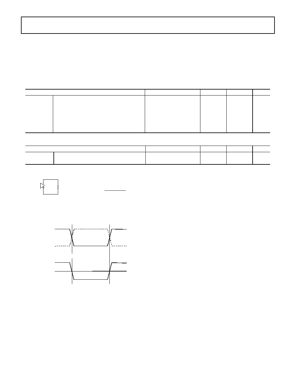
ADSP-TS201S
Preliminary Technical Data
Rev. PrH
|
Page 27 of 40
|
December 2003
Link Port Low-Voltage, Differential-Signal (LVDS)
Electrical Characteristics and Timing
Table 23
and
Table 24
with
Figure 12
provide the electrical
characteristics for the LVDS link ports. The LVDS link port sig-
nal definitions represent all differential signals with a V
OD
= 0 V
level and use signal naming without N (negative) and P (posi-
tive) suffixes (see
Figure 13
).
Table 23. Link Port LVDS Transmit Electrical Characteristics
Parameter
Test Conditions
Min
Max
Units
V
OH
Output Voltage High, V
O_P
or V
O_N
R
L
= 100
1.58
V
V
OL
Output Voltage Low, V
O_P
or V
O_N
R
L
= 100
0.92
V
|V
OD
|
Output Differential Voltage
R
L
= 100
150
450
mV
I
OS
Short-circuit Output Current
V
O_P
or V
O_N
= 0 V
+5/- 40
mA
V
OD
= 0 V
+/- 5
mA
V
OCM
Common Mode Output Voltage
1.13
1.38
V
Table 24. Link Port LVDS Receive Electrical Characteristics
Parameter
Test Conditions
Min
Max
Units
|V
ID
|
Differential Input Voltage
100
600
mV
V
ICM
Common Mode Input Voltage
0.6
1.57
V
Figure 12. Link Ports--Transmit Electrical Characteristics
Figure 13. Link Ports--Signals Definition
VO_N
VO_P
RL
VOCM =
(VO_P + VO_N)
2
VOD = (VO_P VO_N)
Lx<PIN>N
Lx<PI N>P
Lx<PIN>
DIFFERENTIAL PAIR WAVEFO RMS
DIFFERENTIAL VO LTAG E WAVEFORM
VOD = 0V
VO_N
VO_P
VOD = VO_P VO_N
Rev. PrH
|
Page 28 of 40
|
December 2003
ADSP-TS201S
Preliminary Technical Data
Link Port--Data Out Timing
Table 25
with
Figure 14
,
Figure 15
,
Figure 16
,
Figure 17
,
Figure 18
, and
Figure 19
provide the data out timing for the
LVDS link ports.
Table 25. Link Port--Data Out Timing
Parameter
Min
Max
Units
Outputs
t
REO
Rising Edge (
Figure 14
)
200
ps
t
FEO
Falling Edge (
Figure 14
)
200
ps
t
LCLKOP
LxCLKOUT Period (
Figure 15
)
greater of 2.0 or
0.9×LCR×t
CCLK
1,2
1.1×LCR×t
CCLK
1,2
ns
t
LCLKOH
LxCLKOUT High (
Figure 15
0.4×t
LCLKOP
1
0.6×t
LCLKOP
1
ns
t
LCLKOL
LxCLKOUT Low (
Figure 15
)
0.4×t
LCLKOP
1
0.6×t
LCLKOP
1
ns
t
COJT
LxCLKOUT Jitter (
Figure 15
)
/+70
ps
t
LDOS
LxDATO Output Setup, LCR = 1 and LCR = 1.5 (
Figure 16
) smaller of 2.5
3
or
0.25×LCR×t
CCLK
0.15
1,2,4
ns
LxDATO Output Setup, LCR = 2 and LCR = 4 (
Figure 16
)
smaller of 2.5
3
or
0.25×LCR×t
CCLK
0.3
1,2,4
ns
t
LDOH
LxDATO Output Hold, LCR = 1 and LCR = 1.5 (
Figure 16
) 0.25×LCR×t
CCLK
0.15
1,2,4
ns
LxDATO Output Hold, LCR = 2 and LCR = 4 (
Figure 16
)
0.25×LCR×t
CCLK
0.3
1,2,4
ns
t
LACKID
Delay from LxACKI rising edge to first transmission clock
edge (
Figure 17
)
14×LCR×t
CCLK
1,2
ns
t
BCMPOV
LxBCMPO Valid (
Figure 17
)
2×LCR×t
CCLK
1,2
ns
t
BCMPOH
LxBCMPO Hold (
Figure 18
).
3×TSW - 0.5
1,,5
ns
Inputs
t
LACKIS
LxACKI low setup to guarantee that the transmitter stops
transmitting (
Figure 18
).
LxACKI high setup to guarantee that the transmitter
continues its transmission without any interruption
(
Figure 19
).
14×LCR×t
CCLK
1,2
ns
t
LACKIH
LxACKI high hold time (
Figure 18
).
0.5
1
ns
1
Timing is relative to the 0 differential voltage (V
OD
= 0)
2
LCR (Link port Clock Ratio) = 1, 1.5, 2 or 4. t
CCLK
is the core period. Note that LCLK can be a maximum of 500 MHz (for example, if LCR=1 then CCLK must be
500 MHz.).
3
The 2.5 value for t
LDOS
applies for LCLKOUT
100 MHz.
4
t
LDOS
and t
LDOH
values include LCLKOUT jitter.
5
TSW is a short-word transmission period. For a 4-Bit Link it is 2×LCR×t
CCLK
and for a 1-Bit Link is 8×LCR×t
CCLK
ns
Figure 14. Link Ports--Differential Output Signals Transition Time
+
|
VOD
|
MIN
|
VOD
|
MIN
VOD = 0V
t
REO
t
FEO
VO_N
VO_P
RL
CL
CL_P
CL_N
RL = 100
CL = 0.1pF
CL_P = 5pF
CL_N = 5pF
Figure 15. Link Ports--Output Clock
LxCLKOUT
VOD = 0V
t
COJT
t
LCLKOL
t
LCLKOH
t
LCLKOP
ADSP-TS201S
Preliminary Technical Data
Rev. PrH
|
Page 29 of 40
|
December 2003
Figure 16. Link Ports--Data Output Setup and Hold
1
1
These parameters are valid for both clock edges
LxCLKOUT
LxDATO
VOD = 0V
VOD = 0V
t
LDOS
t
LDOH
t
LDOS
t
LDOH
Figure 17. Link Ports--Transmission Start
LxCLKOUT
LxDATO
VOD = 0V
VOD = 0V
t
LACKID
t
BCMPOV
LxACKI
LxBCMPO
Rev. PrH
|
Page 30 of 40
|
December 2003
ADSP-TS201S
Preliminary Technical Data
Figure 18. Link Ports--Transmission End and Stops
Figure 19. Link Ports--Back to Back Transmission
LxCLKOUT
LxDATO
VOD = 0V
VOD = 0V
FIRST EDGE OF 5TH SHORT WORD IN A QUAD WORD
t
LACKIS
t
BCMPOH
LxACKI
LxBCMPO
t
LACKIH
LAST EDGE IN A QUAD WORD
LxCLKOUT
LxDATO
VOD = 0V
VOD = 0V
t
LACKIS
LxACKI
t
LACKIH
LAST EDGE IN A QUAD WORD
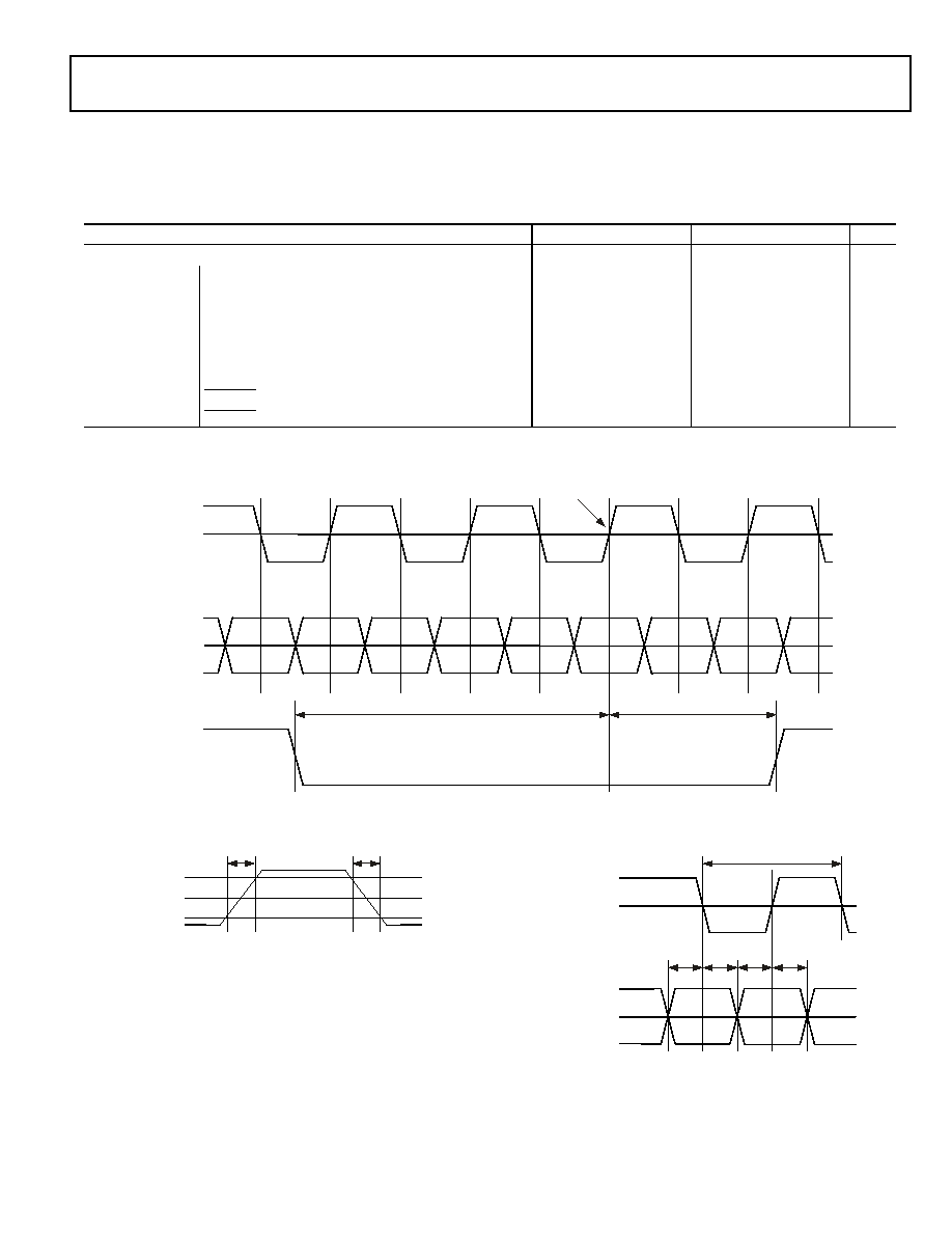
ADSP-TS201S
Preliminary Technical Data
Rev. PrH
|
Page 31 of 40
|
December 2003
Link Port--Data In Timing
Table 26
with
Figure 20
,
Figure 21
, and
Figure 22
provide the
data in timing for the LVDS link ports.
Table 26. Link Port--Data In Timing
Parameter
Min
Max
Units
Inputs
t
LCLKIP
LxCLKIN Period (
Figure 22
)
greater of 1.8 or
0.9×t
CCLK
1
ns
t
REI
Rising Edge (
Figure 21
)
400
ps
t
FEI
Falling Edge (
Figure 21
)
400
ps
t
LDIS
LxDATI Input Setup (
Figure 22
)
0.2
1
ns
t
LDIH
LxDATI Input Hold (
Figure 22
)
0.2
1
ns
t
BCMPIS
LxBCMPI Valid (
Figure 20
)
2×t
LCLKIP
1
ns
t
BCMPIH
LxBCMPI Hold (
Figure 20
)
2×t
LCLKIP
1
ns
1
Timing is relative to the 0 differential voltage (V
OD
= 0)
Figure 20. Link Ports--Last Received Quad Word
LxCLKIN
LxDATI
VOD = 0V
VOD = 0V
t
BCMPIS
LxBCMPI
t
BCMPIH
FIRST EDGE IN FIFTH SHORT WORD IN A QUAD WORD
Figure 21. Link Ports--Differential Input Signals Transition Time
+
|
VOD
|
MIN
|
VOD
|
MIN
VOD = 0V
t
REI
t
FEI
Figure 22. Link Ports--Data Input Setup and Hold
1
1
These parameters are valid for both clock edges
LxCLKIN
LxDATI
VOD = 0V
VOD = 0V
t
LDIS
t
LDIH
t
LDIS
t
LDIH
t
LCLKIP
Rev. PrH
|
Page 32 of 40
|
December 2003
ADSP-TS201S
Preliminary Technical Data
OUTPUT DRIVE CURRENTS
Figure 23
through
Figure 30
show typical IV characteristics for
the output drivers of the ADSP-TS201S processor. The curves in
these diagrams represent the current drive capability of the out-
put drivers as a function of output voltage over the range of
drive strengths. For complete output driver characteristics, refer
to the DSP's IBIS models, available on the Analog Devices web-
site (
www.analog.com
).
Figure 23. Typical Drive Currents at Strength 0
Figure 24. Typical Drive Currents at Strength 1
OUTPUT PIN VOLTAGE V
0
2.8
0.4
0.8
1.2
1.6
2.0
2.4
O
U
T
P
U
T
P
I
N
C
U
R
R
E
N
T
m
A
5
0
5
V
DD_IO
= 2.375V, +85°C
10
15
20
25
30
10
15
20
25
30
STRENGTH 0
V
DD_IO
= 2.5V, +25°C
V
DD_IO
= 2.625V, 40°C
I
OL
I
OH
V
DD_IO
= 2.375V, +85°C
V
DD_IO
= 2.5V, +25°C
V
DD_IO
= 2.625V, 40°C
PR
EL
IM
IN
AR
Y
OUTPUT PIN VOLTAGE V
0
2.8
0.4
0.8
1.2
1.6
2.0
2.4
O
U
T
P
U
T
P
I
N
C
U
R
R
E
N
T
m
A
10
0
10
V
DD_IO
= 2.375V, +85°C
20
30
40
50
70
20
30
40
50
60
STRENGTH 1
V
DD_IO
= 2.5V, +25°C
V
DD_IO
= 2.625V, 40°C
I
OL
I
OH
V
DD_IO
= 2.375V, +85°C
V
DD_IO
= 2.5V, +25°C
V
DD_IO
= 2.625V, 40°C
60
PR
EL
IM
IN
AR
Y
Figure 25. Typical Drive Currents at Strength 2
Figure 26. Typical Drive Currents at Strength 3
Figure 27. Typical Drive Currents at Strength 4
OUTPUT PIN VOLTAGE V
0
2.8
0.4
0.8
1.2
1.6
2.0
2.4
O
U
T
P
U
T
P
I
N
C
U
R
R
E
N
T
m
A
20
0
20
V
DD_IO
= 2.375V, +85°C
40
60
80
100
40
60
80
STRENGTH 2
V
DD_IO
= 2.5V, +25°C
V
DD_IO
= 2.625V, 40°C
I
OL
I
OH
V
DD_IO
= 2.375V, +85°C
V
DD_IO
= 2.5V, +25°C
V
DD_IO
= 2.625V, 40°C
PR
EL
IM
IN
AR
Y
OUTPUT PIN VOLTAGE V
0
2.8
0.4
0.8
1.2
1.6
2.0
2.4
O
U
T
P
U
T
P
I
N
C
U
R
R
E
N
T
m
A
25
0
25
V
DD_IO
= 2.375V, +85°C
50
75
100
125
50
75
100
125
STRENGTH 3
V
DD_IO
= 2.5V, +25°C
V
DD_IO
= 2.625V, 40°C
I
OL
I
OH
V
DD_IO
= 2.375V, +85°C
V
DD_IO
= 2.5V, +25°C
V
DD_IO
= 2.625V, 40°C
PR
EL
IM
IN
AR
Y
OUTPUT PIN VOLTAGE V
0
2.8
0.4
0.8
1.2
1.6
2.0
2.4
O
U
T
P
U
T
P
I
N
C
U
R
R
E
N
T
m
A
20
0
20
V
DD_IO
= 2.375V, +85°C
40
60
80
120
160
40
60
80
120
140
STRENGTH 4
V
DD_IO
= 2.5V, +25°C
V
DD_IO
= 2.625V, 40°C
I
OL
I
OH
V
DD_IO
= 2.375V, +85°C
V
DD_IO
= 2.5V, +25°C
V
DD_IO
= 2.625V, 40°C
100
100
140
PR
EL
IM
IN
AR
Y
ADSP-TS201S
Preliminary Technical Data
Rev. PrH
|
Page 33 of 40
|
December 2003
TEST CONDITIONS
The ac signal specifications (timing parameters) appear
Table 22 on page 26
. These include output disable time, output
enable time, and capacitive loading. The timing specifications
for the DSP apply for the voltage reference levels in
Figure 31
.
Output Disable Time
Output pins are considered to be disabled when they stop driv-
ing, go into a high impedance state, and start to decay from their
output high or low voltage. The time for the voltage on the bus
to decay by
V is dependent on the capacitive load, C
L
and the
load current, I
L
. This decay time can be approximated by the fol-
lowing equation:
The output disable time t
DIS
is the difference between
t
MEASURED_DIS
and t
DECAY
as shown in
Figure 32
. The time
t
MEASURED_DIS
is the interval from when the reference signal
switches to when the output voltage decays
V from the mea-
sured output high or output low voltage. t
DECAY
is calculated
with test loads C
L
and I
L
, and with
V equal to 0.4 V.
Figure 28. Typical Drive Currents at Strength 5
Figure 29. Typical Drive Currents at Strength 6
Figure 30. Typical Drive Currents at Strength 7
OUTPUT PIN VOLTAGE V
0
2.8
0.4
0.8
1.2
1.6
2.0
2.4
O
U
T
P
U
T
P
I
N
C
U
R
R
E
N
T
m
A
20
0
20
V
DD_IO
= 2.375V, +85°C
40
60
80
120
180
40
60
80
120
160
STRENGTH 5
V
DD_IO
= 2.5V, +25°C
V
DD_IO
= 2.625V, 40°C
I
OL
I
OH
V
DD_IO
= 2.375V, +85°C
V
DD_IO
= 2.5V, +25°C
V
DD_IO
= 2.625V, 40°C
140
100
100
160
140
PR
EL
IM
IN
AR
Y
OUTPUT PIN VOLTAGE V
0
2.8
0.4
0.8
1.2
1.6
2.0
2.4
O
U
T
P
U
T
P
I
N
C
U
R
R
E
N
T
m
A
20
0
20
V
DD_IO
= 2.375V, +85°C
40
60
80
100
220
40
60
80
100
180
STRENGTH 6
V
DD_IO
= 2.5V, +25°C
V
DD_IO
= 2.625V, 40°C
I
OL
I
OH
V
DD_IO
= 2.375V, +85°C
V
DD_IO
= 2.5V, +25°C
V
DD_IO
= 2.625V, 40°C
120
140
160
120
140
160
180
200
PR
EL
IM
IN
AR
Y
OUTPUT PIN VOLTAGE V
0
2.8
0.4
0.8
1.2
1.6
2.0
2.4
O
U
T
P
U
T
P
I
N
C
U
R
R
E
N
T
m
A
20
0
20
V
DD_IO
= 2.375V, +85°C
40
60
80
100
220
40
60
80
100
220
STRENGTH 7
V
DD_IO
= 2.5V, +25°C
V
DD_IO
= 2.625V, 40°C
I
OL
I
OH
V
DD_IO
= 2.375V, +85°C
V
DD_IO
= 2.5V, +25°C
V
DD_IO
= 2.625V, 40°C
120
140
160
180
200
120
140
160
180
200
PR
EL
IM
IN
AR
Y
Figure 31. Voltage reference levels for AC measurements (except out-
put enable/disable)
Figure 32. Output Enable/Disable
INPUT
OR
OUTPUT
1.25V
1.25V
t
DECAY
C
L
V
(
)
I
L
/
=
REFERENCE
SIGNAL
t
DIS
OUTPUT STARTS
DRIVING
V
OH (MEASURED)
V
V
OL (MEASURED)
+
V
t
MEASURED_DIS
V
OH (MEASURED)
V
OL (MEASURED)
1.65V
0.85V
HIGH-IMPEDANCE STATE.
TEST CONDITIONS CAUSE THIS
VOLTAGE TO BE APPROXIMATELY 1.25V
OUTPUT STOPS
DRIVING
t
DECAY
t
ENA
t
MEASURED_ENA
t
RAMP
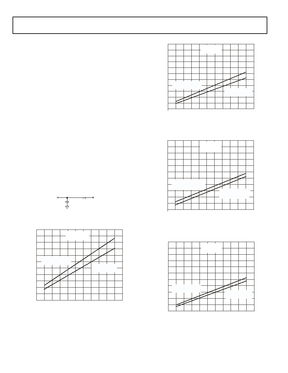
Rev. PrH
|
Page 34 of 40
|
December 2003
ADSP-TS201S
Preliminary Technical Data
Output Enable Time
Output pins are considered to be enabled when they have made
a transition from a high impedance state to when they start driv-
ing. The time for the voltage on the bus to ramp by
V is
dependent on the capacitive load, C
L
, and the drive current, I
D
.
This ramp time can be approximated by the following equation:
The output enable time t
ENA
is the difference between
t
MEASURED_ENA
and t
RAMP
as shown in
Figure 32
. The time
t
MEASURED_ENA
is the interval from when the reference signal
switches to when the output voltage ramps
V from the mea-
sured three-stated output level. t
RAMP
is calculated with test load
C
L
, drive current I
D
, and with
V equal to 0.4 V.
Capacitive Loading
Output valid and hold are based on standard capacitive loads:
30 pF on all pins (see
Figure 33
). The delay and hold specifica-
tions given should be derated by a drive strength related factor
for loads other than the nominal value of 30 pF.
Figure 34
through
Figure 41
show how output rise time varies with capac-
itance.
Figure 42
graphically shows how output valid varies with
load capacitance. (Note that this graph or derating does not
apply to output disable delays; see
Output Disable Time on
page 34
.) The graphs of
Figure 34
through
Figure 42
may not be
linear outside the ranges shown.
Figure 33. Equivalent Device Loading for AC Measurements
(Includes All Fixtures)
Figure 34. Typical Output Rise and Fall Time (10%90%, V
DD_IO
= 2.5 V) vs.
Load Capacitance at Strength 0
t
RAMP
C
L
V
(
)
I
D
/
=
1.25V
TO
OUTPUT
PIN
30pF
50
STRENGTH 0
(V
DD_IO
= 2.5V)
0
10
20
30
40
50
60
70
80
90
100
0
5
10
15
20
25
R
I
S
E
A
N
D
F
A
L
L
T
I
M
E
S
n
s
LOAD CAPACITANCE pF
RISE TIME
y = 0.2015x + 3.8869
FALL TIME
y = 0.174x + 2.6931
PR
EL
IM
IN
AR
Y
Figure 35. Typical Output Rise and Fall Time (10%90%, V
DD_IO
= 2.5 V) vs.
Load Capacitance at Strength 1
Figure 36. Typical Output Rise and Fall Time (10%90%, V
DD_IO
= 2.5 V) vs.
Load Capacitance at Strength 2
Figure 37. Typical Output Rise and Fall Time (10%90%, V
DD_IO
= 2.5 V) vs.
Load Capacitance at Strength 3
0
10
20
30
40
50
60
70
80
90
100
0
5
10
15
20
25
R
I
S
E
A
N
D
F
A
L
L
T
I
M
E
S
n
s
LOAD CAPACITANCE pF
RISE TIME
y = 0.1349x + 1.9955
FALL TIME
y = 0.1163x + 1.4058
STRENGTH 1
(V
DD _IO
= 2.5V)
PR
EL
IM
IN
AR
Y
0
10
20
30
40
50
60
70
80
90
100
0
5
10
15
20
25
R
I
S
E
A
N
D
F
A
L
L
T
I
M
E
S
n
s
LOAD CAPACITANCE pF
RISE TIME
y = 0.1304x + 0.8427
FALL TIME
y = 0.1144x + 0.7025
STRENGTH 2
(V
DD_IO
= 2.5V)
PR
EL
IM
IN
AR
Y
0
10
20
30
40
50
60
70
80
90
100
0
5
10
15
20
25
R
I
S
E
A
N
D
F
A
L
L
T
I
M
E
S
n
s
LOAD CAPACITANCE pF
RISE TIME
y = 0.1082x + 1.3123
FALL TIME
y = 0.0912x + 1.2048
STRENGTH 3
(V
DD_IO
= 2.5V)
PR
EL
IM
IN
AR
Y
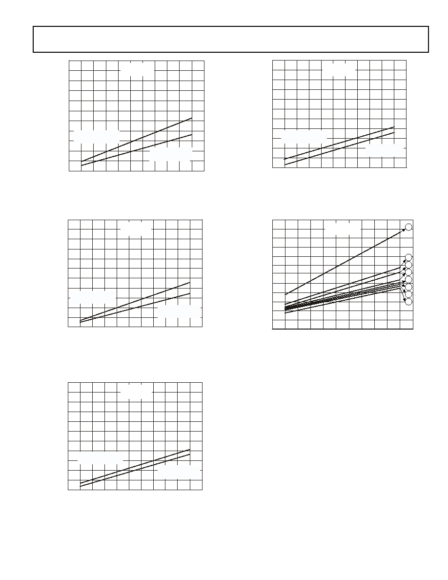
ADSP-TS201S
Preliminary Technical Data
Rev. PrH
|
Page 35 of 40
|
December 2003
Figure 38. Typical Output Rise and Fall Time (10%90%, V
DD_IO
= 2.5 V) vs.
Load Capacitance at Strength 4
Figure 39. Typical Output Rise and Fall Time (10%90%, V
DD_IO
= 2.5 V) vs.
Load Capacitance at Strength 5
Figure 40. Typical Output Rise and Fall Time (10%90%, V
DD_IO
= 2.5 V) vs.
Load Capacitance at Strength 6
0
10
20
30
40
50
60
70
80
90
100
0
5
10
15
20
25
R
I
S
E
A
N
D
F
A
L
L
T
I
M
E
S
n
s
LOAD CAPACITANCE pF
STRENGTH 4
(V
DD _IO
= 2.5V)
RISE TIME
y = 0.1071x + 0.9877
FALL TIME
y = 0.0798x + 1.0743
PR
EL
IM
IN
AR
Y
0
10
20
30
40
50
60
70
80
90
100
0
5
10
15
20
25
R
I
S
E
A
N
D
F
A
L
L
T
I
M
E
S
n
s
LOAD CAPACITANCE pF
RISE TIME
y = 0.1001x + 0.7763
FALL TIME
y = 0.0793x + 0.8691
STRENGTH 5
(V
DD_IO
= 2.5V)
PR
EL
IM
IN
AR
Y
0
10
20
30
40
50
60
70
80
90
100
0
5
10
15
20
25
R
I
S
E
A
N
D
F
A
L
L
T
I
M
E
S
n
s
LOAD CAPACITANCE pF
RISE TIME
y = 0.0946x + 1.2187
FALL TIME
y = 0.0906x + 0.4597
STRENGTH 6
(V
DD_IO
= 2.5V)
PR
EL
IM
IN
AR
Y
Figure 41. Typical Output Rise and Fall Time (10%90%, V
DD_IO
= 2.5 V) vs.
Load Capacitance at Strength 7
Figure 42. Typical Output Valid (V
DD_IO
= 2.5 V) vs. Load Capacitance at Max
Case Temperature and Strength 07
1
1
The line equations for the output valid versus load capacitance are:
Strength 0: y = 0.0956x + 3.5662
Strength 1: y = 0.0523x + 3.2144
Strength 2: y = 0.0433x + 3.1319
Strength 3: y = 0.0391x + 2.9675
Strength 4: y = 0.0393x + 2.7653
Strength 5: y = 0.0373x + 2.6515
Strength 6: y = 0.0379x + 2.1206
Strength 7: y = 0.0399x + 1.9080
0
10
20
30
40
50
60
70
80
90
100
0
5
10
15
20
25
R
I
S
E
A
N
D
F
A
L
L
T
I
M
E
S
n
s
LOAD CAPACITANCE pF
STRENGTH 7
(V
DD_IO
= 2.5V)
RISE TIME
y = 0.0907x + 1.0071
FALL TIME
y = 0.09x + 0.3134
PR
EL
IM
IN
AR
Y
0
10
20
30
40
50
60
70
80
90
100
0
5
10
15
O
U
T
P
U
T
V
A
L
I
D
n
s
LOAD CAPACITANCE pF
STRENGTH 07
(V
DD_IO
= 2.5V)
0
1
2
3
4
5
6
7
PR
EL
IM
IN
AR
Y
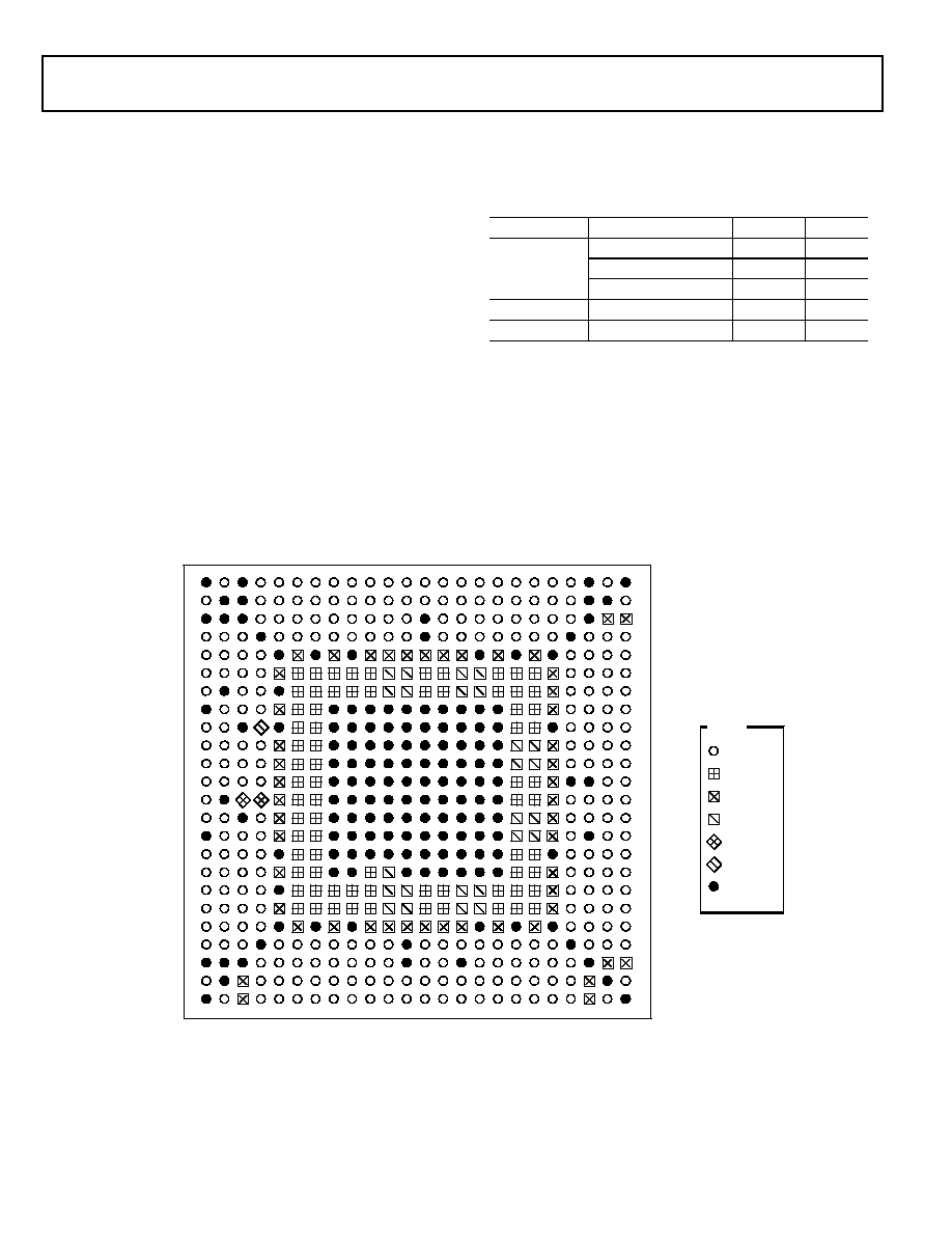
Rev. PrH
|
Page 36 of 40
|
December 2003
ADSP-TS201S
Preliminary Technical Data
ENVIRONMENTAL CONDITIONS
The ADSP-TS201S processor is rated for performance over the
extended commercial temperature range, T
CASE
= 40°C to
85°C.
Thermal Characteristics
The ADSP-TS201S processor is packaged in a 25 mm × 25 mm
thermally enhanced Ball Grid Array (BGA_ED). The ADSP-
TS201S processor is specified for a case temperature (T
CASE
). To
ensure that the T
CASE
data sheet specification is not exceeded, a
heatsink and/or an air flow source may be used.
Table 27
shows the thermal characteristics of the
25 mm × 25 mm BGA_ED package.
576-BALL BGA_ED PIN CONFIGURATIONS
Figure 43
shows a summary of pin configurations for the 576-
ball BGA_ED package and
Table 28
lists the signal-to-ball
assignments.
Table 27. Thermal Characteristics
for 25 mm × 25 mm Package
Parameter
Condition
Typical
Units
JA
Airflow = 0 m/s
19.6
°C/W
Airflow = 1 m/s
15.4
°C/W
Airflow = 2 m/s
13.7
°C/W
JC
0.7
°C/W
JB
8.3
°C/W
Figure 43. 576-ball BGA_ED Pin Configurations
1
(top view, Summary)
1
For a more detailed pin summary diagram, see the EE-179: ADSP-TS201S System Design Guidelines on the Analog Devices website (
www.analog.com
)
TOP VIEW
19
17
21
23
15
13
11
9
5
7
3
1
20
18
16
14
12
10
8
6
2
4
22
24
R
P
N
M
L
K
J
H
G
F
E
D
C
B
A
Y
W
V
U
T
AD
AC
AB
AA
V
DD
V
DD_IO
V
DD_DRAM
V
SS
SIGNAL
V
DD_A
V
REF
KEY:
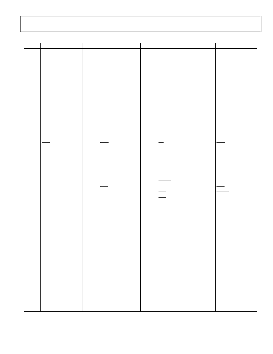
ADSP-TS201S
Preliminary Technical Data
Rev. PrH
|
Page 37 of 40
|
December 2003
Table 28. 576-Ball (25 mm × 25 mm) BGA_ED Pin Assignments
Pin#
Signal Name
Pin#
Signal Name
Pin#
Signal Name
Pin#
Signal Name
A1
V
SS
B1
DATA53
C1
V
SS
D1
DATA55
A2
DATA51
B2
V
SS
C2
V
SS
D2
DATA56
A3
V
SS
B3
V
SS
C3
V
SS
D3
DATA54
A4
DATA49
B4
DATA50
C4
DATA52
D4
V
SS
A5
DATA43
B5
DATA44
C5
DATA47
D5
DATA48
A6
DATA41
B6
DATA42
C6
DATA45
D6
DATA46
A7
DATA37
B7
DATA38
C7
DATA39
D7
DATA40
A8
DATA33
B8
DATA34
C8
DATA35
D8
DATA36
A9
DATA29
B9
DATA30
C9
DATA31
D9
DATA32
A10
DATA25
B10
DATA26
C10
DATA27
D10
DATA28
A11
DATA23
B11
DATA24
C11
DATA21
D11
DATA22
A12
DATA19
B12
DATA20
C12
DATA17
D12
DATA18
A13
DATA15
B13
DATA16
C13
V
SS
D13
V
SS
A14
DATA11
B14
DATA12
C14
DATA13
D14
DATA14
A15
DATA9
B15
DATA10
C15
DATA7
D15
DATA8
A16
DATA5
B16
DATA6
C16
DATA3
D16
DATA4
A17
DATA1
B17
DATA2
C17
ACK
D17
DATA0
A18
WRL
B18
WRH
C18
RD
D18
BRST
A19
ADDR30
B19
ADDR31
C19
ADDR26
D19
ADDR27
A20
ADDR28
B20
ADDR29
C20
ADDR24
D20
ADDR25
A21
ADDR22
B21
ADDR23
C21
ADDR20
D21
V
SS
A22
V
SS
B22
V
SS
C22
V
SS
D22
ADDR19
A23
ADDR21
B23
V
SS
C23
V
DD_IO
D23
ADDR17
A24
V
SS
B24
ADDR18
C24
V
DD_IO
D24
ADDR16
E1
DATA61
F1
DATA63
G1
MSSD1
H1
V
SS
E2
DATA62
F2
MS1
G2
V
SS
H2
MSH
E3
DATA57
F3
DATA59
G3
MS0
H3
MSSD3
E4
DATA58
F4
DATA60
G4
BMS
H4
SCLKRAT0
E5
V
SS
F5
V
DD_IO
G5
V
SS
H5
V
DD_IO
E6
V
DD_IO
F6
V
DD
G6
V
DD
H6
V
DD
E7
V
SS
F7
V
DD
G7
V
DD
H7
V
DD
E8
V
DD_IO
F8
V
DD
G8
V
DD
H8
V
SS
E9
V
SS
F9
V
DD
G9
V
DD
H9
V
SS
E10
V
DD_IO
F10
V
DD
G10
V
DD
H10
V
SS
E11
V
DD_IO
F11
V
DD_DRAM
G11
V
DD_DRAM
H11
V
SS
E12
V
DD_IO
F12
V
DD_DRAM
G12
V
DD_DRAM
H12
V
SS
E13
V
DD_IO
F13
V
DD
G13
V
DD
H13
V
SS
E14
V
DD_IO
F14
V
DD
G14
V
DD
H14
V
SS
E15
V
DD_IO
F15
V
DD_DRAM
G15
V
DD_DRAM
H15
V
SS
E16
V
SS
F16
V
DD_DRAM
G16
V
DD_DRAM
H16
V
SS
E17
V
DD_IO
F17
V
DD
G17
V
DD
H17
V
SS
E18
V
SS
F18
V
DD
G18
V
DD
H18
V
DD
E19
V
DD_IO
F19
V
DD
G19
V
DD
H19
V
DD
E20
V
SS
F20
V
DD_IO
G20
V
DD_IO
H20
V
DD_IO
E21
ADDR15
F21
ADDR13
G21
ADDR7
H21
ADDR3
E22
ADDR14
F22
ADDR12
G22
ADDR6
H22
ADDR2
E23
ADDR11
F23
ADDR9
G23
ADDR5
H23
ADDR1
E24
ADDR10
F24
ADDR8
G24
ADDR4
H24
ADDR0
Rev. PrH
|
Page 38 of 40
|
December 2003
ADSP-TS201S
Preliminary Technical Data
J1
RAS
K1
SDA10
L1
SDWE
M1
BR3
J2
CAS
K2
SDCKE
L2
BR0
M2
SCLKRAT1
J3
V
SS
K3
LDQM
L3
BR1
M3
BR5
J4
V
REF
K4
HDQM
L4
BR2
M4
BR6
J5
V
SS
K5
V
DD_IO
L5
V
DD_IO
M5
V
DD_IO
J6
V
DD
K6
V
DD
L6
V
DD
M6
V
DD
J7
V
DD
K7
V
DD
L7
V
DD
M7
V
DD
J8
V
SS
K8
V
SS
L8
V
SS
M8
V
SS
J9
V
SS
K9
V
SS
L9
V
SS
M9
V
SS
J10
V
SS
K10
V
SS
L10
V
SS
M10
V
SS
J11
V
SS
K11
V
SS
L11
V
SS
M11
V
SS
J12
V
SS
K12
V
SS
L12
V
SS
M12
V
SS
J13
V
SS
K13
V
SS
L13
V
SS
M13
V
SS
J14
V
SS
K14
V
SS
L14
V
SS
M14
V
SS
J15
V
SS
K15
V
SS
L15
V
SS
M15
V
SS
J16
V
SS
K16
V
SS
L16
V
SS
M16
V
SS
J17
V
SS
K17
V
SS
L17
V
SS
M17
V
SS
J18
V
DD
K18
V
DD_DRAM
L18
V
DD_DRAM
M18
V
DD
J19
V
DD
K19
V
DD_DRAM
L19
V
DD_DRAM
M19
V
DD
J20
V
SS
K20
V
DD_IO
L20
V
DD_IO
M20
V
DD_IO
J21
L0ACKO
K21
L0DATI1_N
L21
L0DATI3_N
M21
V
SS
J22
L0BCMPI
K22
L0DATI1_P
L22
L0DATI3_P
M22
V
SS
J23
L0DATI0_N
K23
L0CLKINN
L23
L0DATI2_N
M23
L0DATO3_N
J24
L0DATI0_P
K24
L0CLKINP
L24
L0DATI2_P
M24
L0DATO3_P
N1
ID0
P1
SCLK
R1
V
SS
T1
RST_IN
N2
V
SS
P2
SCLK_VREF
R2
NC (SCLK)
1
T2
SCLKRAT2
N3
V
DD_A
P3
V
SS
R3
NC (SCLK_VREF)
1
T3
BR4
N4
V
DD_A
P4
BM
R4
BR7
T4
DS0
N5
V
DD_IO
P5
V
DD_IO
R5
V
DD_IO
T5
V
SS
N6
V
DD
P6
V
DD
R6
V
DD
T6
V
DD
N7
V
DD
P7
V
DD
R7
V
DD
T7
V
DD
N8
V
SS
P8
V
SS
R8
V
SS
T8
V
SS
N9
V
SS
P9
V
SS
R9
V
SS
T9
V
SS
N10
V
SS
P10
V
SS
R10
V
SS
T10
V
SS
N11
V
SS
P11
V
SS
R11
V
SS
T11
V
SS
N12
V
SS
P12
V
SS
R12
V
SS
T12
V
SS
N13
V
SS
P13
V
SS
R13
V
SS
T13
V
SS
N14
V
SS
P14
V
SS
R14
V
SS
T14
V
SS
N15
V
SS
P15
V
SS
R15
V
SS
T15
V
SS
N16
V
SS
P16
V
SS
R16
V
SS
T16
V
SS
N17
V
SS
P17
V
SS
R17
V
SS
T17
V
SS
N18
V
DD
P18
V
DD_DRAM
R18
V
DD_DRAM
T18
V
DD
N19
V
DD
P19
V
DD_DRAM
R19
V
DD_DRAM
T19
V
DD
N20
V
DD_IO
P20
V
DD_IO
R20
V
DD_IO
T20
V
SS
N21
L0DATO2_N
P21
L0DATO1_N
R21
NC
T21
L1DATI0_N
N22
L0DATO2_P
P22
L0DATO1_P
R22
V
SS
T22
L1DATI0_P
N23
L0CLKON
P23
L0DATO0_N
R23
L0BCMPO
T23
L1ACKO
N24
L0CLKOP
P24
L0DATO0_P
R24
L0ACKI
T24
L1BCMPI
Table 28. 576-Ball (25 mm × 25 mm) BGA_ED Pin Assignments (Continued)
Pin#
Signal Name
Pin#
Signal Name
Pin#
Signal Name
Pin#
Signal Name
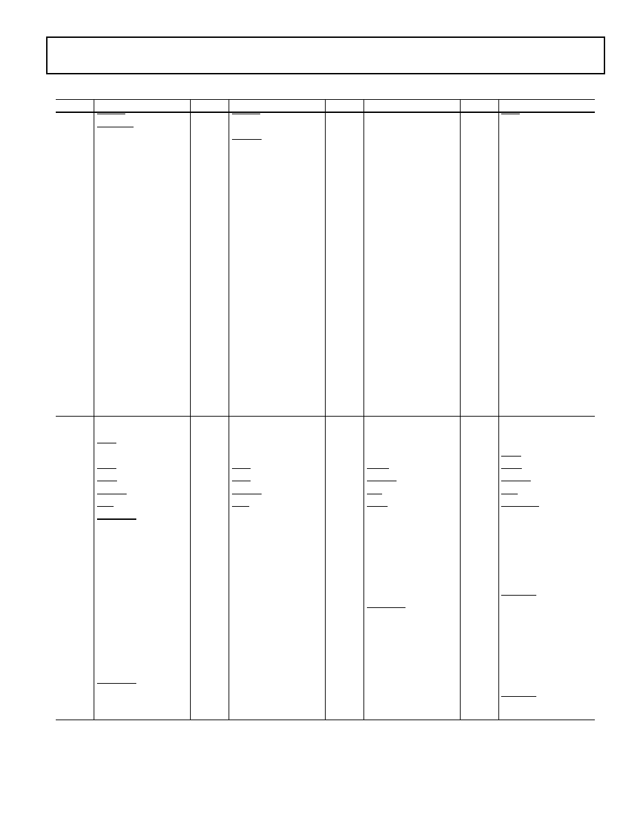
ADSP-TS201S
Preliminary Technical Data
Rev. PrH
|
Page 39 of 40
|
December 2003
U1
MSSD0
V1
MSSD2
W1
CONTROLIMP0
Y1
EMU
U2
RST_OUT
V2
DS2
W2
ENEDREG
Y2
TCK
U3
ID2
V3
POR_IN
W3
TDI
Y3
TMR0E
U4
DS1
V4
CONTROLIMP1
W4
TDO
Y4
FLAG3
U5
V
DD_IO
V5
V
SS
W5
V
DD_IO
Y5
V
SS
U6
V
DD
V6
V
DD
W6
V
DD
Y6
V
DD_IO
U7
V
DD
V7
V
DD
W7
V
DD
Y7
V
SS
U8
V
SS
V8
V
DD
W8
V
DD
Y8
V
DD_IO
U9
V
SS
V9
V
DD
W9
V
DD
Y9
V
SS
U10
V
DD
V10
V
DD
W10
V
DD
Y10
V
DD_IO
U11
V
DD_DRAM
V11
V
DD_DRAM
W11
V
DD_DRAM
Y11
V
DD_IO
U12
V
SS
V12
V
DD_DRAM
W12
V
DD_DRAM
Y12
V
DD_IO
U13
V
SS
V13
V
DD
W13
V
DD
Y13
V
DD_IO
U14
V
SS
V14
V
DD
W14
V
DD
Y14
V
DD_IO
U15
V
SS
V15
V
DD_DRAM
W15
V
DD_DRAM
Y15
V
DD_IO
U16
V
SS
V16
V
DD_DRAM
W16
V
DD_DRAM
Y16
V
SS
U17
V
SS
V17
V
DD
W17
V
DD
Y17
V
DD_IO
U18
V
DD
V18
V
DD
W18
V
DD
Y18
V
SS
U19
V
DD
V19
V
DD
W19
V
DD
Y19
V
DD_IO
U20
V
DD_IO
V20
V
DD_IO
W20
V
DD_IO
Y20
V
SS
U21
L1CLKINN
V21
L1DATI3_N
W21
L1CLKON
Y21
L1DATO1_N
U22
L1CLKINP
V22
L1DATI3_P
W22
L1CLKOP
Y22
L1DATO1_P
U23
L1DATI1_N
V23
L1DATI2_N
W23
L1DATO3_N
Y23
L1DATO2_N
U24
L1DATI1_P
V24
L1DATI2_P
W24
L1DATO3_P
Y24
L1DATO2_P
AA1
FLAG2
AB1
V
SS
AC1
FLAG0
AD1
V
SS
AA2
FLAG1
AB2
V
SS
AC2
V
SS
AD2
ID1
AA3
IRQ3
AB3
V
SS
AC3
V
DD_IO
AD3
V
DD_IO
AA4
V
SS
AB4
NC
AC4
TMS
AD4
TRST
AA5
IRQ0
AB5
IRQ2
AC5
IOWR
AD5
IORD
AA6
IOEN
AB6
IRQ1
AC6
DMAR2
AD6
DMAR3
AA7
DMAR0
AB7
DMAR1
AC7
CPA
AD7
DPA
AA8
HBR
AB8
HBG
AC8
BOFF
AD8
BUSLOCK
AA9
L3BCMPO
AB9
L3ACKI
AC9
L3DATO0_N
AD9
L3DATO0_P
AA10
L3DATO1_N
AB10
L3DATO1_P
AC10
L3CLKON
AD10
L3CLKOP
AA11
L3DATO3_N
AB11
L3DATO3_P
AC11
L3DATO2_N
AD11
L3DATO2_P
AA12
V
SS
AB12
V
SS
AC12
L3DATI3_N
AD12
L3DATI3_P
AA13
L3DATI2_N
AB13
L3DATI2_P
AC13
L3CLKINN
AD13
L3CLKINP
AA14
L3DATI1_N
AB14
L3DATI1_P
AC14
L3DATI0_N
AD14
L3DATI0_P
AA15
NC
AB15
V
SS
AC15
L3ACKO
AD15
L3BCMPI
AA16
L2DATO0_N
AB16
L2DATO0_P
AC16
L2BCMPO
AD16
L2ACKI
AA17
L2CLKON
AB17
L2CLKOP
AC17
L2DATO1_N
AD17
L2DATO1_P
AA18
L2DATO3_N
AB18
L2DATO3_P
AC18
L2DATO2_N
AD18
L2DATO2_P
AA19
L2CLKINN
AB19
L2CLKINP
AC19
L2DATI3_N
AD19
L2DATI3_P
AA20
L2DATI1_N
AB20
L2DATI1_P
AC20
L2DATI2_N
AD20
L2DATI2_P
AA21
V
SS
AB21
L2ACKO
AC21
L2DATI0_N
AD21
L2DATI0_P
AA22
L1BCMPO
AB22
V
SS
AC22
V
DD_IO
AD22
V
DD_IO
AA23
L1DATO0_N
AB23
V
DD_IO
AC23
V
SS
AD23
L2BCMPI
AA24
L1DATO0_P
AB24
V
DD_IO
AC24
L1ACKI
AD24
V
SS
1
On revision 1.x silicon, the R2 and R3 pins are NC. On revision 0.x silicon, the R2 pin is SCLK, and the R3 pin is SCLK_V
REF
. For more information on SCLK and SCLK_V
REF
on revision 0.x silicon, see the EE-179: ADSP-TS20x TigerSHARC System Design Guidelines on the Analog Devices website (
www.analog.com
).
Table 28. 576-Ball (25 mm × 25 mm) BGA_ED Pin Assignments (Continued)
Pin#
Signal Name
Pin#
Signal Name
Pin#
Signal Name
Pin#
Signal Name
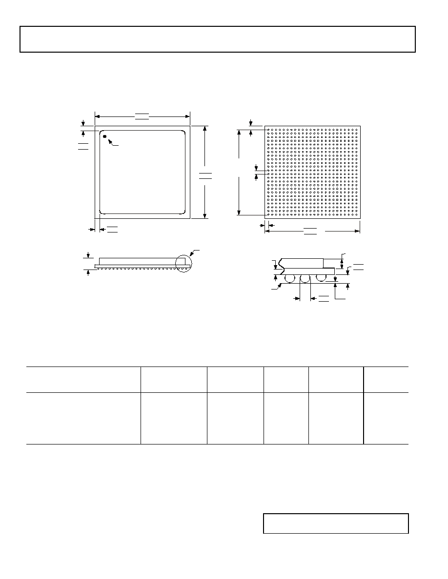
Rev. PrH
|
Page 40 of 40
|
December 2003
ADSP-TS201S
Preliminary Technical Data
© 2003 Analog Devices, Inc. All rights reserved. Trademarks and
registered trademarks are the property of their respective owners.
C00000-0-03/03(0)
www.analog.com
a
OUTLINE DIMENSIONS
The ADSP-TS201S processor is available in a 25 mm × 25 mm,
576-ball metric thermally enhanced Ball Grid Array (BGA_ED) package with 24 rows of balls (BP-576).
ORDERING GUIDE
Figure 44. 576-ball BGA_ED (BP-576)
Part Number
1,2,3,4
1
S indicates 1.0/2.5 V supplies.
2
A indicates 40°C to 85°C temperature.
3
BP indicated thermally enhanced Ball Grid Array (BGA_ED) package.
4
-XX and -X indicate engineering grade products.
Case
Temperature
Range
Instruction
Rate
5
5
The instruction rate is the same as the internal DSP clock (CCLK) rate.
On-chip
DRAM
Operating
Voltage
Package
ADSP-TS201SABP-6X
40°C to 85°C
600 MHz
24Mbit
1.2 V
DD
2.5 V
DD_IO
1.5 V
DD_DRAM
(BP-576)
6
6
The BP-576 package measures 25mm × 25mm.
ADSP-TS201SABP-X
40°C to 85°C
500 MHz
24Mbit
1.0 V
DD
2.5 V
DD_IO
1.5 V
DD_DRAM
(BP-576)
1.00
BSC
SQ
BALL
PITCH
0.75
0.65
0.55
BALL DIAMETER
3.10 MAX
DETAIL A
NOTES:
1. ALL DIMENSIONS ARE IN MILLIMETERS.
2. THE ACTUAL POSITION OF THE BALL GR ID IS WITHIN 0.25mm OF ITS
IDEAL POSITION RELATIVE TO THE PACKAGE EDGES.
3. THE ACTUAL POSITION OF EACH BALL IS WITHIN 0.10mm OF ITS
IDEAL POSITION RELATIVE TO THE BALL GRID.
4. CENTER DIMENSIONS ARE N OMINAL.
5. THIS PACKAGE C ONFORMS WITH TH E JEDEC MS-034 SPECIFICATION.
SEATING PLANE
1.60 MAX
0.20 MAX
DETAIL A
0.97 BSC
25.20
25.00 SQ
24.80
7
9
5
3
1
11
13
15
17
21 19
23
6
8
10
12
14
16
18
20
24 22
4
2
R
P
N
M
L
K
J
H
G
F
E
D
C
B
A
Y
W
V
U
T
AD
AC
AB
AA
23.00
BSC
SQ
25.20
25.00
24.80
25.20
25.00
24.80
TOP VIEW
BOTTOM VIEW
1.00
BSC
0.60
0.50
0.40
1.00
BSC
A1 BALL
INDICATOR
1.25
1.00
0.75
1.25
1.00
0.75
Document Outline