Äîêóìåíòàöèÿ è îïèñàíèÿ www.docs.chipfind.ru

REV. 0
Information furnished by Analog Devices is believed to be accurate and
reliable. However, no responsibility is assumed by Analog Devices for its
use, nor for any infringements of patents or other rights of third parties
which may result from its use. No license is granted by implication or
otherwise under any patent or patent rights of Analog Devices.
a
ADSP-21mod970-110
One Technology Way, P.O. Box 9106, Norwood, MA 02062-9106, U.S.A.
Tel: 781/329-4700
World Wide Web Site: http://www.analog.com
Fax: 781/326-8703
© Analog Devices, Inc., 1999
Multiport Internet
Gateway Processor Solution
FEATURES
High Density
Implements Six Modem Channels in One Package
304-Ball PBGA with a 1.45 Square Inch (961 sq. mm.)
Footprint
ISDN B-Channel HDLC
DATA Modulations
CCITT V.90 (30 kbps56 kbps)
K56FlexTM (30 kbps56 kbps)
ITU-T V.34: 33600 Bits/s2400 Bits/s
CCITT V.32bis: 14400 Bits/s7200 Bits/s
CCITT V.32: 9600 Bits/s, 4800 Bits/s
CCITT V.23
CCITT V.22/V.22bis: 2400, 1200, 600 Bits/s
CCITT V.21: 300 Bits/s
Bell 212A: 1200 Bits/s
Bell 103: 300 Bits/s
Start-Up Procedures:
ITU-T V.8
Error Correction and Data Compression:
CCITT V.42 Error Correction (LAPM and MNP2-4)
CCITT V.42bis Data and MNP Class 5 Compression
FAX Modem
V.17/V.29/V.27ter/V.21 Channel 2
T.30 Protocol
V.120
V.110
PPP Asynchronous Framing Support (RFC 1662)
Low Power
80 mW per Channel Typical Active
Low Power and Sleep Modes
On-Chip DS0/DS1 Interface
Full Function DMA Port
No External Memory Required
3.3 V Supply
Fully Upgradable RAM-Based Architecture
Fast Download
Full Image in 5 ms
High Speed 16-Bit Port Link Bus Provides Simple
Interface Between Host and Modem Pool
K56Flex is a trademark of Rockwell International and Lucent Technologies.
INTRODUCTION
The ADSP-21mod970-110 is a six-channel solution intended
for remote access server and remote access concentrator applica-
tions. It combines a highly integrated DSP processor with
downloadable software. All datapump and controller functions
are implemented on a single 1.45-square-inch chip. This modem
package allows the highest modem port density while achieving
the lowest power consumption in a software upgradable platform.
The ADSP-21mod970-110 is designed for high-density systems
such as remote access servers, see Figure 1. Its high performance
DSP core, large on-chip SRAM, TDM serial port and 16-bit
DMA port provide efficient control and data communication
with minimal chip count. The modem software provides a num-
ber of data modulations, such as V.34, 56 kbps PCM and ISDN
with a software upgrade path to future standards and new appli-
cations, such as voice over network. The host interface allows
system access to modem statistics such as call progress, connect
speed and modulation parameters such as retrain count and
symbol rate.
ON-CHIP SRAM
The ADSP-21mod970-110 processor integrates 960K bytes
of on-chip memory. The modem datapump and controller
software, as well as data storage, are contained in the on-chip
SRAM. The SRAM cells are designed by Analog Devices. These
cells are optimized for high speed digital signal processing and
low power consumption. You can dynamically configure the
ADSP-21mod970-110 with software through the 16-bit DMA
interface.
DMA INTERFACE
The 16-bit internal DMA port (DMA Port) provides transpar-
ent, direct access to the on-chip RAM of the ADSP-21mod970-110
processor. This high speed access to on-chip memory simpli-
fies control and data communication and system debug. Use the
16-bit DMA interface to dynamically configure the ADSP-
21mod970-110 with software.
REV. 0
ADSP-21mod970-110
2
DMA
ADSP-21mod970
SP0
LAN
OR
INTERNET
T1
E1
PRI
xDSL
ATM
DMA
ADSP-21mod970
SP0
DMA
ADSP-21mod970
SP0
DMA
ADSP-21mod970
SP0
DMA
ADSP-21mod970
SP0
DMA
ADSP-21mod970
SP0
PORT LINK
BUS
DMA
ADSP-21mod970
SP0
DMA
ADSP-21mod970
SP0
HOST
ADSP-2183
ADSP-21mod970 FUNCTIONS
V.34/56k MODEM
V.17 FAX
V.42, V.42bis, MNP2-5
DTMF DIALING
CALLER ID
HDLC PROTOCOL
HOST FUNCTIONS
MULTI-DSP CONTROL, OVERLAY MANAGEMENT
AND DATA TRANSFERS
FRAMER
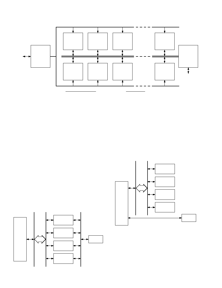
Figure 1. ADSP-21mod970 Network Access System
SERIAL PORTS
The ADSP-21mod970-110 processor incorporates two complete
synchronous, double-buffered serial ports for serial communica-
tions. The serial ports interface directly to a time-division
multiplexed (TDM) 1544 kbps (T1) or 2048 kbps (E1) serial
stream, to an 8K sample/s data stream, or to an 8-bit companded
(64 kb/s) data stream (DS0). The serial ports operate under
modem software control.
SUPPORTED SYSTEM ARCHITECTURES
The ADSP-21mod970-110 Multiport Internet Gateway Proces-
sor supports two system architectures: serial Telco PCM TDM
data stream and parallel Telco PCM data stream. The two archi-
tectures are differentiated by the method of proving Telco PCM
data to the DSP Modem.
Serial Telco PCM TDM Data Stream Architecture
The serial Telco PCM TDM data stream architecture, shown in
Figure 2, is the most common architecture. In this architecture,
the modem pool may have a local Telco interface that provides
a serial TDM data stream of Telco PCM data to the DSP through
the DSP's Serial Port. You can connect up to 24/32 DSPs,
through the Serial Port, to a 24-/32-channel serial TDM data
stream.
ADSP-21mod970
ADSP-21mod970
ADSP-21mod970
ADSP-21mod970
TELCO PCM
I/F
HOST
MEMORY
I/F
DMA
PORT
SERIAL
PORT
Figure 2. Serial Telco PCM TDM Data Stream Architecture
Parallel Telco PCM Data Stream Architecture
The parallel Telco PCM data stream architecture, shown in
Figure 3, provides a single bus interface for all data and control.
In this architecture, the modem pool may have a remote Telco
interface that provides a parallel data stream of Telco PCM data
to the DSP through the DSP's DMA Port. An arbitrary number
of DSPs can be connected, through the DMA Port, to a Host
that provides the parallel data stream.
Note: The number of parallel DSPs is limited only by the soft-
ware loading constraints on the Host.
ADSP-21mod970
ADSP-21mod970
ADSP-21mod970
ADSP-21mod970
TELCO PCM
I/F
HOST
MEMORY
I/F
DMA
PORT
Figure 3. Parallel Telco PCM Data Stream Architecture
REV. 0
ADSP-21mod970-110
3
SOFTWARE INTERFACE
Analog Devices provides sample C code for the software inter-
face to the ADSP-21mod970-110. The software interface en-
compasses the following four areas--download, control interface,
data interface and modem statistics.
Download
The DMA Port on the ADSP-21mod970-110 contains an auto-
incrementing address generator. The host writes the starting
address of the transfer and then writes the first word of data.
After the first write, the DMA address generator automatically
increments; the host writes the next data word and the DMA
transfers that word to the next location in ADSP-21mod970-
110 memory.
The executable image contains code and data that must be
loaded into program and data memory. Program memory on the
ADSP-21mod970-110 is 24 bits wide, therefore two transfers
are used to load each word of program memory.
The host begins the download by asserting the
RESET pin of
the ADSP-21mod970-110. The host then transfers all code and
data. All internal memory can be loaded in 5 ms.
Control Interface
The ADSP-21mod970-110 is controlled through two FIFOs in
DSP memory. The host sends a control event by writing to the
host-to-modem FIFO. The ADSP-21mod970-110 posts events to
the host by writing into the modem-to-host FIFO.
Data Interface
All data transferred to and from the ADSP-21mod970-110
passes through word FIFOs located in internal memory on the
ADSP-21mod970-110. The FIFOs are accessed through a
control structure that contains a pointer to the start of the FIFO
in memory, the length of the FIFO in 16-bit words, a pointer to
the next address to be read, and a pointer to the next address to
be written. The transmit and receive FIFOs are 1024 bytes
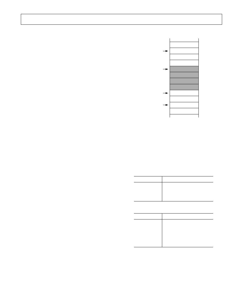
deep. Example code providing primitives for accessing the byte-
FIFOs is available from Analog Devices. Table I shows an ex-
ample of a data FIFO.
Table I. FIFO Example
INFO
INFO
INFO
INFO
BASE
PD_PTR
WR_PDR
BASE + SIZE
Modem Statistics
Several modem statistics can be gathered through the DMA
Port. These statistics include call status, modulation in use,
connect rate, transmit and receive data rate, symbol rate, retrain
count, rate renegotiation count and others. Table II and Table IV
contain a complete listing of available modem statistics.
Modem Configuration
The modem is configured by programming various parameters
through the DMA Port. Table III and Table V contain complete
lists of modem configuration parameters.
Table II. Shell Status
Reference #
Function
SS. 0
Product Number
SS. 1
Application Version
SS. 2
Application Type
SS. 3
Programmable Flag Data
Table III. Shell Parameters
Reference #
Function
SP. 0
Serial Port Tx Time Slot
SP. 1
Serial Port Rx Time Slot
SP. 2
Serial Port Configuration
SP. 3
Programmable Flag Control
SP. 4
Programmable Flag Data
SP. 5
Host Interrupt Count

REV. 0
ADSP-21mod970-110
4
Table IV. Modem Status
Reference #
Function
MS. 0
Data Modulation State
MS. 1
SNR MSE Measure
MS. 2
Rx Level dBm
MS. 3
Tx Level dBm
MS. 4
Tx V.34 Symbol Rate
MS. 5
Rx V.34 Symbol Rate
MS. 6
Round Trip Delay
MS. 7
Telemetry Data Update
MS. 8
Constellation X
MS. 9
Constellation Y
MS. 10
Variable 2 X Pointer
MS. 11
Variable 2 Y Pointer
MS. 12
Variable 3 X Pointer
MS. 13
Variable 3 Y Pointer
MS. 14
Variable 4 X Pointer
MS. 15
Variable 4 Y Pointer
MS. 16
Data Modulation Monitor Retrain Local Count
MS. 17
Data Modulation Monitor Retrain Remote Count
MS. 18
Data Modulation Monitor Retrain Auto Count
MS. 19
Data Modulation Monitor Renegotiate Local
Count
MS. 20
Data Modulation Monitor Renegotiate Remote
Count
MS. 21
Data Modulation Monitor Renegotiate Auto
Count
MS. 22
Omc Carrier Family
MS. 23
Omc Disconnect Reason
MS. 24
Omc State
MS. 25
Omc Time
MS. 26
Omc Idle Time Start
MS. 27
Omc Data Protocol Time Start
MS. 28
Omc Initial Rx Data Rate
MS. 29
Omc Current Rx Data Rate
MS. 30
Omc Initial Tx Data Rate
MS. 31
Omc Current Tx Data Rate
MS. 32
Data Protocol
MS. 33
Data Protocol Compression
MS. 34
Data Protocol Rx HDLC Error Frame Count
MS. 35
Data Protocol Rx HDLC Frame Count
MS. 36
Data Protocol Tx HDLC Frame Count
MS. 37
Data Protocol Tx Data Frame Count
MS. 38
Data Protocol Tx Data Frame Retransmit Count
MS. 39
Data Protocol Rx Data Frame Count
MS. 40
Data Protocol Rx Data Frame Missing Count
MS. 41
Data Modulation Monitor Retrain Remote
Count
MS. 42
Data Protocol Call Tx Data Compressibility
Metric
MS. 43
Data Protocol Call Rx Data Compressibility
Metric
MS. 44
Data Protocol Call Tx Data Metric
MS. 45
Data Protocol Call Rx Data Metric
MS. 46
V.PCM Digital Attenuation
MS. 47
V.PCM Robbed Bit Mask
MS. 48
V.PCM Coding Law
Table V. Modem Parameters
Reference #
Function
MP. 0
Omc Data Modulation Originate Enable
MP. 1
Dial Billing Delay Duration
MP. 2
Omc Data Modulation/Data Protocol
Maximum Start-Up Duration
MP. 3
Data Protocol Start Delay
MP. 4
Data Protocol Allowed Mask
MP. 5
Data Protocol Preferred Mask
MP. 6
Data Protocol Auto-Select Mask
MP. 7
Data Protocol Compression Mask
MP. 8
Data Protocol Cmn Binary Enable
MP. 9
Data Protocol Cmn HDLC Enable
MP. 10
Data Protocol LAPM to Sync
MP. 11
Data Protocol MNP Block Mode Enable
MP. 12
Data Protocol MNP Data Compression Select
MP. 13
Data Protocol MNP Header Optimize Enable
MP. 14
Data Protocol MNP Maximum Data Size
MP. 15
Data Protocol MNP Service Class
MP. 16
Data Protocol Disconnect Management Mode
MP. 17
Data Protocol Disconnect Management
Duration
MP. 18
Digital Data Modes
MP. 19
Pump Data Modes
MP. 20
Pump Tone Transmit Level
MP. 21
Pump Transmit Level
MP. 22
Pump V.34 Transmit Level
MP. 23
Data Modulation Carrier Detect Duration
MP. 24
Data Modulation Carrier Loss Disconnect
Timer Duration
MP. 25
Data Modulation Line Quality Monitor Mode
MP. 26
Data Modulation Options Mask
MP. 27
Data Modulation V.32 Rate Enable Mask
MP. 28
Data Modulation V.34 Data Rate Mask
MP. 29
V.PCM Maximum Power
MP. 30
V.PCM Reference Point
MP. 31
K56 RBS Maximum
MP. 32
K56 Tx Data Rate Maximum
MP. 33
K56 Tx Data Rate Minimum
MP. 34
DTE Interface Big Endian
MP. 35
PPP Rx Mode Enable
MP. 36
PPP Tx Mode Enable
MP. 37
f
P
PPP Detect Enable
MP. 38
f
P
PPP Rx ACCM
MP. 39
f
P
PPP Tx ACCM

REV. 0
ADSP-21mod970-110
5
ORDERING GUIDE
Package
Part Number
Description
Processor Clock
Package Description
Option
ADSP-21mod970-110 with
312 MIPS DSP with Modem
Unit Software License
Software Unit License
26.0 MHz
304 Plastic Ball Grid Array
BP-304
RELATED DOCUMENTS
For further information see the ADSP-21mod970 Multiport Internet Gateway Processor data sheet.
ESD SENSITIVITY
ESD (electrostatic discharge) sensitive device. Electrostatic charges as high as 4000 V readily
accumulate on the human body and test equipment and can discharge without detection. Although
the ADSP-21mod970-110 features proprietary ESD protection circuitry, permanent damage may
occur on devices subjected to high energy electrostatic discharges. Therefore, proper ESD precau-
tions are recommended to avoid performance degradation or loss of functionality.
WARNING!
ESD SENSITIVE DEVICE
REV. 0
ADSP-21mod970-110
6
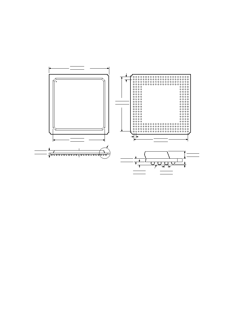
OUTLINE DIMENSIONS
Dimensions shown in inches and (mm).
C349325/99
PRINTED IN U.S.A.
304-Plastic Ball Grid Array
(BP-304)
0.048 (1.22)
0.046 (1.17)
0.044 (1.12)
SEATING
PLANE
0.008 (0.20)
MAX
DETAIL A
0.035 (0.90)
0.030 (0.75)
0.024 (0.60)
BALL DIAMETER
0.024 (0.62)
0.022 (0.56)
0.020 (0.50)
0.028 (0.70)
0.024 (0.60)
0.020 (0.50)
DETAIL A
0.100 (2.54)
0.092 (2.33)
0.083 (2.12)
1.224 (31.10)
1.220 (31.00) SQ
1.217 (30.90)
1.051 (26.70)
1.037 (26.35) SQ
1.024 (26.00)
TOP VIEW
0.050 (1.27)
BSC
1.104 (28.04)
1.100 (27.94)
1.096 (27.84)
0.050 (1.27)
BSC
BOTTOM VIEW
A
B
C
D
E
F
G
H
J
K
L
M
N
P
R
T
U
V
W
Y
AA
AB
AC
23 22 21 20 19 18 17 16 15 14 13 12 11 10 9 8 7 6 5 4 3 2 1
NOTE
THE ACTUAL POSITION OF THE BALL POPULATION IS WITHIN 0.011 (0.30)
OF ITS IDEAL POSITION RELATIVE TO THE PACKAGE EDGES. THE
ACTUAL POSITION OF EACH BALL IS WITHIN 0.004 (0.10) OF ITS IDEAL
POSITION RELATIVE TO THE BALL POPULATION.
1.104 (28.04)
1.100 (27.94)
1.096 (27.84)