ADSP-21mod970 Data Sheet
Information furnished by Analog Devices is believed to be accurate and
reliable. However, no responsibility is assumed by Analog Devices for its
use, nor for any infringements of patents or other rights of third parties
which may result from its use. No license is granted by implication or
otherwise under any patent or patent rights of Analog Devices.
a
ADSP-21mod970
One Technology Way, P.O. Box 9106, Norwood, MA 02062-9106, U.S.A.
Tel: 781/329-4700
World Wide Web Site: http://www.analog.com
Fax: 781/326-8703
© Analog Devices, Inc., 1999
REV. 0
Multiport Internet
Gateway Processor
FUNCTIONAL BLOCK DIAGRAM
16
16
4
16
16
9
4
4
6
6
66
6
6
6
6
6
6
55
27
DATA<23:8>
CLKIN
IAD<15:0>
IDMA CNTL
SPORT0A
SPORT1
EMULATOR
DATA<23:8>_1
CLKIN_1,
BUS CNTL_1
4
4
8
IAD<15:0>_1
DT1<5:0>
TFS0<5:0>
IS
<5:0>
EE<5:0>
CLKOUT<5:0>
RESET
<5:0>
FLAGS
BGH
<5:0>
BG
<5:0>
6
BR
<5:0>
SPORT0B
V
DD
GROUND
MODEM
CHANNEL
2
MODEM
CHANNEL
3
MODEM
CHANNEL
4
MODEM
CHANNEL
5
MODEM
CHANNEL
6
MODEM
CHANNEL
1
IDMA CNTL =
IAL
,
IRD
,
IWR
,
IACK
FLAGS = FL<0:2>, PF<0:7>
BUS CNTL = A0,
BMS
,
PMS
,
DMS
,
CMS
,
IOMS
,
RD
,
WR
EMULATOR =
EMS
, EINT, ELIN,
EBR
,
EBG
, ECLK,
ELOUT,
ERESET
SPORT0A, SPORT0B = RFS0, DR0, DT0, SCLK0
SPORT1 = RFS1, DR1, SCLK1, TFS1
ADSP-21mod970
IDMA CNTL_1
FEATURES
PERFORMANCE
Complete Single-Chip Multiport Internet Gateway
Processor (No External Memory Required)
Implements Six Modem Channels in One Package
Each Processor Can Implement V.34/V.90 Data/Fax
Modem (Includes Datapump and Controller)
312 MIPS Sustained Performance, 19 ns Instruction Time
@ 3.3 V
Open Architecture Extensible to Voice Over IP and Other
Applications
Low Power Dissipation, 100 mW (Typical) per Digital
Modem Processor
Power-Down Mode Featuring Low CMOS Standby
Power Dissipation
INTEGRATION
ADSP-2100 Family Code Compatible, with Instruction
Set Extensions
960K Bytes of On-Chip RAM, Configured as 576K Bytes
of Program Memory and 384K Bytes of Data Memory
Dual Purpose Program Memory for Both Instruction
and Data Storage
304-Ball PBGA with a 1.45 Square Inch (961 sq. mm)
Footprint
GENERAL DESCRIPTION
The ADSP-21mod970 is a Multiport Internet Gateway Pro-
cessor optimized for implementation of a complete V.34/56K
modem. All data pump and controller functions can be imple-
mented on a single device, offering the lowest power consump-
tion and highest possible modem port density.
The ADSP-21mod970 combines the ADSP-2100 family base
architecture (three computational units, data address generators
and a program sequencer) with two serial ports, a 16-bit internal
DMA port, a byte DMA port, a programmable timer, Flag I/O,
extensive interrupt capabilities and on-chip program and data
memory.
The ADSP-21mod970 integrates 960 bytes of on-chip memory,
configured as 192K words (24-bit) of program RAM, and 192K
words (16-bit) of data RAM. Power-down circuitry is also
provided to meet the low power needs of battery operated por-
table equipment. The ADSP-21mod970 is available in a
31 sq-mm., 304-lead PBGA package.
SYSTEM CONFIGURATION
16-Bit Internal DMA Port for High Speed Access to On-
Chip Memory (Mode Selectable)
Programmable Multichannel Serial Port Supports
24 Channels/32 Channels
Two Double-Buffered Serial Ports with Companding
Hardware and Automatic Data Buffering
Separate RESET Pins for Each Internal Processor

ADSP-21mod970
2
REV. 0
Fabricated in a high speed, low power, CMOS process, the
ADSP-21mod970 operates with a 19 ns instruction cycle time.
Every instruction can execute in a single processor cycle.
The ADSP-21mod970's flexible architecture and comprehen-
sive instruction set allow the processor to perform multiple
operations in parallel. In one processor cycle, the ADSP-
21mod970 can:
· Generate the next program address
· Fetch the next instruction
· Perform one or two data moves
· Update one or two data address pointers
· Perform a computational operation
This takes place while the processor continues to:
· Receive and transmit data through the two serial ports
· Receive and/or transmit data through the internal DMA port
· Receive and/or transmit data through the byte DMA port
· Decrement timer
Modem Software
The modem software executes general modem control, com-
mand sets, error correction and data compression, data
modulations (for example, V.90 and V.34), and host interface
functions. The host interface allows system access to modem
statistics such as call progress, connect speed, retrain count,
symbol rate and other modulation parameters.
The modem data pump and controller software reside in on-
chip SRAM and do not require additional memory. The user
can configure the ADSP-21mod970 dynamically by download-
ing software from the host through the 16-bit DMA interface.
This SRAM-based architecture provides a software upgrade
path to future standards and applications, such as voice over IP.
The modem software is available as object code.
DEVELOPMENT SYSTEM
The ADSP-2100 Family Development Software, a complete set
of tools for software and hardware system development, supports
the ADSP-21mod970. The System Builder provides a high level
method for defining the architecture of systems under develop-
ment. The Assembler has an algebraic syntax that is easy to
program and debug. The Linker combines object files into an
executable file. The Simulator provides an interactive instruction-
level simulation with a reconfigurable user interface to display
different portions of the hardware environment.
A PROM Splitter generates PROM programmer compatible
files. The C Compiler, based on the Free Software Foundation's
GNU C Compiler, generates ADSP-21mod970 assembly source
code. The source code debugger allows programs to be cor-
rected in the C environment. The Runtime Library includes
over 100 ANSI-standard mathematical and DSP-specific
functions.
The ADSP-218x EZ-ICE
®
Emulator aids in the hardware de-
bugging of an ADSP-21mod970 system. The EZ-ICE, in con-
junction with the required processor selection hardware, lets you
independently debug code on individual modem processors.
The emulator consists of hardware, host computer resident
software, and the target board connector. The ADSP-21mod970
integrates on-chip emulation support with a 14-pin ICE-PortTM
interface. The ADSP-21mod970 device need not be removed
from the target system when using the EZ-ICE, nor are any
adapters needed. Due to the small footprint of the EZ-ICE
connector, emulation can be supported in final board designs.
The EZ-ICE performs a full range of functions, including:
· In-target operation
· Up to 20 breakpoints
· Single-step or full-speed operation
· Registers and memory values can be examined and altered
· PC upload and download functions
· Instruction-level emulation of program booting and execution
· Complete assembly and disassembly of instructions
· C source-level debugging
See "Designing An EZ-ICE-Compatible Target System" in the
ADSP-2100 Family EZ-Tools Manual (ADSP-2181 sections) as
well as the Designing an EZ-ICE Compatible System section of
this data sheet for the exact specifications of the EZ-ICE target
board connector.
Additional Information
This data sheet provides a general overview of ADSP-21mod970
functionality. For specific information about the modem proces-
sors, refer to the ADSP-21mod870 data sheet. For additional
information on the architecture and instruction set of the mo-
dem processors, refer to the ADSP-2100 Family User's Manual,
Third Edition. For more information about the development
tools, refer to the ADSP-2100 Family Development Tools Data
Sheet.
EZ-ICE is a registered trademark of Analog Devices, Inc.
ICE-Port is a trademark of Analog Devices, Inc.
ADSP-21mod970
3
REV. 0
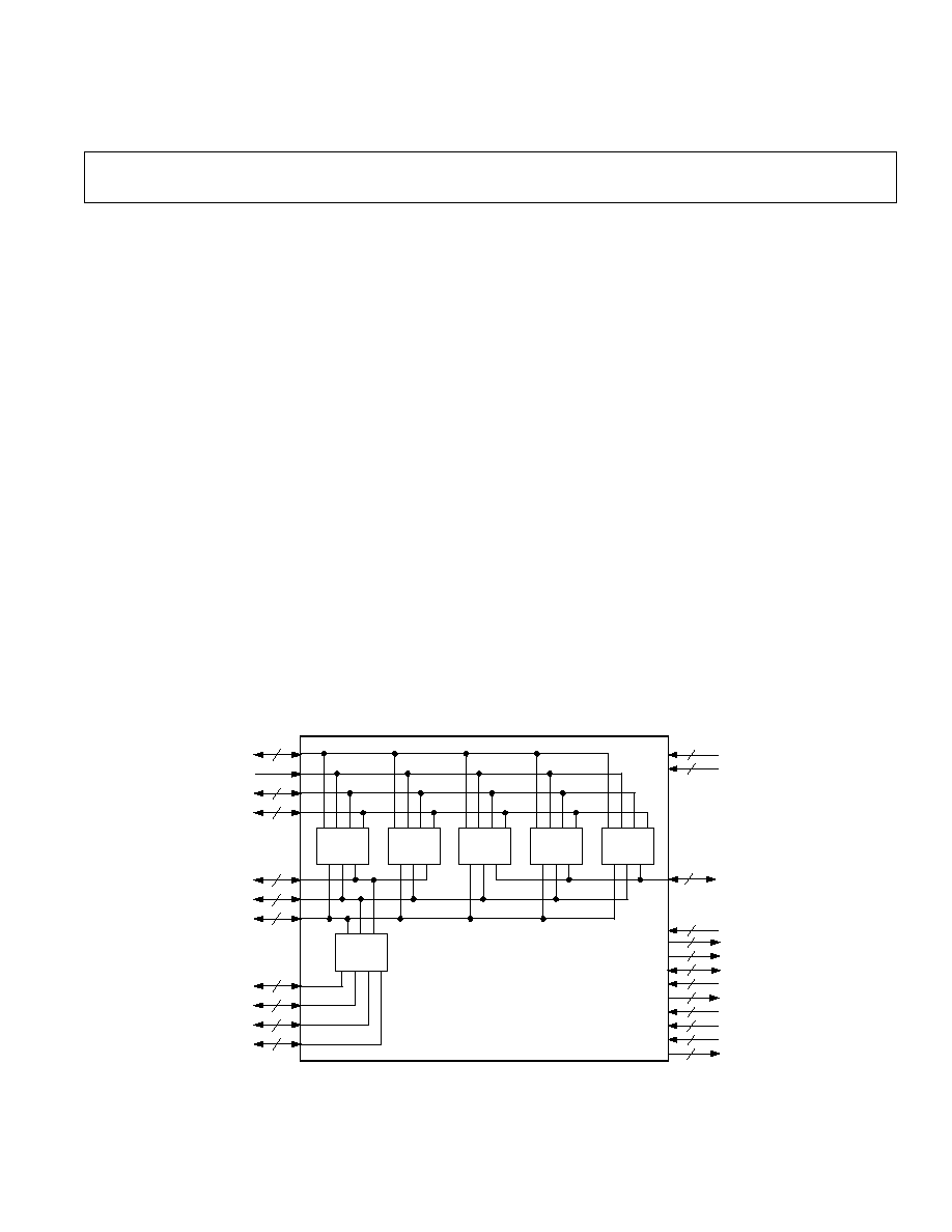
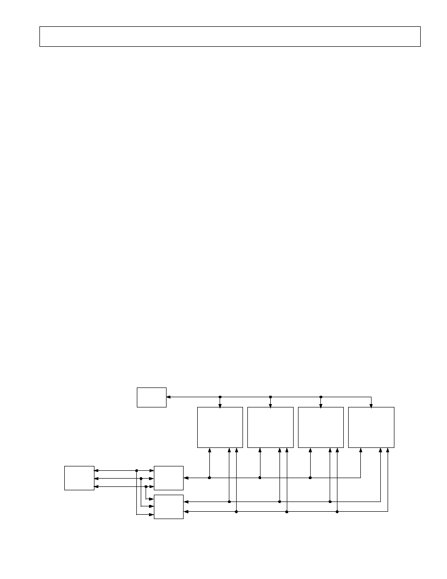
ARCHITECTURE OVERVIEW
Figure 1 is an overall block diagram of the ADSP-21mod970
modem pool. The modem pool contains six independent digital
modem processors.
Each individual modem processor has a DSP core, 160K bytes
of RAM, two serial ports, and a DMA port. The signals for a
single processor are shown in Figure 2. The signals of each
modem processor are accessed through the external pins of the
ADSP-21mod970. Some signals are bused with the signals of
the other processors and are accessed through a single external
pin. Other signals remain separate and they are accessed through
separate external pins for each processor.
The arrangement of the six modem processors in the ADSP-
21mod970 makes two basic configurations possible: a master
configuration and a slave configuration. In both configurations,
the control and data pins of five of the six processors connect to
a single bus structure. The control and data pins of the one
modem processor (Modem Processor 1) are separate from the
other modem processors and accessed through external pins.
In Slave Mode, all six modem processors have identical func-
tions and have equal status. Each modem processor is con-
nected to a common DMA bus and each modem processor is
configured to operate in the same mode (see the Slave Mode
and the Memory Mode descriptions in the Memory Architecture
16
16
4
16
16
9
4
4
55
27
DATA<23:8>
CLKIN
IAD<15:0>
IDMA CNTL
SPORT0A
SPORT1
EMULATOR
DATA<23:8>
CLKIN_1,
BUS CNTL
4
4
8
IAD<15:0>
IDMA CNTL
DT1<5:0>
TFS0<5:0>
IS
<5:0>
EE<5:0>
CLKOUT<5:0>
RESET
<5:0>
FLAGS
BGH
<5:0>
BG
<5:0>
BR
<5:0>
SPORT0B
V
DD
GND
MODEM
CHANNEL
2
MODEM
CHANNEL
3
MODEM
CHANNEL
4
MODEM
CHANNEL
5
MODEM
CHANNEL
6
MODEM
CHANNEL
1
IDMA CNTL =
IAL
,
IRD
,
IWR
,
IACK
FLAGS = FL<0:2>, PF<0:7>
BUS CNTL = A0,
BMS
,
PMS
,
DMS
,
CMS
,
IOMS
,
RD
,
WR
EMULATOR =
EMS
, EINT, ELIN,
EBR
,
EBG
, ECLK, ELOUT,
ERESET
SPORT0A, SPORT0B = RFS0, DR0, DT0, SCLK0
SPORT1 = RFS1, DR1, SCLK1, TFS1
ADSP-21mod970
6
6
66
6
6
6
6
6
6
6
THE FOLLOWING SIGNALS ARE ROUTED TO EACH ADSP-21mod970:
NOTES:
IRQ FUNCTIONS ARE MULTIPLEXED
WITH PROGRAMMABLE FLAGS
(SEE ADSP-21mod870 DATA SHEET)
Figure 1. Modem Pool
PF7/
IRQ
2
PF6/
IRQ
1
PF5/
IRQ
0
PF4/
IRQ
E
PF3/MODE D
PF2/MODE C
PF1/MODE B
PF0/MODE A
FL2
FL1
FL0
EE
IS
TFS0
DT1
BGH
BG
BR
CLKOUT
RESET
A0
BMS
PMS
DMS
CMS
IOMS
RD
WR
DATA 23:8
IAD 15:0
IAL
IRD
IRW
IACK
DATA 23:8
IAD 15:0
IAL
IRD
IRW
IACK
EMS
EINT
ELIN
EBR
EBG
ECLK
ELOUT
RFS0
DR0
DT0
SCLK0
RFS1
DR1
TFS1
MODEM PROCESSOR
ERESET
SCLK1
CLKIN
INDIVDUAL
SIGNALS
BUSED
SIGNALS
MODEM
PROCESSOR 1
MODEM
PROCESSOR 1
(ONLY)
Figure 2. Modem Processor Signals
ADSP-21mod970
4
REV. 0
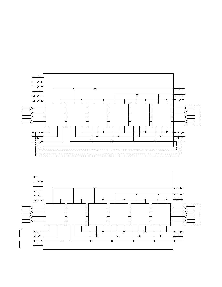
section). The Slave Mode is considered to be the normal mode
of operation in a modem pool application. Figure 3 shows the
modem pool configured for slave mode operation.
The master mode of the ADSP-21mod970 configures five of the
modem processors with identical functions and isolates one of
the modem processors, Processor 1. In the Master Mode, Pro-
cessor 1 is not connected to the DMA bus as are the other five
modem processors. Processor 1 operates in a different mode
where external pins can be used for access to a 16-bit data bus,
a 14-bit address bus with associated bus control pins. In master
FLAGS
IDMA
DATA &
CONTROL BUS
21
24
ADSP-21mod970
HIGH/1
MODE A
MODE A
MODE B
MODE B
MODE C
MODE C
MODE D
MODE D
5
HIGH/1
HIGH/1
HIGH/1
LOW/0
CLKIN
25
16
IDMA
DATA BUS
CLKIN
BGH
BG
BR
RESET
CLKOUT
4
SPORT0A
SPORT0B
ICE
14
4
SPORT0A BUS
SPORT0B BUS
ICE BUS
SPORT0
ICE
IDMA
D&CB
MODEM
PROCESSOR
6
(SLAVE)
SPORT0
ICE
IDMA
D&CB
MODEM
PROCESSOR
5
(SLAVE)
SPORT0
ICE
IDMA
D&CB
MODEM
PROCESSOR
4
(SLAVE)
SPORT0
ICE
IDMA
D&CB
MODEM
PROCESSOR
3
(SLAVE)
SPORT0
ICE
IDMA
D&CB
MODEM
PROCESSOR
2
(SLAVE)
SPORT0
ICE
MODEM
PROCESSOR
1
(MASTER)
ADDR
CNTL
HIGH/1
HIGH/1
LOW/0
42
6
6
6
6
6
Figure 3. Configured for Slave Mode
CONTROL
ADDRESS
DATA
CLKIN
42
FLAGS
7
ADSP-21mod970
HIGH/1
MODE A
MODE A
MODE B
MODE B
MODE C
MODE C
MODE D
MODE D
5
HIGH/1
HIGH/1
HIGH/1
LOW/0
25
16
IDMA
DATA BUS
CLKIN
BGH
BG
BR
RESET
CLKOUT
6
6
6
6
6
4
SPORT0A
SPORT0B
ICE
14
4
SPORT0A BUS
SPORT0B BUS
ICE BUS
SPORT0
ICE
IDMA
D&CB
MODEM
PROCESSOR
6
(SLAVE)
SPORT0
ICE
IDMA
D&CB
MODEM
PROCESSOR
5
(SLAVE)
SPORT0
ICE
IDMA
D&CB
MODEM
PROCESSOR
4
(SLAVE)
SPORT0
ICE
IDMA
D&CB
MODEM
PROCESSOR
3
(SLAVE)
SPORT0
ICE
IDMA
D&CB
MODEM
PROCESSOR
2
(SLAVE)
SPORT0
ICE
MODEM
PROCESSOR
1
(MASTER)
ADDR
CNTL
HIGH/1
HIGH/1
LOW/0
14
24
MASTER
Figure 4. Configured for Master Mode
mode, Processor 1 is treated as a master of the modem pool and
communicates with an external device such as a RAM, ROM or
a memory shared with a host processor. In this configuration,
the master processor performs some controlling function of the
remaining five modem processors. Figure 4 shows the modem
pool configured for Slave Mode operation.
Since the memory bus of Processor 1 is accessible via external
pins in master mode, Processor 1 can be configured for one of
the several memory modes available on the ADSP-21xx family.
(See Full Memory, Host Mode Descriptions.)
ADSP-21mod970
5
REV. 0
Serial Ports
The ADSP-21mod970 has a multichannel serial port (SPORT)
connected to each internal digital modem processor for serial
communications.
Following is a brief list of the capabilities of the ADSP-21mod970
SPORT. For additional information on the internal Serial Ports,
refer to the ADSP-2100 Family User's Manual, Third Edition.
·
SPORT is bidirectional and has a separate, double-buffered
transmit and receive section.
·
SPORT can use an external serial clock or generate its own
serial clock internally.
·
SPORT has independent framing for the receive and trans-
mit sections. Sections run in a frameless mode or with frame
synchronization signals internally or externally generated.
Frame sync signals are active high or inverted, with either of
two pulsewidths and timings.
·
SPORT supports serial data word lengths from 3 to 16 bits
and provides optional A-law and
µ
-law companding accord-
ing to CCITT recommendation G.711.
·
SPORT receive and transmit sections can generate unique
interrupts on completing a data word transfer.
·
SPORT can receive and transmit an entire circular buffer of
data with one overhead cycle per data word. An interrupt is
generated after a data buffer transfer.
·
A multichannel interface selectively receives and transmits a
24- or 32-word, time-division multiplexed, serial bitstream.
PIN DESCRIPTIONS
The ADSP-21mod970 is available in a 304-lead PBGA package.
In order to maintain maximum functionality and reduce pack-
age size and pin count, some serial port, programmable flag,
interrupt and external bus pins have dual, multiplexed function-
ality. The external bus pins are configured during RESET only,
while serial port pins are software configurable during program
execution. Flag and interrupt functionality is retained concur-
rently on multiplexed pins. In cases where pin functionality is
reconfigurable, the default state is shown in plain text; alternate
functionality is shown in italics.
Common-Mode Pins
#
Input/
Pin
of
Out-
Name(s)
Pins put
Function
RESET
6
I
Processor Reset Input
BR
6
I
Bus Request Input
BG
6
O
Bus Grant Output
BGH
6
O
Bus Grant Hang Output
DMS
1
O
Data Memory Select Output
PMS
1
O
Program Memory Select Output
BMS
1
O
Byte Memory Select Output
IOMS
I
O
I/O Memory Select Output
CMS
1
O
Combined Memory Select Output
RD
1
O
Memory Read Enable Output
WR
1
O
Memory Write Enable Output
IRQ2/
6
I
Edge- or Level-Sensitive Interrupt
Request
1
PF7
I/O
Programmable I/O Pin
IRQL1/
6
I
Level-Sensitive Interrupt Requests
1
PF6
I/O
Programmable I/O Pin
IRQL0/
6
I
Level-Sensitive Interrupt Requests
1
PF5
I/O
Programmable I/O Pin
IRQE/
6
I
Edge-Sensitive Interrupt Requests
1
PF4
I/O
Programmable I/O Pin
Mode D/
6
I
Mode Select Input--Checked Only
During RESET
PF3
I/O
Programmable I/O Pin During
Normal Operation
Mode C/
6
I
Mode Select Input--Checked Only
During RESET
PF2
I/O
Programmable I/O Pin During
Normal Operation
Mode B/
6
I
Mode Select Input--Checked Only
During RESET
PF1
I/O
Programmable I/O Pin During
Normal Operation
Mode A/
6
I
Mode Select Input--Checked Only
During RESET
PF0
I/O
Programmable I/O Pin During
Normal Operation
CLKIN
2
I
Clock Input
CLKOUT
6
O
Processor Clock Output
SPORT
24
I/O
Serial Port I/O Pins
2
FL0, FL1, FL2
18
O
Output Flags
V
DD
and GND
82
I
Power and Ground
EZ-Port
14
I/O
For Emulation Use
NOTES
1
Interrupt/Flag Pins retain both functions concurrently. If IMASK is set to
enable the corresponding interrupts, the modem pool will vector to the appro-
priate interrupt vector address when the pin is asserted, either by external
devices, or set as a programmable flag.
2
SPORT configuration determined by the modem pool's System Control Regis-
ter. Software configurable.

ADSP-21mod970
6
REV. 0
Memory Interface Pins
The ADSP-21mod970 modem pool can be used in one of two
modes, master mode or slave mode. In master mode, Modem
Processor 1 operates with full memory (BDMA operation with
full external overlay memory and I/O capability). In Slave Mode,
Modem Processor 1 operates in host configuration (IDMA
operation with limited external addressing capabilities). The
operating mode is determined by the state of the Mode C pin
during RESET and cannot be changed while the modem pool
is running. See the Memory Architecture section for more
information.
Full Memory Pins (Mode C = 0) Modem Processor 1 Only
#
Pin
of
Input/
Name
Pins Output Function
A13:0
14
O
Address Output Pins for Program,
Data, Byte and I/O Spaces
D23:0
24
I/O
Data I/O Pins for Program, Data,
Byte and I/O Spaces (8 MSBs Are
Also Used as Byte Memory Addresses)
Host Pins (Mode C = 1)*
Modem Processor 1 and Modem Processors 26
#
Pin
of
Input/
Name
Pins Output Function
IAD15:0 32
I/O
IDMA Port Address/Data Bus
A0
1
O
Address Pin for External I/O, Pro-
gram, Data, or Byte Access (Modem
Processor 1 Only)
D23:8
32
I/O
Data I/O Pins for Program, Data
Byte and I/O Spaces
IWR
2
I
IDMA Write Enable
IRD
2
I
IDMA Read Enable
IAL
2
I
IDMA Address Latch Pin
IS
6
I
IDMA Select
IACK
2
O
IDMA Port Acknowledge Config-
urable in Mode D; Open Drain
*In Host Mode, external peripheral addresses can be decoded using the A0,
CMS, PMS, DMS, BMS and IOMS signals of Modem Processor 1.
Interrupts
The interrupt controller allows each modem processor in the
modem pool to respond individually to eleven possible inter-
rupts and reset with minimum overhead. The ADSP-21mod970
provides four dedicated external interrupt input pins, IRQ2,
IRQL1, IRQL0, and IRQE (shared with the PF7:4 pins) for
each modem processor. The ADSP-21mod970 also supports
internal interrupts from the timer, the byte DMA port, the serial
port, software and the power-down control circuit. The inter-
rupt levels are internally prioritized and individually maskable
(except power-down and reset). The IRQ2, IRQL1, and IRQL0
input pins can be programmed to be either level- or edge-sensitive.
IRQL0 and IRQL1 are level-sensitive and IRQE is edge sensi-
tive. The priorities and vector addresses of all interrupts are
shown in Table I.
Table I. Interrupt Priority and Interrupt Vector Addresses
Interrupt Vector
Source Of Interrupt
Address (Hex)
RESET (or Power-Up with PUCR = 1) 0000 (Highest Priority)
Power-Down (Nonmaskable)
002C
IRQ2
0004
IRQL1
0008
IRQL0
000C
SPORT0 Transmit
0010
SPORT0 Receive
0014
IRQE
0018
BDMA Interrupt
001C
SPORT1 Transmit or IRQ1
0020
SPORT1 Receive or IRQ0
0024
Timer
0028 (Lowest Priority)
When the modem pool is reset, interrupt servicing is disabled.
LOW POWER OPERATION
The ADSP-21mod970 has three low power modes that signifi-
cantly reduce the power dissipation when the device operates
under standby conditions. These modes are:
· Power-Down
· Idle
· Slow Idle
The CLKOUT pin may also be disabled to reduce external
power dissipation.
Power-Down
The ADSP-21mod970 modem pool has a low power feature
that lets the modem pool enter a very low power dormant state
through software control. Following is a brief list of power-down
features. Refer to the ADSP-2100 Family User's Manual, Third
Edition, "System Interface" chapter, for detailed information
about the power-down feature.
·
Quick recovery from power-down. The modem pool begins
executing instructions in as few as 400 CLKIN cycles.
·
Support for an externally generated TTL or CMOS proces-
sor clock. The external clock can continue running during
power-down without affecting the lowest power rating and 400
CLKIN cycle recovery.
·
Power-down is initiated by the software power-down force
bit. Interrupt support allows an unlimited number of instruc-
tions to be executed before optionally powering down. The
power-down interrupt also can be used as a nonmaskable,
edge-sensitive interrupt.
·
Context clear/save control allows the modem pool to con-
tinue where it left off or start with a clean context when leav-
ing the power-down state.
·
The RESET pin also can be used to terminate power-down.
Idle
When the ADSP-21mod970 is in the idle mode, the modem
pool waits indefinitely in a low power state until an interrupt
occurs. When an unmasked interrupt occurs, it is serviced;
execution then continues with the instruction following the
IDLE instruction. In idle mode IDMA, BDMA and autobuffer
cycle steals still occur.
ADSP-21mod970
7
REV. 0
Slow Idle
The IDLE instruction is enhanced on the ADSP-21mod970 to
let the modem pool's internal clock signal be slowed, further
reducing power consumption. The reduced clock frequency, a
programmable fraction of the normal clock rate, is specified by a
selectable divisor given in the IDLE instruction.
The format of the instruction is
IDLE (n);
where n = 16, 32, 64 or 128. This instruction keeps the modem
pool fully functional, but operating at the slower clock rate.
While it is in this state, the modem pool's other internal clock
signals, such as SCLK, CLKOUT and timer clock, are reduced
by the same ratio. The default form of the instruction, when no
clock divisor is given, is the standard IDLE instruction.
When the IDLE (n) instruction is used, it effectively slows down
the modem pool's internal clock and thus its response time to
incoming interrupts. The one-cycle response time of the stan-
dard idle state is increased by n, the clock divisor. When an
enabled interrupt is received, the ADSP-21mod970 will remain
in the idle state for up to a maximum of n modem pool cycles
(n = 16, 32, 64 or 128) before resuming normal operation.
When the IDLE (n) instruction is used in systems that have an
externally generated serial clock (SCLK), the serial clock rate
may be faster than the modem pool's reduced internal clock
rate. Under these conditions, interrupts must not be generated
at a faster rate than can be serviced, due to the additional time
the modem pool takes to come out of the idle state (a maximum
of n cycles).
SYSTEM CONFIGURATION
Figure 5 shows a typical multichannel modem configuration
with the ADSP-21mod970. A line interface can be used to
connect the multichannel subscriber or client data stream to the
multichannel serial port of the ADSP-21mod970. The ADSP-
21mod970 can support up to 64 channels. The IDMA port of
the ADSP-21mod970 is used to give a host processor full access
to the internal memory of the ADSP-21mod970. This lets the
host dynamically configure the ADSP-21mod970 by loading code
and data into its internal memory. This configuration also lets
SPORT
IDMA
ST/CNTL
T1/E1
LINE
INTERFACE
HOST
MICRO
HOST CONTROL
HOST ADDRESS
HOST DATA
STATUS
&
CONTROL
PAL
IDMA
PAL
IDMA CONTROL
IDMA ADDRESS
STATUS
& CONTROL
ADSP-21mod970
(SLAVE MODE)
SPORT
IDMA
ST/CNTL
ADSP-21mod970
(SLAVE MODE)
SPORT
IDMA
ST/CNTL
ADSP-21mod970
(SLAVE MODE)
SPORT
IDMA
ST/CNTL
ADSP-21mod970
(SLAVE MODE)
Figure 5. Multichannel Modem Configuration
the host access server data directly from the ADSP-21mod970's
internal memory. In this configuration, the Modem Processor 1
should be put into host memory mode where Mode D = 1,
Mode C = 1, Mode B = 0, and Mode A = 1 (see Table II).
CLOCK SIGNALS
The ADSP-21mod970 is clocked by a TTL-compatible clock
signal that runs at half the instruction rate; a 26 MHz input clock
yields a 19 ns processor cycle (which is equivalent to 52 MHz).
Normally, instructions are executed in a single processor cycle.
All device timing is relative to the internal instruction clock
rate, which is indicated by the CLKOUT signal when enabled.
The clock input signal is connected to the processor's CLKIN
input.
The CLKIN input cannot be halted, changed during operation,
or operated below the specified frequency during normal opera-
tion. The only exception is while the processor is in the power-
down state. For additional information, refer to Chapter 9,
ADSP-2100 Family User's Manual, Third Edition, for a detailed
explanation of this power-down feature.
A clock output (CLKOUT) signal is generated by the processor
at the processor's cycle rate.
Reset
The RESET signals initiate a reset of each modem processor in
the ADSP-21mod970. The RESET signals must be asserted
during the power-up sequence to assure proper initialization.
RESET during initial power-up must be held long enough to
let the internal clocks stabilize. If RESETs are activated any
time after power-up, the clocks continue to run and do not
require stabilization time.
The power-up sequence is defined as the total time required for
the oscillator circuits to stabilize after a valid V
DD
is applied to
the processors, and for the internal phase-locked loops (PLL)
to lock onto the specific frequency. A minimum of 2000 CLKIN
cycles ensures that the PLLs have locked, but this does not
include the oscillators start-up time. During this power-up
sequence, the RESET signals should be held low. On any sub-
sequent resets, the RESET signals must meet the minimum
pulsewidth specification, t
RSP
.
ADSP-21mod970
8
REV. 0
The RESET inputs contain some hysteresis; however, if an RC
circuit is used to generate the RESET signals, the use of external
Schmidt triggers are recommended.
The reset for each individual modem processor sets the internal
stack pointers to the empty stack condition, masks all interrupts
and clears the MSTAT register. When a RESET is released, if
there is no pending bus request and the modem processor is
configured for booting, the boot-loading sequence is performed.
The first instruction is fetched from on-chip program memory
location 0x0000 once boot loading completes.
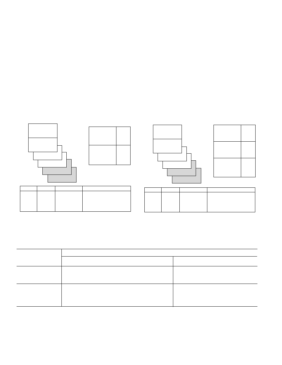
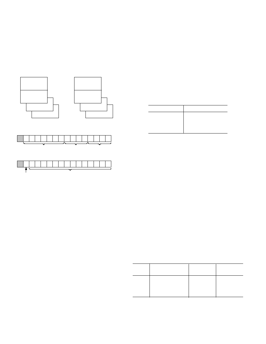
MEMORY ARCHITECTURE
The ADSP-21mod970 provides a variety of memory and pe-
ripheral interface options for Modem Processor 1. The key
functional groups are Program Memory, Data Memory, Byte
Table II. Processor and Memory Mode
Memory Modes
ADSP-21mod970 Modes
for
Modem Processor 1
Master
Slave
Host
· All Internal Program Memory Available
· All Internal Program Memory Available
· All Internal Data Memory Available
· All Internal Data Memory Available
· IDMA Port Enabled
· IDMA Port Enabled
Full-Memory
· All Internal and External Program Memory Available
Not Applicable
· All Internal and External Data Memory Available
· I/O Space Available
· Byte Memory DMA (BDMA) Enabled
Memory and I/O. Refer to the figures and tables below for PM
and DM memory allocations in the ADSP-21mod970.
The ADSP-21mod970 modem pool operates in one of two
memory modes: Slave Mode or Master Mode. The memory
modes determine the memory access to Modem Processor 1. In
Slave Mode, the memory of Modem Processor 1 is configured
for Host Mode; in Master Mode, the memory of Modem Pro-
cessor 1 is configured for Full-Memory Mode. Memories for
Modem Processors 26 are configured only for Host Mode.
The differences between these memory modes are explained in
the following sections. Figure 6 shows Program Memory, while
Figure 7 shows Data Memory. Table II summarizes ADSP-
21mod970 operating modes. Table III explains the mode bits
and memory booting.
PMOVLAY
MEMORY
A13*
A12:0*
0, 4, 5
INTERNAL
NOT APPLICABLE
NOT APPLICABLE
1
EXTERNAL
0
13 LSBs OF ADDRESS BETWEEN
OVERLAY1
0x2000 AND 0x3FFF
2
EXTERNAL
1
13 LSBs OF ADDRESS BETWEEN
OVERLAY2
0x2000 AND 0x3FFF
*FULL-MEMORY MODE ONLY
ACCESSIBLE WHEN
PMOVLAY = 2
ACCESSIBLE WHEN
PMOVLAY = 1
ACCESSIBLE WHEN
PMOVLAY = 5
ALWAYS
ACCESSIBLE
AT ADDRESS
0x0000 0x1FFF
ACCESSIBLE WHEN
PMOVLAY = 0
ACCESSIBLE WHEN
PMOVLAY = 4
INTERNAL
MEMORY
EXTERNAL
MEMORY
0x2000
0x3FFF
0x2000
0x3FFF
0x2000
0x3FFF
0x2000
0x3FFF
0x2000
0x3FFF
MODE B = 0
8K INTERNAL
PMOVLAY = 0, 4, 5
OR
8K EXTERNAL
PMOVLAY = 1, 2
0x3FFF
0x2000
0x1FFF
8K INTERNAL
0x0000
PROGRAM MEMORY
MODE B = 0
ADDRESS
Figure 6. Program Memory (Memory Shown in Grey Is
Accessible Only in Full-Memory Mode)
INTERNAL
8160 WORDS
32 MEMORY
MAPPED
REGISTERS
8K INTERNAL
DMOVLAY = 0, 4, 5
OR
8K EXTERNAL
DMOVLAY = 1, 2
0x3FFF
0x2000
0x1FFF
0x0000
DATA MEMORY
ADDRESS
0x3FE0
0x3FDF
PMOVLAY
MEMORY
A13*
A12:0*
0, 4, 5
INTERNAL
NOT APPLICABLE
NOT APPLICABLE
1
EXTERNAL
0
13 LSBs OF ADDRESS BETWEEN
OVERLAY1
0x2000 AND 0x3FFF
2
EXTERNAL
1
13 LSBs OF ADDRESS BETWEEN
OVERLAY2
0x2000 AND 0x3FFF
*FULL-MEMORY MODE ONLY
ACCESSIBLE WHEN
DMOVLAY = 2
ACCESSIBLE WHEN
DMOVLAY = 1
ACCESSIBLE WHEN
DMOVLAY = 5
ALWAYS
ACCESSIBLE
AT ADDRESS
0x2000 0x3FFF
ACCESSIBLE WHEN
DMOVLAY = 0
ACCESSIBLE WHEN
DMOVLAY = 4
INTERNAL
MEMORY
EXTERNAL
MEMORY
0x0000
0x1FFF
0x0000
0x1FFF
0x0000
0x1FFF
0x0000
0x1FFF
0x0000
0x1FFF
DATA MEMORY
Figure 7. Data Memory

ADSP-21mod970
9
REV. 0
Table III. Modes of Operation
MODE D
MODE C
MODE B
MODE A
Booting Method
X
0
0
0
BDMA feature is used to load the first 32 program memory words from
byte memory space. Program execution is held off until all 32 words are
loaded. Chip is configured in Full-Memory Mode
1
0
1
0
0
BDMA feature is used to load the first 32 program memory words from
byte memory space. Program execution is held off until all 32 words are
loaded. Chip is configured in Host Mode. IACK requires pull-down.
(REQUIRES ADDITIONAL HARDWARE.)
0
1
0
1
IDMA feature is used to load internal memory as desired. Program execu-
tion is held off until internal program memory location 0x0000 is written
to. Chip is configured in Host Mode.
1
IACK requires pull-down.
1
1
0
0
BDMA feature is used to load the first 32 program memory words from
byte memory space. Program execution is held off until all 32 words are
loaded. Chip is configured in Host Mode. IACK requires external pull-
down. (REQUIRES ADDITIONAL HARDWARE.)
1
1
0
1
IDMA feature is used to load internal memory as desired. Program execu-
tion is held off until internal program memory location 0x0000 is written
to. Chip is configured in Host Mode.
1
IACK requires external pull-down.
1
NOTE
1
Considered standard operating settings. These configurations simplify your design and improve memory management.
Slave Mode
This section describes the Slave Mode memory configuration of
Modem Processor 1. Modem Processors 26 are always config-
ured for Slave Mode.
Program Memory (Host Mode)
allows access to all internal
memory. External overlay access is limited by a single external
address line (A0). External program execution is not available in
host mode due to a restricted data bus that is 16-bits wide only.
Data Memory (Host Mode)
allows access to all internal
memory. External overlay access is limited by a single external
address line (A0).
Internal Memory DMA Port (IDMA Port; Host Memory
Mode)
The IDMA Port provides an efficient way for a host system and
the ADSP-21mod970 to communicate. The port is used to
access the on-chip program memory and data memory of each
modem processor with only one processor cycle per word over-
head. The IDMA port cannot be used, however, to write to the
processor's memory-mapped control registers. A typical IDMA
transfer process is described as follows:
1. Host starts IDMA transfer.
2. Host checks IACK control line to see if the processor is busy.
3. Host uses IS and IAL control lines to latch either the DMA
starting address (IDMAA) or the PM/DM OVLAY selection
into the processor's IDMA control registers.
If IAD [15] = 1, the value of IAD [7:0] represent the IDMA
overlay: IAD [14:8] must be set to 0.
If IAD [15] = 0, the value of IAD [13:0] represent the start-
ing address of internal memory to be accessed and IAD [14]
reflects PM or DM for access.
4. Host uses IS and IRD (or IWR) to read (or write) processor
internal memory (PM or DM).
5. Host checks IACK line to see if the processor has completed
the previous IDMA operation.
6. Host ends IDMA transfer.
The IDMA port has a 16-bit multiplexed address and data bus
and supports 24-bit program memory. The IDMA port is com-
pletely asynchronous and can be written to while the ADSP-
21mod970 is operating at full speed.
The processor memory address is latched and then automati-
cally incremented after each IDMA transaction. An external
device can therefore access a block of sequentially addressed
memory by specifying only the starting address of the block.
This increases throughput as the address does not have to be
sent for each memory access.
IDMA Port access occurs in two phases. The first is the IDMA
Address Latch cycle. When the acknowledge is asserted, a 14-bit
address and 1-bit destination type can be driven onto the bus by
an external device. The address specifies an on-chip memory
location, the destination type specifies whether it is a DM or
PM access. The falling edge of the address latch signal latches
this value into the IDMAA register.
Once the address is stored, data can then either be read from or
written to, the ADSP-21mod970's on-chip memory. Asserting
the select line (IS) and the appropriate read or write line (IRD
and IWR respectively) signals the ADSP-21mod970 that a par-
ticular transaction is required. In either case, there is a one-
processor-cycle delay for synchronization. The memory access
consumes one additional processor cycle.
Once an access has occurred, the latched address is automati-
cally incremented, and another access can occur.
Through the IDMAA register, the processor can also specify the
starting address and data format for DMA operation. Asserting
the IDMA port select (IS) and address latch enable (IAL)
directs the ADSP-21mod970 to write the address onto the
ADSP-21mod970
10
REV. 0
IAD0[14.0] bus into the IDMA Control Register. If IAD[15]
is set to 0, IDMA latches the address. If IAD[15] is set to 1,
IDMA latches OVLAY memory. The IDMAA register is memory
mapped at address DM (0x3FE0). Note that the latched address
(IDMAA) cannot be read back by the host. The IDMA Overlay
Register is memory mapped at address DM (0x3FE7). See Fig-
ure 8 for more information on IDMA memory maps.
IDMAD
DESTINATION MEMORY
TYPE:
0 = PM
1 = DM
U
U
U
U
U
U
U
U
U
U
U
U
U
U
U
IDMA CONTROL (U = UNDEFINED AT RESET)
15
14
13
12
11
10
9
8
7
6
5
4
3
2
1
0
IDMAA ADDRESS
DM
(0x3FE0)
IDMA OVERLAY
DM
(0x3FE7)
RESERVED
SET TO 0
ID DMOVLAY
ID PMOVLAY
15
14
13
12
11
10
9
8
7
6
5
4
3
2
1
0
0
0
0
0
0
0
0
0
0
0
0
0
0
0
0
ACCESSIBLE WHEN
PMOVLAY = 5
ALWAYS
ACCESSIBLE
AT ADDRESS
0x2000 0x3FFF
ACCESSIBLE WHEN
PMOVLAY = 0
ACCESSIBLE WHEN
PMOVLAY = 4
0x2000
0x3FFF
0x2000
0x3FFF
0x2000
0x3FFF
DMA
PROGRAM MEMORY
OVLAY
NOTE:
IDMA AND BDMA HAVE SEPERATE DMA CONTROL REGISTERS
ACCESSIBLE WHEN
DMOVLAY = 5
ALWAYS
ACCESSIBLE
AT ADDRESS
0x2000 0x3FFF
ACCESSIBLE WHEN
DMOVLAY = 0
ACCESSIBLE WHEN
DMOVLAY = 4
0x0000
0x1FFF
0x0000
0x1FFF
0x0000
0x1FFF
DMA
DATA MEMORY
OVLAY
Figure 8. IDMA Control/OVLAY Registers
IDMA Port Booting
The ADSP-21mod970 can also boot programs through its Inter-
nal DMA port. If Mode C = 1, Mode B = 0, and Mode A = 1,
the ADSP-21mod970 boots from the IDMA port. IDMA fea-
ture can load as much on-chip memory as desired. Program
execution is held off until on-chip program memory location 0 is
written to.
Master Mode
This section describes the Master Mode memory configuration
of Modem Processor 1. Master Mode is not available for
Modem Processors 26.
Program Memory (Full Memory Mode)
is a 24-bit-wide
space for storing both instruction op codes and data. The
ADSP-21mod970 has 32K words of Program Memory RAM on
chip, and it can access up to two 8K external memory overlay
spaces using the external data bus.
Data Memory (Full Memory Mode)
is a 16-bit-wide space
used for the storage of data variables and for memory-mapped
control registers. The ADSP-21mod970 has 32K words on Data
Memory RAM on chip, consisting of 16,352 user-accessible
locations and 32 memory-mapped registers. The ADSP-21mod970
also supports up to two 8K external memory overlay spaces
through the external data bus. All internal accesses complete
in one cycle. Accesses to external memory are timed using the
wait states specified by the DWAIT register.
I/O Space (Full Memory Mode)
The ADSP-21mod970 supports an additional external memory
space called I/O space. This space is designed to support simple
connections to peripherals (such as data converters and external
registers) or to bus interface ASIC data registers. I/O space
supports 2048 locations of 16-bit wide data. The lower eleven
bits of the external address bus are used; the upper three bits are
undefined. Two instructions were added to the core ADSP-2100
Family instruction set to read from and write to I/O memory
space. The I/O space also has four dedicated three-bit wait state
registers, IOWAIT0-3, which specify up to seven wait states to
be automatically generated for each of four regions. The wait
states act on address ranges as shown in Table IV.
Table IV. Wait States
Address Range
Wait State Register
0x0000x1FF
IOWAIT0
0x2000x3FF
IOWAIT1
0x4000x5FF
IOWAIT2
0x6000x7FF
IOWAIT3
Byte Memory
The byte memory space is a bidirectional, 8-bit-wide, external
memory space used to store programs and data. Byte memory is
accessed using the BDMA feature. The byte memory space
consists of 256 pages, each of which is 16K
×
8.
The byte memory space on the ADSP-21mod970 supports read
and write operations as well as four different data formats. The
byte memory uses data bits 15:8 for data. The byte memory uses
Data Bits 23:16 and Address Bits 13:0 to create a 22-bit ad-
dress. This allows up to a 4 meg
×
8 (32 megabit) ROM or
RAM to be used without glue logic. All byte memory accesses
are timed by the BMWAIT register.
Byte Memory DMA (BDMA, Full Memory Mode)
The byte memory DMA controller allows loading and storing of
program instructions and data using the byte memory space.
The BDMA circuit can access the byte memory space while the
processor is operating normally and steals only one processor
cycle per 8-, 16- or 24-bit word transferred.
The BDMA circuit supports four different data formats that are
selected by the BTYPE register field. The appropriate number
of 8-bit accesses are done from the byte memory space to build
the word size selected. Table V shows the data formats sup-
ported by the BDMA circuit.
Table V. Data Formats
Internal
BTYPE
Memory Space
Word Size
Alignment
00
Program Memory
24
Full Word
01
Data Memory
16
Full Word
10
Data Memory
8
MSBs
11
Data Memory
8
LSBs
Unused bits in the 8-bit data memory formats are filled with 0s.
The BIAD register field is used to specify the starting address
for the on-chip memory involved with the transfer. The 14-bit
BEAD register specifies the starting address for the external byte

ADSP-21mod970
11
REV. 0
memory space. The 8-bit BMPAGE register specifies the start-
ing page for the external byte memory space. The BDIR register
field selects the direction of the transfer. Finally the 14-bit
BWCOUNT register specifies the number of DSP words to
transfer and initiates the BDMA circuit transfers.
BDMA accesses can cross page boundaries during sequential
addressing. A BDMA interrupt is generated on the completion
of the number of transfers specified by the BWCOUNT register.
The BWCOUNT register is updated after each transfer so it can
be used to check the status of the transfers. When it reaches
zero, the transfers have finished and a BDMA interrupt is gener-
ated. The BMPAGE and BEAD registers must not be accessed
by the processor during BDMA operations.
The source or destination of a BDMA transfer will always be
on-chip program or data memory.
When the BWCOUNT register is written with a nonzero value
the BDMA circuit starts executing byte memory accesses with
wait states set by BMWAIT. These accesses continue until the
count reaches zero. When enough accesses have occurred to
create a destination word, it is transferred to or from on-chip
memory. The transfer takes one processor cycle. Processor
accesses to external memory have priority over BDMA byte
memory accesses.
The BDMA Context Reset bit (BCR) controls whether the
processor is held off while the BDMA accesses are occurring.
Setting the BCR bit to 0 allows the processor to continue opera-
tions. Setting the BCR bit to 1 causes the processor to stop
execution while the BDMA accesses are occurring, to clear the
context of the processor, and start execution at Address 0 when
the BDMA accesses have completed. The BDMA overlay bits
specify the OVLAY memory blocks to be accessed for internal
memory.
Bootstrap Loading (Booting)
The ADSP-21mod970 has two mechanisms to allow automatic
loading of the internal program memory after reset. The method
for booting is controlled by the Mode A, B and C configuration
bits. When the MODE pins specify BDMA booting, the ADSP-
21mod970 initiates a BDMA boot sequence when reset is released.
The BDMA interface is set up during reset to the following
defaults when BDMA booting is specified: the BDIR, BMPAGE,
BIAD and BEAD registers are set to 0, the BTYPE register is
set to 0 to specify program memory 24-bit words, and the
BWCOUNT register is set to 32. This causes 32 words of on-
chip program memory to be loaded from byte memory. These
32 words are used to set up the BDMA to load in the remaining
program code. The BCR bit is also set to 1, which causes pro-
gram execution to be held off until all 32 words are loaded into
on-chip program memory. Execution then begins at Address 0.
The ADSP-2100 Family development software (Revision 5.02
and later) fully supports the BDMA booting feature and can
generate byte memory space compatible boot code.
The IDLE instruction can also be used to allow the processor to
hold off execution while booting continues through the BDMA
interface. For BDMA accesses while in Host Mode, the addresses
to boot memory must be constructed externally to the ADSP-
21mod970. The only memory address bit provided by the pro-
cessor is A0.
Composite Memory Select (CMS)
The ADSP-21mod970 has a programmable memory select
signal that is useful for generating memory select signals for
memories mapped to more than one space. The CMS signal is
generated to have the same timing as each of the individual
memory select signals (PMS, DMS, BMS, IOMS) but can
combine their functionality.
Each bit in the CMSSEL register, when set, causes the CMS
signal to be asserted when the selected memory select is as-
serted. For example, to use a 32K word memory to act as both
program and data memory, set the PMS and DMS bits in the
CMSSEL register and use the CMS pin to drive the chip select
of the memory, and use either DMS or PMS as the additional
address bit.
The CMS pin functions like the other memory select signals
with the same timing and bus request logic. A 1 in the enable bit
causes the assertion of the CMS signal at the same time as the
selected memory select signal. All enable bits default to 1 at
reset, except the BMS bit.
Boot Memory Select (BMS) Disable
The ADSP-21mod970 also lets you boot the processor from one
external memory space while using a different external memory
space for BDMA transfers during normal operation. You can
use the CMS to select the first external memory space for BDMA
transfers and BMS to select the second external memory space
for booting. The BMS signal can be disabled by setting Bit 3 of
the System Control Register to 1. The System Control Register
is illustrated in Figure 9.
Bus Request and Bus Grant
Each modem processor in the ADSP-21mod970 can relinquish
control of the data and address buses to an external device.
When the external device requires access to memory, it asserts
the bus request (BR) signal. If the modem processor is not per-
forming an external memory access, then it responds to the
active BR input in the following processor cycle by:
·
Three-stating the data and address buses and the PMS,
DMS, BMS, CMS, IOMS, RD, WR output drivers,
·
Asserting the bus grant (BG) signal, and
·
Halting program execution.
DM (0x3FFF)
SPORT0A/SPORT0B ENABLED
1 = ENABLED, 0 = DISABLED
SPORT1 ENABLED
1 = ENABLED, 0 = DISABLED
1 = SERIAL PORT
0 = FI, FO,
IRQ0
,
IRQ1
, SCLK
PWAIT
PROGRAM MEMORY
WAIT STATES
BMS
ENABLE
0 = ENABLED, 1 = DISABLED
15
14
13
12
11
10
9
8
7
6
5
4
3
2
1
0
1
1
1
0
0
0
0
0
0
0
1
0
0
0
0
0
SYSTEM CONTROL REGISTER
Figure 9. System Control Register
ADSP-21mod970
12
REV. 0
If Go Mode is enabled, the modem processor will not halt pro-
gram execution until it encounters an instruction that requires
an external memory access.
If a modem processor is performing an external memory access
when an external device asserts the BR signal, it will not three-
state the memory interfaces or assert the BG signal until the
processor cycle after the access completes. The instruction does
not need to be completed when the bus is granted. If a single
instruction requires two external memory accesses, the bus will
be granted between the two accesses.
When the BR signal is released, the processor releases the BG
signal, reenables the output drivers and continues program
execution from the point where it stopped.
The bus request feature operates at all times, including when
the processor is booting and when RESET is active.
The BGH pin is asserted when a modem processor is ready to
execute an instruction, but is stopped because the external bus
is already granted to another device. The other device can release
the bus by deasserting bus request. Once the bus is released, the
modem processor deasserts BG and BGH and executes the
external memory access.
When the ADSP-21mod970 is powered up, all the modem
processors must relinquish bus control, and only one processor
at a time may control the bus.
Flag I/O Pins
Each modem processor has eight general purpose programmable
input/output flag pins. They are controlled by two memory
mapped registers. The PFTYPE register determines the direc-
tion, 1 = output and 0 = input. The PFDATA register is used to
read and write the values on the pins. Data being read from a
pin configured as an input is synchronized to the ADSP-
21mod970's clock. Bits that are programmed as outputs will
read the value being output. The PF pins default to input dur-
ing reset.
In addition to the programmable flags, each modem processor
has three fixed-mode output flags, FL0, FL1, and FL2.
Note: Pins PF0, PF1, PF2 and PF3 are also used for device
configuration during reset.
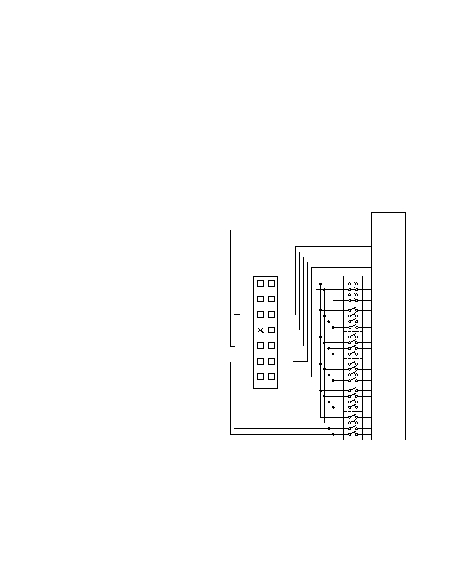
DESIGNING AN EZ-ICE-COMPATIBLE SYSTEM
The ADSP-21mod970 has on-chip emulation support and an
ICE-Port, a special set of pins that interface to the EZ-ICE.
These features allow in-circuit emulation without replacing the
target system processor by using only a 14-pin connection from
the target system to the EZ-ICE. Target systems must have a
14-pin connector to accept the EZ-ICE's in-circuit probe, a
14-pin plug.
The EZ-ICE can emulate only one modem processor at a time.
You must include hardware to select which processor in the
ADSP-21mod970 you want to emulate. Figure 10 is a functional
representation of the modem processor selection hardware. You
can use one ICE-Port connector with two ADSP-21mod970
processors without using additional buffers.
Issuing the "chip reset" command during emulation causes the
modem processor to perform a full chip reset, including a reset
of its memory mode. Therefore, it is vital that the mode pins are
set correctly PRIOR to issuing a chip reset command from the
emulator user interface. As the mode pins share functionality
with PF0:3 on the ADSP-21mod970, it may be necessary to
reset the target hardware separately to insure the proper mode
selection state on emulator chip reset. See the ADSP-2100 Fam-
ily EZ-Tools data sheet for complete information on ICE products.
The ICE-Port interface consists of the following ADSP-21mod970
pins:
EBR
EMS
ELIN
EBG
EINT
ELOUT
ERESET
ECLK
EE
These ADSP-21mod970 pins must be connected only to the
EZ-ICE connector in the target system. These pins have no
function except during emulation, and do not require pull-up or
pull-down resistors. The traces for these signals between the
ADSP-21mod970 and the connector must be kept as short as
possible, no longer that 3 inches.
1
3
5
7
9
11
13
2
4
6
8
10
12
14
BG
BR
EINT
ELIN
ECLK
EMS
ERESET
GND
EBG
EBR
KEY
ELOUT
EE
RESET
ELOUT
EBR
EBG
EINT
ELIN
ECLK
EMS
ERESET
BG0
BR0
RESET0
EE0
ADSP-21
mod970
BG1
BR1
RESET1
EE1
BG2
BR2
RESET2
EE2
BG3
BR3
RESET3
EE3
BG4
BR4
RESET4
EE4
BG5
BR5
RESET5
EE5
ICE-PORT
CONNECTOR
Figure 10. Selecting a Modem Processor in the
ADSP-21mod970
The following pins are also used by the EZ-ICE:
BR
BG
RESET
GND
The EZ-ICE uses the EE (emulator enable) signal to take con-
trol of the ADSP-21mod970 in the target system. This causes
the processor to use its ERESET, EBR and EBG pins instead of
the RESET, BR and BG pins. The BG output is three-stated.
These signals do not need to be jumper-isolated in a system.
ADSP-21mod970
13
REV. 0
The EZ-ICE connects to target system via a ribbon cable and a
14-pin female plug. The female plug is plugged onto the 14-pin
connector (a pin strip header) on the target board.
Target Board Connector for EZ-ICE Probe
The EZ-ICE connector (a standard pin strip header) is shown in
Figure 11. This connector must be added to the target board
design if the EZ-ICE is to be used. Be sure to allow enough
room in the system to fit the EZ-ICE probe onto the 14-pin
connector.
BG
BR
EINT
ELIN
ECLK
EMS
ERESET
GND
EBG
EBR
KEY (NO PIN)
ELOUT
EE
RESET
Figure 11. Target Board Connector for EZ-ICE
The 14-pin, 2-row pin strip header is keyed at the Pin 7 loca-
tion--you must remove Pin 7 from the header. The pins must
be 0.025 inch square and at least 0.20 inch in length. Pin spac-
ing should be 0.1
×
0.1 inches. The pin strip header must have
at least 0.15 inch clearance on all sides to accept the EZ-ICE
probe plug.
Pin strip headers are available from vendors such as 3M,
McKenzie, and Samtec.
Target Memory Interface
For your target system to be compatible with the EZ-ICE emu-
lator, it must comply with the memory interface guidelines listed
below.
PM, DM, BM, IOM, and CM
Design the Program Memory (PM), Data Memory (DM), Byte
Memory (BM), I/O Memory (IOM) and Composite Memory
(CM) external interfaces to comply with worst case device tim-
ing requirements and switching characteristics as specified in
this data sheet. The performance of the EZ-ICE may approach
published worst case specification for some memory access
timing requirements and switching characteristics.
Note: If your target does not meet the worst case chip specifica-
tion for memory access parameters, you may not be able to
emulate your circuitry at the desired CLKIN frequency. De-
pending on the severity of the specification violation, you may
have trouble manufacturing your system as processor compo-
nents statistically vary in switching characteristic and timing
requirements within published limits.
Restriction: All memory strobe signals on the ADSP-21mod970
(RD, WR, PMS, DMS, BMS, CMS, and IOMS) used in your
target system must have 10 k
pull-up resistors connected when
the EZ-ICE is being used. The pull-up resistors are necessary
because there are no internal pull-ups to guarantee their state
during prolonged three-state conditions resulting from typical
EZ-ICE debugging sessions. These resistors may be removed at
your option when the EZ-ICE is not being used.
Target System Interface Signals
When the EZ-ICE board is installed, the performance on some
system signals changes. Design your system to be compatible
with the following system interface signal changes introduced by
the EZ-ICE board:
·
EZ-ICE emulation introduces an 8 ns propagation delay
between your target circuitry and the processor on the
RESET signal.
·
EZ-ICE emulation introduces an 8 ns propagation delay
between your target circuitry and the processor on the BR
signal.
·
EZ-ICE emulation ignores RESET and BR when single-
stepping.
·
EZ-ICE emulation ignores RESET and BR when in Emula-
tor Space (processor halted).
·
EZ-ICE emulation ignores the state of target BR in certain
modes. As a result, the target system may take control of the
processor's external memory bus only if bus grant (BG) is
asserted by the EZ-ICE board's processor.

14
ADSP-21mod970SPECIFICATIONS
REV. 0
RECOMMENDED OPERATING CONDITIONS
K Grade
Parameter
Min
Max
Unit
V
DD
3.15
3.45
V
T
AMB
0
+70
°
C
ELECTRICAL CHARACTERISTICS
K/B Grades
Parameter
Test Conditions
Min
Typ
Max
Unit
V
IH
Hi-Level Input Voltage
1, 2
@ V
DD
= max
2.0
V
V
IH
Hi-Level CLKIN Voltage
@ V
DD
= max
2.2
V
V
IL
Lo-Level Input Voltage
1, 3
@ V
DD
= min
0.8
V
V
OH
Hi-Level Output Voltage
1, 4, 5
@ V
DD
= min
I
OH
= 0.5 mA
2.4
V
@ V
DD
= min
I
OH
= 100
µ
A
6
V
DD
0.3
V
V
OL
Lo-Level Output Voltage
1, 4, 5
@ V
DD
= min
I
OL
= 2 mA
0.4
V
I
IH
Hi-Level Input Current
3
@ V
DD
= max
V
IN
= V
DD
max
10
µ
A
I
IL
Lo-Level Input Current
3
@ V
DD
= max
V
IN
= 0 V
10
µ
A
I
OZH
Three-State Leakage Current
7
@ V
DD
= max
V
IN
= V
DD
max
8
10
µ
A
I
OZL
Three-State Leakage Current
7
@ V
DD
= max
V
IN
= 0 V
8
10
µ
A
I
DD
Supply Current (Idle)
9
@ V
DD
= 3.3
µ
A
t
CK
= 19 ns
10
62
mA
t
CK
= 25 ns
10
53
mA
t
CK
= 30 ns
10
47
mA
I
DD
Supply Current (Dynamic)
11
@ V
DD
= 3.3
T
AMB
= +25
°
C
t
CK
= 19 ns
10
387
mA
t
CK
= 25 ns
10
299
mA
t
CK
= 30 ns
10
253
mA
C
I
Input Pin Capacitance
6
@ V
IN
= 2.5 V,
f
IN
= 1.0 MHz,
40
pF
C
O
Output Pin Capacitance
6, 7, 12
T
AMB
= +25
°
C
@ V
IN
= 2.5 V,
f
IN
= 1.0 MHz,
T
AMB
= +25
°
C
40
pF
NOTES
1
Bidirectional pins: D0-D23, RFS0, RFS1, SCLK0, SCLK1, TFS0, TFS1, A1A13, PF0PF7.
2
Input only pins: RESET, BR, DR0, DR1, PWD.
3
Input only pins: CLKIN, RESET, BR, DR0, DR1, PWD.
4
Output pins: BG, PMS, DMS, BMS, IOMS, CMS, RD, WR, PWDACK, A0, DT0, DT1, CLKOUT, FL20, BGH.
5
Although specified for TTL outputs, all ADSP-21mod970 outputs are CMOS-compatible and will drive to V
DD
and GND, assuming no dc loads.
6
Guaranteed but not tested.
7
Three-statable pins: A0A13, D0D23, PMS, DMS, BMS, IOMS, CMS, RD, WR, DT0, DT1, SCLK0, SCLK1, TFS0, TFS1, RFS0, RFS1.
8
0 V on BR.
9
Idle refers to ADSP-21mod970 state of operation during execution of IDLE instruction. Deasserted pins are driven to either V
DD
or GND.
10
V
IN
= 0 V and 3 V. For typical figures for supply currents, refer to Power Dissipation section.
11
I
DD
measurement taken with all instructions executing from internal memory. 50% of the instructions are multifunction (types 1, 4, 5, 12, 13, 14), 30% are type 2
and type 6, and 20% are idle instructions.
12
Output pin capacitance is the capacitive load for any three-stated output pin.
Specifications subject to change without notice.
ADSP-21mod970
15
REV. 0
ABSOLUTE MAXIMUM RATINGS*
Supply Voltage . . . . . . . . . . . . . . . . . . . . . . . 0.3 V to +4.6 V
Input Voltage . . . . . . . . . . . . . . . . . . . . 0.5 V to V
DD
+ 0.5 V
Output Voltage Swing . . . . . . . . . . . . . 0.5 V to V
DD
+ 0.5 V
Storage Temperature Range . . . . . . . . . . . . 65
°
C to +150
°
C
*Stresses above those listed under Absolute Maximum Ratings may cause perma-
nent damage to the device. These are stress ratings only; functional operation of
the device at these or any other conditions above those indicated in the operational
sections of this specification is not implied. Exposure to absolute maximum rating
conditions for extended periods may affect device reliability.
TIMING PARAMETERS
GENERAL NOTES
Use the exact timing information given. Do not attempt to
derive parameters from the addition or subtraction of others.
While addition or subtraction would yield meaningful results for
an individual device, the values given in this data sheet reflect
statistical variations and worst cases. Consequently, you cannot
meaningfully add up parameters to derive longer times.
TIMING NOTES
Switching characteristics specify how the processor changes its
signals. You have no control over this timing--circuitry external
to the processor must be designed for compatibility with these
signal characteristics. Switching characteristics tell you what the
processor will do in a given circumstance. You can also use
switching characteristics to ensure that any timing requirement
of a device connected to the processor (such as memory) is
satisfied.
Timing requirements apply to signals that are controlled by
circuitry external to the processor, such as the data input for a
read operation. Timing requirements guarantee that the proces-
sor operates correctly with other devices.
MEMORY TIMING SPECIFICATIONS
Table VI shows common memory device specifications and the
corresponding ADSP-21mod970 timing parameter.
Table VI. Memory Devices and Timing Parameters
ADSP-
Memory
21mod970
Timing
Device
Timing
Parameter
Specification
Parameter
Definition
Address Setup to
t
ASW
A0A13, xMS Setup
Write Start
before WR Low
Address Setup to
t
AW
A0A13, xMS Setup
Write End
before WR Deasserted
Address Hold Time
t
WRA
A0A13, xMS Hold
before WR Low
Data Setup Time
t
DW
Data Setup before WR
High
Data Hold Time
t
DH
Data Hold after WR High
OE to Data Valid
t
RDD
RD Low to Data Valid
Address Access Time
t
AA
A0A13, xMS to Data
Valid
Note: xMS = PMS, DMS, BMS, CMS, IOMS.
FREQUENCY DEPENDENCY FOR TIMING
SPECIFICATIONS
t
CK
is defined as 0.5 t
CKI
. The ADSP-21mod970 uses an input
clock with a frequency equal to half the instruction rate: a
26.32 MHz input clock (which is equivalent to 38.0 ns) yields a
19 ns processor cycle (equivalent to 52 MHz). t
CK
values within
the range of 0.5 t
CKI
period should be substituted for all relevant
timing parameters to obtain the specification value.
Example: t
CKH
= 0.5 t
CK
7 ns = 0.5 (19 ns) 7 ns = 2.5 ns
ENVIRONMENTAL CONDITIONS
Ambient Temperature Rating:
T
AMB
=
T
J
(PD
×
JA
)
T
J
=
Junction Temperature in
°
C
PD
=
Power Dissipation in W
JA
=
Thermal Resistance (Junction-to-Ambient)
Package
JA
PBGA
26.9
°
C/W
ESD SENSITIVITY
ESD (electrostatic discharge) sensitive device. Electrostatic charges as high as 4000 V readily
accumulate on the human body and test equipment and can discharge without detection. Although
the ADSP-21mod970 features proprietary ESD protection circuitry, permanent damage may occur
on devices subjected to high energy electrostatic discharges. Therefore, proper ESD precautions are
recommended to avoid performance degradation or loss of functionality.
WARNING!
ESD SENSITIVE DEVICE
ADSP-21mod970
16
REV. 0
POWER DISSIPATION
To determine total power dissipation in a specific application,
the following equation should be applied for each output:
C
×
V
DD
2
×
f
C = load capacitance, f = output switching frequency.
204.6
79.2
223.2
204.6
186
169.2
FREQUENCY MHz
1200
33.3
52
800
600
POWER, INTERNAL
3.6V
3.3V
3.0V
1537.2
1277.1
1029
1008
834.9
678
POWER mW
1000
FREQUENCY MHz
33.33
52
V
DD
= 3.6V
V
DD
= 3.3V
V
DD
= 3.0V
155.1
141
POWER mW
FREQUENCY MHz
33.33
POWER, IDLE
n MODES
52
IDLE
155.1
POWER mW
70
210
90
110
130
150
170
190
1400
1600
POWER, IDLE
150
100
200
250
82.4076
83.0709
86.3709
IDLE (16)
IDLE (128)
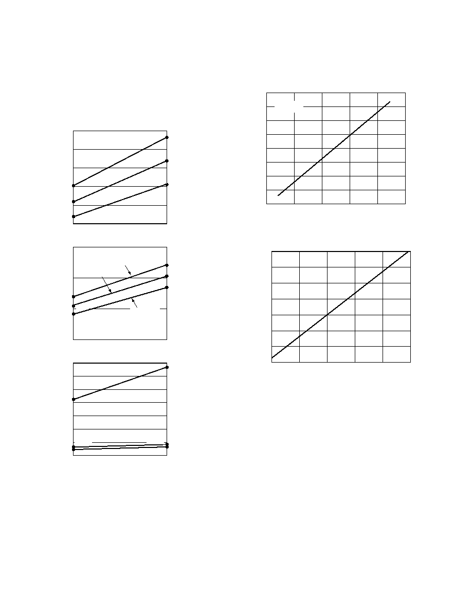
Figure 12. Power vs. Frequency
CAPACITIVE LOADING
Figures 13 and 14 show the capacitive loading characteristics of
the ADSP-21mod970.
C
L
pF
4
0
250
RISE TIME (0.4V 2.4V) ns
18
6
8
10
12
14
16
20
50
100
150
200
T = +85 C
V
DD
= +3.0V
Figure 13. Typical Output Rise Time vs. Load Capaci-
tance, C
L
(at Maximum Ambient Operating Temperature)
C
L
pF
4
0
200
VALID OUTPUT DELAY
OR HOLD ns
10
2
2
4
6
8
40
80
120
160
NOMINAL
Figure 14. Typical Output Valid Delay or Hold vs. Load
Capacitance, C
L
(at Maximum Ambient Operating
Temperature)
ADSP-21mod970
17
REV. 0
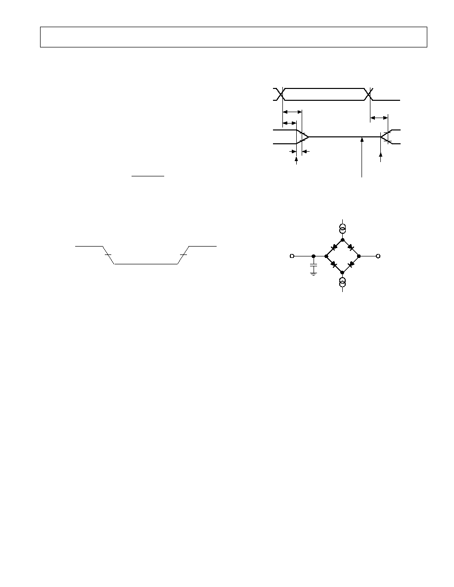
TEST CONDITIONS
Output Disable Time
Output pins are considered to be disabled when they have
stopped driving and started a transition from the measured
output high or low voltage to a high impedance state. The out-
put disable time (t
DIS
) is the difference between t
MEASURED
and
t
DECAY,
as shown in Figure 15. The time is the interval from
when a reference signal reaches a high or low voltage level to
when the output voltages have changed by 0.5 V from the mea-
sured output high or low voltage.
The decay time, t
DECAY
, is dependent on the capacitive load,
C
L
, and the current load, i
L
, on the output pin. It can be ap-
proximated by the following equation:
t
C
V
i
DECAY
L
L
=
×
0 5
.
from which
t
DIS
= t
MEASURED
t
DECAY
is calculated. If multiple pins (such as the data bus) are dis-
abled, the measurement value is that of the last pin to stop
driving.
1.5V
INPUT
OR
OUTPUT
1.5V
Figure 15. Voltage Reference Levels for AC Measure-
ments (Except Output Enable/Disable)
Output Enable Time
Output pins are considered to be enabled when they have made
a transition from a high impedance state to when they start
driving. The output enable time (t
ENA
) is the interval from when
a reference signal reaches a high or low voltage level to when the
output has reached a specified high or low trip point, as shown
in Figure 16. If multiple pins (such as the data bus) are enabled,
the measurement value is that of the first pin to start driving.
2.0V
1.0V
t
ENA
REFERENCE
SIGNAL
OUTPUT
t
DECAY
V
OH
(MEASURED)
OUTPUT STOPS
DRIVING
OUTPUT STARTS
DRIVING
t
DIS
t
MEASURED
V
OL
(MEASURED)
V
OH
(MEASURED) 0.5V
V
OL
(MEASURED) +0.5V
HIGH IMPEDANCE STATE. TEST CONDITIONS CAUSE
THIS VOLTAGE LEVEL TO BE APPROXIMATELY 1.5V.
V
OH
(MEASURED)
V
OL
(MEASURED)
Figure 16. Output Enable/Disable
TO
OUTPUT
PIN
50pF
+1.5V
I
OH
I
OL
Figure 17. Equivalent Device Loading for AC Measure-
ments (Including All Fixtures)
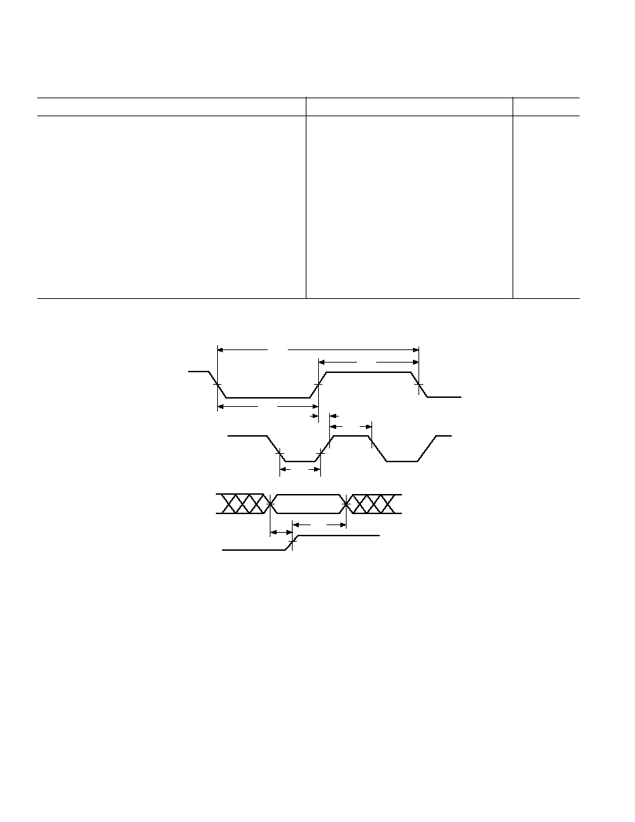
ADSP-21mod970
18
REV. 0
TIMING PARAMETERS
Parameter
Min
Max
Unit
Clock Signals and Reset
Timing Requirements:
t
CKI
CLKIN Period
38
100
ns
t
CKIL
CLKIN Width Low
15
ns
t
CKIH
CLKIN Width High
15
ns
Switching Characteristics:
t
CKL
CLKOUT Width Low
0.5 t
CK
7
ns
t
CKH
CLKOUT Width High
0.5 t
CK
7
ns
t
CKOH
CLKIN High to CLKOUT High
0
20
ns
Control Signals
Timing Requirements:
t
RSP
RESET Width Low
5 t
CK
1
ns
t
MS
Mode Setup before RESET High
2
ns
t
MH
Mode Setup after RESET High
5
ns
NOTE
1
Applies after power-up sequence is complete. Internal phase lock loop requires no more than 2000 CLKIN cycles assuming stable CLKIN (not including crystal
oscillator start-up time).
t
CKOH
t
CKI
t
CKIH
t
CKIL
t
CKH
t
CKL
t
MH
t
MS
CLKIN
CLKOUT
PF(3:0)
*
RESET
*
PF3 IS MODE D, PF2 IS MODE C, PF1 IS MODE B, PF0 IS MODE A
Figure 18. Clock Signals
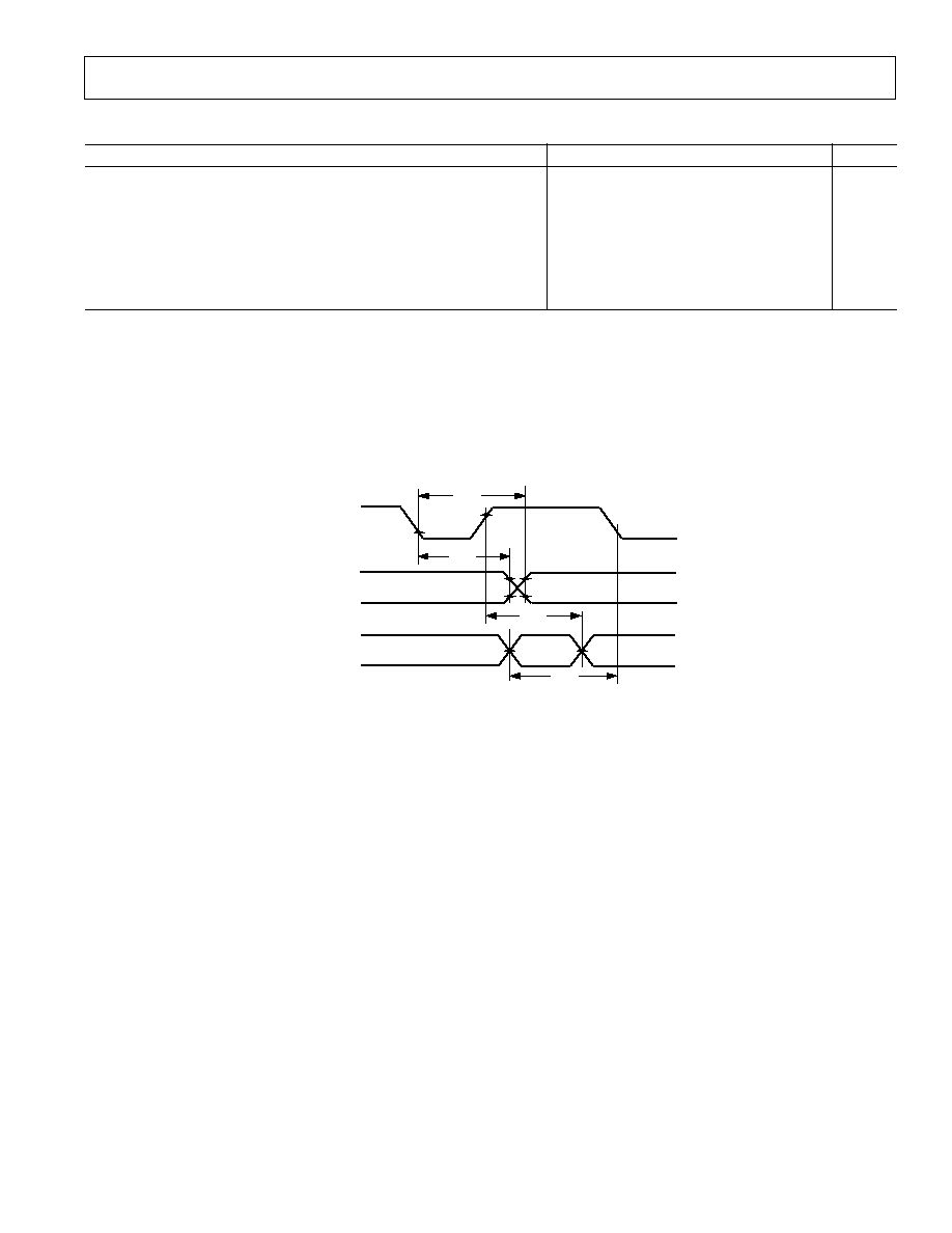
ADSP-21mod970
19
REV. 0
Parameter
Min
Max
Unit
Interrupts and Flags
Timing Requirements:
t
IFS
IRQx, FI, or PFx Setup before CLKOUT Low
1, 2, 3, 4
0.25 t
CK
+ 15
ns
t
IFH
IRQx, FI, or PFx Hold after CLKOUT High
1, 2, 3, 4
0.25 t
CK
ns
Switching Characteristics:
t
FOH
Flag Output Hold after CLKOUT Low
5
0.25 t
CK
7
ns
t
FOD
Flag Output Delay from CLKOUT Low
5
0.5 t
CK
+ 6
ns
NOTES
1
If IRQx and FI inputs meet t
IFS
and t
IFH
setup/hold requirements, they will be recognized during the current clock cycle; otherwise the signals will be recognized on the
following cycle. (Refer to Interrupt Controller Operation in the Program Control chapter of the ADSP-2100 Family User's Manual, Third Edition, for further information
on interrupt servicing.)
2
Edge-sensitive interrupts require pulsewidths greater than 10 ns; level-sensitive interrupts must be held low until serviced.
3
IRQx = IRQ0, IRQ1, IRQ2, IRQL0, IRQL1, IRQE.
4
PFx = PF0, PF1, PF2, PF3, PF4, PF5, PF6, PF7.
5
Flag outputs = PFx, FL0, FL1, FL2, Flag_out.
t
FOD
t
FOH
t
IFH
t
IFS
CLKOUT
FLAG
OUTPUTS
IRQx
FI
PFx
Figure 19. Interrupts and Flags
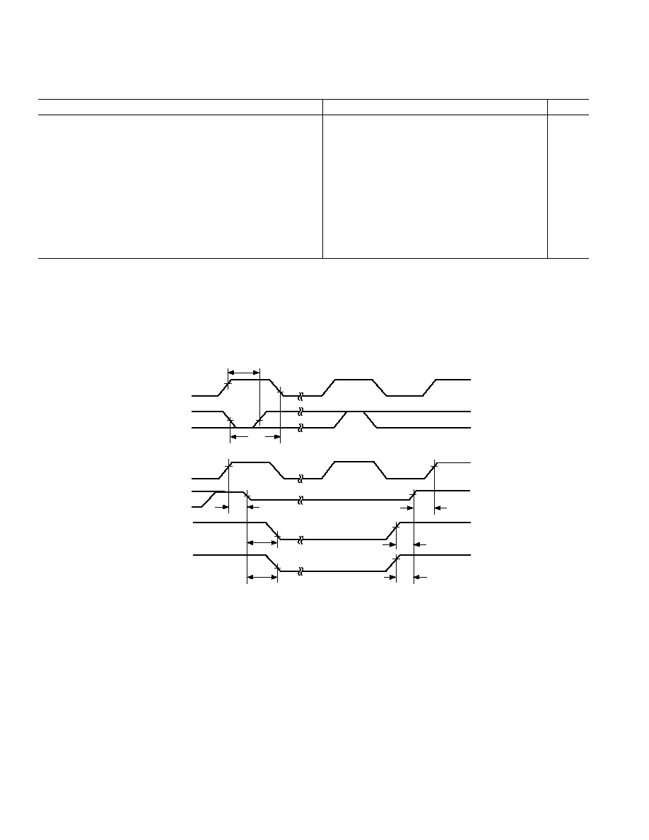
ADSP-21mod970
20
REV. 0
TIMING PARAMETERS
Parameter
Min
Max
Unit
Bus RequestBus Grant
Timing Requirements:
t
BH
BR Hold after CLKOUT High
1
0.25 t
CK
+ 2
ns
t
BS
BR Setup before CLKOUT Low
1
0.25 t
CK
+ 17
ns
Switching Characteristics:
t
SD
CLKOUT High to xMS, RD, WR Disable
0.25 t
CK
+ 10
ns
t
SDB
xMS, RD, WR Disable to BG Low
0
ns
t
SE
BG High to xMS, RD, WR Enable
0
ns
t
SEC
xMS, RD, WR Enable to CLKOUT High
0.25 t
CK
4
ns
t
SDBH
xMS, RD, WR Disable to BGH Low
2
0
ns
t
SEH
BGH High to xMS, RD, WR Enable
2
0
ns
NOTES
xMS = PMS, DMS, CMS, IOMS, BMS.
1
BR is an asynchronous signal. If BR meets the setup/hold requirements, it will be recognized during the current clock cycle; otherwise the signal will be recognized
on the following cycle. Refer to the ADSP-2100 Family User's Manual, Third Edition, for BR/BG cycle relationships.
2
BGH is asserted when the bus is granted and the processor requires control of the bus to continue.
CLKOUT
t
SD
t
SDB
t
SE
t
SEC
t
SDBH
t
SEH
t
BS
BR
t
BH
CLKOUT
PMS
,
DMS
BMS
,
RD
WR
BG
BGH
Figure 20. Bus RequestBus Grant
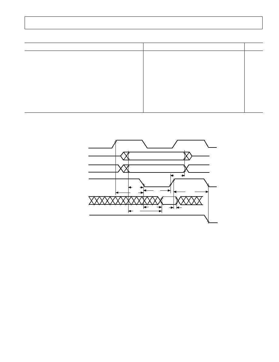
ADSP-21mod970
21
REV. 0
Parameter
Min
Max
Unit
Memory Read
Timing Requirements:
t
RDD
RD Low to Data Valid
0.5 t
CK
9 + w
ns
t
AA
A0A13, xMS to Data Valid
0.75 t
CK
12.5 + w
ns
t
RDH
Data Hold from RD High
0
ns
Switching Characteristics:
t
RP
RD Pulsewidth
0.5 t
CK
5 + w
ns
t
CRD
CLKOUT High to RD Low
0.25 t
CK
5
0.25 t
CK
+ 7
ns
t
ASR
A0A13, xMS Setup before RD Low
0.25 t
CK
6
ns
t
RDA
A0A13, xMS Hold after RD Deasserted
0.25 t
CK
3
ns
t
RWR
RD High to RD or WR Low
0.5 t
CK
5
ns
w = wait states
×
t
CK
.
xMS = PMS, DMS, CMS, IOMS, BMS.
CLKOUT
A0A13
D
t
RDA
t
RWR
t
RP
t
ASR
t
CRD
t
RDD
t
AA
t
RDH
DMS
,
PMS
,
BMS
,
IOMS
,
CMS
RD
WR
Figure 21. Memory Read
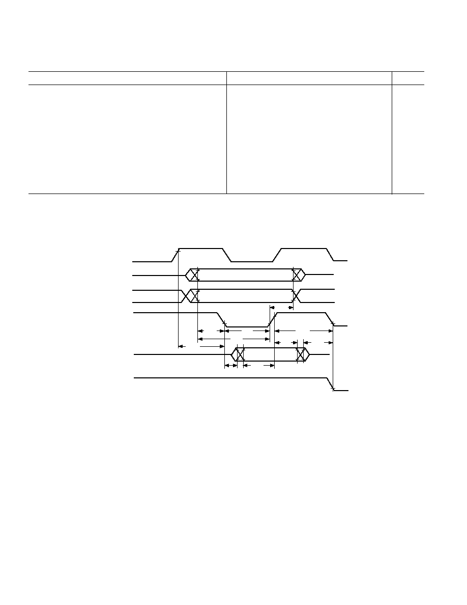
ADSP-21mod970
22
REV. 0
TIMING PARAMETERS
Parameter
Min
Max
Unit
Memory Write
Switching Characteristics:
t
DW
Data Setup before WR High
0.5 t
CK
7 + w
ns
t
DH
Data Hold after WR High
0.25 t
CK
2
ns
t
WP
WR Pulsewidth
0.5 t
CK
5 + w
ns
t
WDE
WR Low to Data Enabled
0
ns
t
ASW
A0A13, xMS Setup before WR Low
0.25 t
CK
6
ns
t
DDR
Data Disable before WR or RD Low
0.25 t
CK
7
ns
t
CWR
CLKOUT High to WR Low
0.25 t
CK
5
0.25 t
CK
+ 7
ns
t
AW
A0A13, xMS, Setup before WR Deasserted
0.75 t
CK
9 + w
ns
t
WRA
A0A13, xMS Hold after WR Deasserted
0.25 t
CK
3
ns
t
WWR
WR High to RD or WR Low
0.5 t
CK
5
ns
w = wait states
×
t
CK
.
xMS = PMS, DMS, CMS, IOMS, BMS.
CLKOUT
A0A13
D
t
WP
t
AW
t
CWR
t
DH
t
WDE
t
DW
t
ASW
t
WWR
t
WRA
t
DDR
DMS
,
PMS
,
BMS
,
CMS
,
IOMS
RD
WR
Figure 22. Memory Write
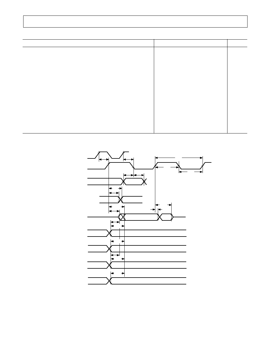
ADSP-21mod970
23
REV. 0
Parameter
Min
Max
Unit
Serial Ports
Timing Requirements:
t
SCK
SCLK Period
38
ns
t
SCS
DR/TFS/RFS Setup before SCLK Low
4
ns
t
SCH
DR/TFS/RFS Hold after SCLK Low
7
ns
t
SCP
SCLK
IN
Width
15
ns
Switching Characteristics:
t
CC
CLKOUT High to SCLK
OUT
0.25 t
CK
0.25 t
CK
+ 10
ns
t
SCDE
SCLK High to DT Enable
0
ns
t
SCDV
SCLK High to DT Valid
15
ns
t
RH
TFS/RFS
OUT
Hold after SCLK High
0
ns
t
RD
TFS/RFS
OUT
Delay from SCLK High
15
ns
t
SCDH
DT Hold after SCLK High
0
ns
t
TDE
TFS (Alt) to DT Enable
0
ns
t
TDV
TFS (Alt) to DT Valid
14
ns
t
SCDD
SCLK High to DT Disable
15
ns
t
RDV
RFS
(Multichannel, Frame Delay Zero) to DT Valid
15
ns
CLKOUT
SCLK
TFS
OUT
RFS
OUT
DT
ALTERNATE
FRAME MODE
t
CC
t
CC
t
SCS
t
SCH
t
RH
t
SCDE
t
SCDH
t
SCDD
t
TDE
t
RDV
MULTICHANNEL MODE,
FRAME DELAY 0
(MFD = 0)
DR
TFS
IN
RFS
IN
RFS
OUT
TFS
OUT
t
TDV
t
SCDV
t
RD
t
SCP
t
SCK
t
SCP
TFS
IN
RFS
IN
ALTERNATE
FRAME MODE
t
RDV
MULTICHANNEL MODE,
FRAME DELAY 0
(MFD = 0)
t
TDV
t
TDE
Figure 23. Serial Ports
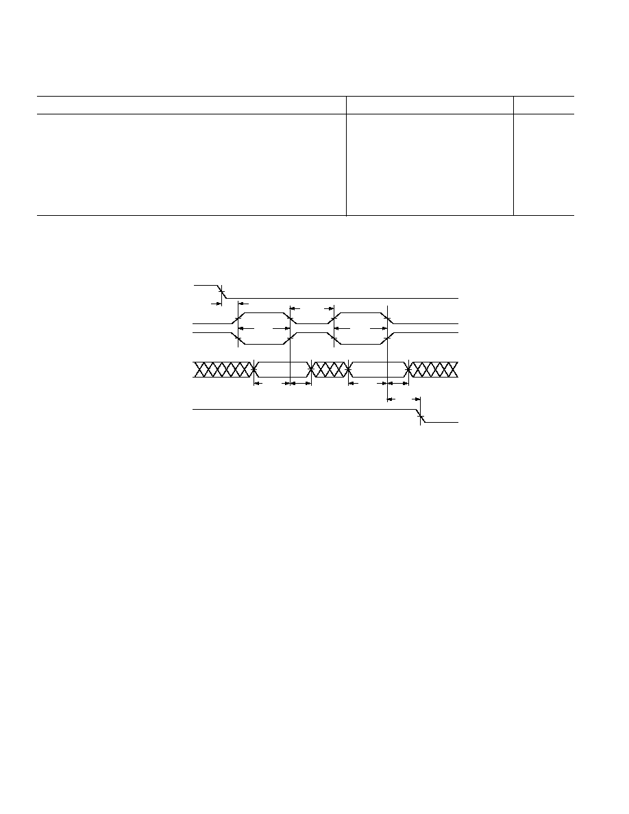
ADSP-21mod970
24
REV. 0
TIMING PARAMETERS
Parameter
Min
Max
Unit
IDMA Address Latch
Timing Requirements:
t
IALP
Duration of Address Latch
1, 2
10
ns
t
IASU
IAD150 Address Setup before Address Latch End
2
5
ns
t
IAH
IAD150 Address Hold after Address Latch End
2
2
ns
t
IKA
IACK Low before Start of Address Latch
2, 3
0
ns
t
IALS
Start of Write or Read after Address Latch End
1, 2
3
ns
t
IALD
Address Latch Start after Address Latch End
1, 2
2
ns
NOTES
1
Start of Address Latch = IS Low and IAL High.
2
End of Address Latch = IS High or IAL Low.
3
Start of Write or Read = IS Low and IWR Low or IRD Low.
IACK
IAL
IS
IAD150
RD
OR
WR
t
IKA
t
IALP
t
IALD
t
IASU
t
IAH
t
IASU
t
IALS
t
IAH
t
IALP
Figure 24. IDMA Address Latch
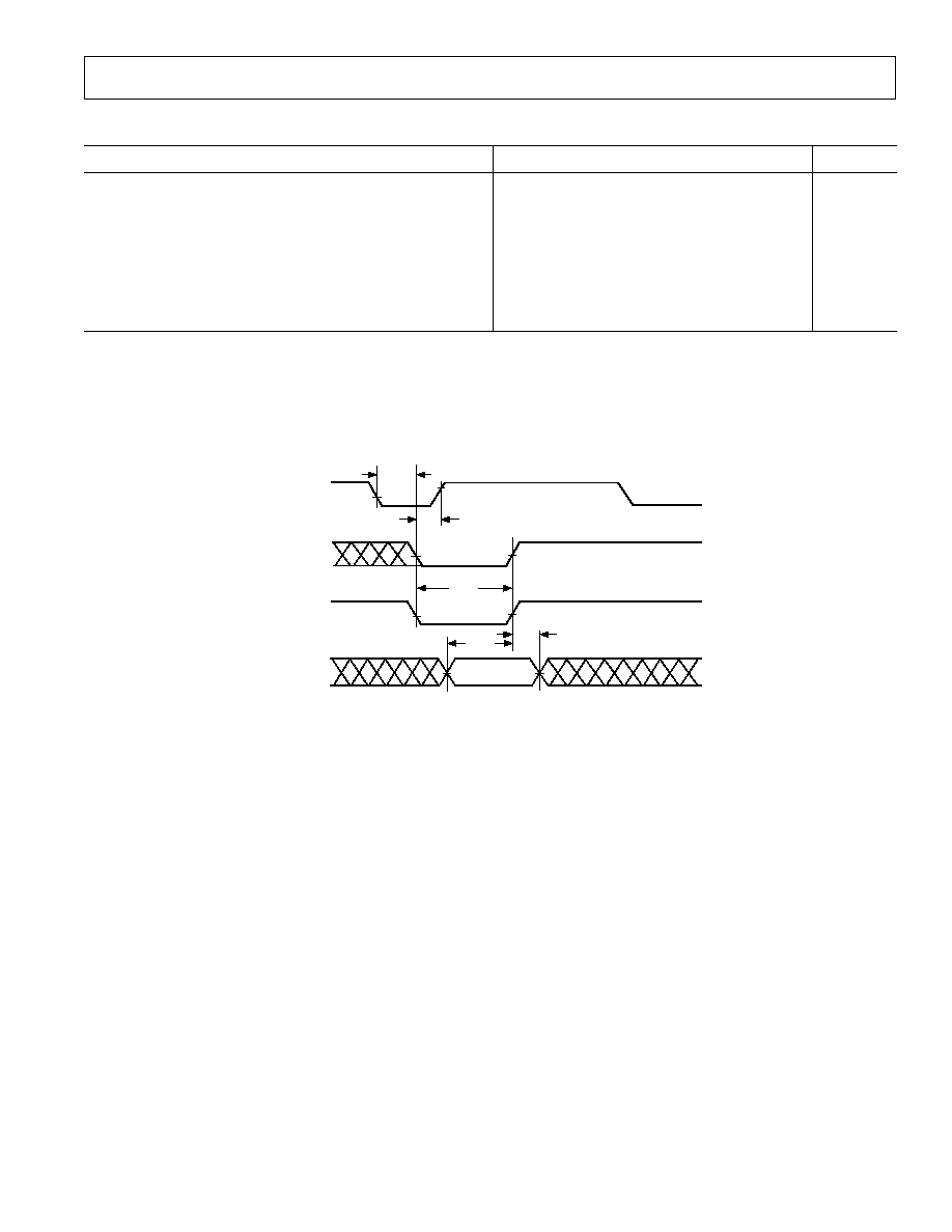
ADSP-21mod970
25
REV. 0
Parameter
Min
Max
Unit
IDMA Write, Short Write Cycle
Timing Requirements:
t
IKW
IACK Low before Start of Write
1
0
ns
t
IWP
Duration of Write
1, 2
15
ns
t
IDSU
IAD150 Data Setup before End of Write
2, 3, 4
5
ns
t
IDH
IAD150 Data Hold after End of Write
2, 3, 4
2
ns
Switching Characteristic:
t
IKHW
Start of Write to IACK High
4
15
ns
NOTES
1
Start of Write = IS Low and IWR Low.
2
End of Write = IS High or IWR High.
3
If Write Pulse ends before IACK Low, use specifications t
IDSU
, t
IDH
.
4
If Write Pulse ends after IACK Low, use specifications t
IKSU
, t
IKH
.
IAD150
DATA
t
IKHW
t
IKW
t
IDSU
IACK
t
IWP
t
IDH
IS
IWR
Figure 25. IDMA Write, Short Write Cycle
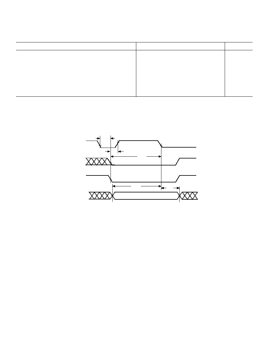
ADSP-21mod970
26
REV. 0
TIMING PARAMETERS
Parameter
Min
Max
Unit
IDMA Write, Long Write Cycle
Timing Requirements:
t
IKW
IACK Low before Start of Write
1
0
ns
t
IKSU
IAD150 Data Setup before IACK Low
2, 3, 4
0.5 t
CK
+ 10
ns
t
IKH
IAD150 Data Hold after IACK Low
2, 3, 4
2
ns
Switching Characteristics:
t
IKLW
Start of Write to IACK Low
4
1.5 t
CK
ns
t
IKHW
Start of Write to IACK High
4
15
ns
NOTES
1
Start of Write = IS Low and IWR Low.
2
If Write Pulse ends before IACK Low, use specifications t
IDSU
, t
IDH
.
3
If Write Pulse ends after IACK Low, use specifications t
IKSU
, t
IKH
.
4
This is the earliest time for IACK Low from Start of Write. For IDMA Write cycle relationships, please refer to the ADSP-2100 Family User's Manual, Third Edition.
IAD150
DATA
t
IKHW
t
IKW
IACK
IS
IWR
t
IKLW
t
IKH
t
IKSU
Figure 26. IDMA Write, Long Write Cycle
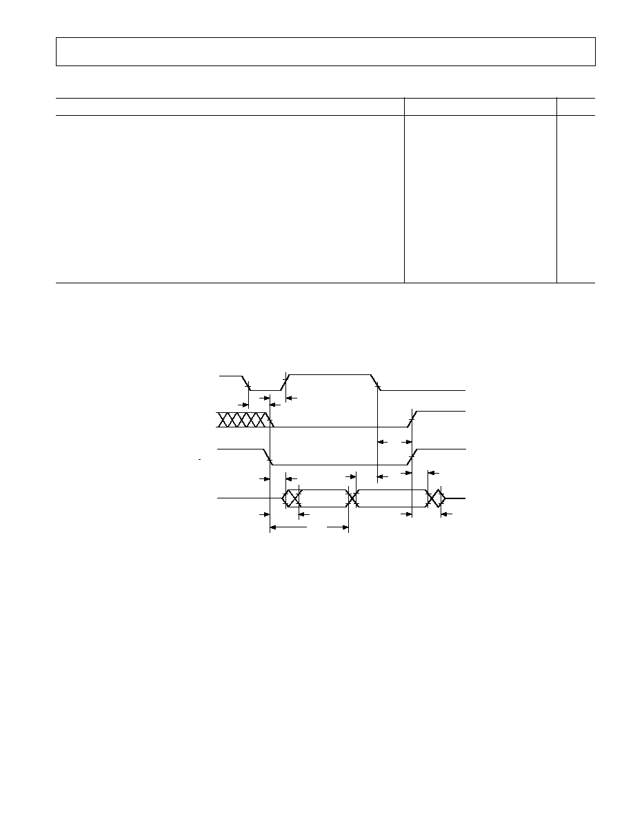
ADSP-21mod970
27
REV. 0
Parameter
Min
Max
Unit
IDMA Read, Long Read Cycle
Timing Requirements:
t
IKR
IACK Low before Start of Read
1
0
ns
t
IRK
End of Read after IACK Low
2
2
ns
Switching Characteristics:
t
IKHR
IACK High after Start of Read
1
4
15
ns
t
IKDS
IAD150 Data Setup before IACK Low
0.5 t
CK
7
ns
t
IKDH
IAD150 Data Hold after End of Read
2
0
ns
t
IKDD
IAD150 Data Disabled after End of Read
2
10
ns
t
IRDE
IAD150 Previous Data Enabled after Start of Read
0
ns
t
IRDV
IAD150 Previous Data Valid after Start of Read
10
ns
t
IRDH1
IAD150 Previous Data Hold after Start of Read (DM/PM1)
3
2 t
CK
5
ns
t
IRDH2
IAD150 Previous Data Hold after Start of Read (PM2)
4
t
CK
5
ns
NOTES
1
Start of Read = IS Low and IRD Low.
2
End of Read = IS High or IRD High.
3
DM read or first half of PM read.
4
Second half of PM read.
t
IRK
t
IKR
PREVIOUS
DATA
READ
DATA
t
IKHR
t
IKDS
t
IRDV
t
IRDH
t
IKDD
t
IRDE
t
IKDH
IAD150
IACK
IS
IRD
Figure 27. IDMA Read, Long Read Cycle
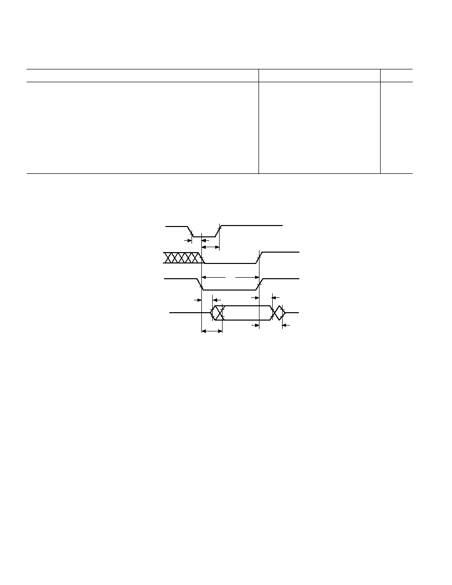
ADSP-21mod970
28
REV. 0
TIMING PARAMETERS
Parameter
Min
Max
Unit
IDMA Read, Short Read Cycle
Timing Requirements:
t
IKR
IACK Low before Start of Read
1
0
ns
t
IRP
Duration of Read
15
ns
Switching Characteristics:
t
IKHR
IACK High after Start of Read
1
4
15
ns
t
IKDH
IAD150 Data Hold after End of Read
2
0
ns
t
IKDD
IAD150 Data Disabled after End of Read
2
10
ns
t
IRDE
IAD150 Previous Data Enabled after Start of Read
0
ns
t
IRDV
IAD150 Previous Data Valid after Start of Read
10
ns
NOTES
1
Start of Read = IS Low and IRD Low.
2
End of Read = IS High or IRD High.
t
IRP
t
IKR
PREVIOUS
DATA
t
IKHR
t
IRDV
t
IKDD
t
IRDE
t
IKDH
IAD150
IACK
IS
IRD
Figure 28. IDMA Read, Short Read Cycle

ADSP-21mod970
29
REV. 0
304-Ball PBGA Package Pinout
The ADSP-21mod970 package pinout is shown in the table below.
Ball
Signal
Ball
Signal
Ball
Signal
Ball
Signal
Number
Name
Number
Name
Number
Name
Number
Name
A1
GND
B23
IAD1
D22
IAD4
K4
CMS_1
A2
PF0_1
C1
IAD5_1
D23
IAD3
K20
PF5_3
A3
PF2_1
C2
IAD0_1
E1
IAD8_1
K21
EBG
A4
FL1_1
C3
GND
E2
IAD7_1
K22
EBR
A5
D23_1
C4
BGH_1
E3
IAD2_1
K23
EINT
A6
D21_1
C5
PF3_1
E4
IAD1_1
L1
D17
A7
D13_1
C6
FL2_1
E20
CLKIN
L2
D18
A8
D16_1
C7
D12_1
E21
GND
L3
PF5_1
A9
GND
C8
D17_1
E22
GND
L4
PF7_1
A10
PF0_2
C9
GND
E23
GND
L20
V
DD
A11
PF1_2
C10
IAD13_1
F1
IAD12_1
L21
ERESET
A12
FL0_2
C11
IAD15_1
F2
IAD9_1
L22
ELIN
A13
FL1_2
C12
PF2_2
F3
IAD10_1
L23
ELOUT
A14
V
DD
C13
V
DD
F4
IWR_1
M1
D15
A15
V
DD
C14
V
DD
F20
GND
M2
D16
A16
PF0_3
C15
V
DD
F21
GND
M3
PF6_1
A17
PF1_3
C16
IS_2
F22
GND
M4
BGH_4
A18
FL0_3
C17
CLKOUT_2
F23
GND
M20
V
DD
A19
FL1_3
C18
PF4_2
G1
CLKIN_1
M21
V
DD
A20
D21
C19
DT1_2
G2
IAD11_1
M22
V
DD
A21
D22
C20
EE_2
G3
D8_1
M23
V
DD
A22
D23
C21
GND
G4
IRD_1
N1
D13
A23
GND
C22
IAD2
G20
IAL
N2
D12
B1
IAD3_1
C23
IAD0
G21
IRD
N3
D14
B2
GND
D1
IAD6_1
G22
IWR
N4
PF1_4
B3
PF1_1
D2
IAD4_1
G23
GND
N20
V
DD
B4
FL0_1
D3
A0_1
H1
RD_1
N21
PF6_3
B5
D22_1
D4
GND
H2
WR_1
N22
ECLK
B6
D20_1
D5
D10_1
H3
IAL_1
N23
EMS
B7
D19_1
D6
D11_1
H4
IS_1
P1
GND
B8
D15_1
D7
D9_1
H20
CLKOUT_3
P2
GND
B9
GND
D8
D18_1
H21
RFS0A
P3
GND
B10
D14_1
D9
GND
H22
DR0A
P4
TFS0_1
B11
BGH_2
D10
IAD14_1
H23
IS_3
P20
DT1_3
B12
PF3_2
D11
BR_1
J1
DMS_1
P21
PF2_6
B13
FL2_2
D12
BG_1
J2
BMS_1
P22
RESET_3
B14
V
DD
D13
IACK_1
J3
PMS_1
P23
EE_3
B15
V
DD
D14
V
DD
J4
CLKOUT_1
R1
IAD6
B16
BGH_3
D15
V
DD
J20
SCLK0A
R2
IAD7
B17
PF2_3
D16
BG_2
J21
PF4_3
R3
IAD5
B18
PF3_3
D17
BR_2
J22
BG_3
R4
PF0_4
B19
FL2_3
D18
PF5_2
J23
BR_3
R20
PF0_6
B20
D20
D19
RESET_2
K1
D19
R21
PF1_6
B21
DT0A
D20
GND
K2
PF4_1
R22
FL2_6
B22
GND
D21
GND
K3
IOMS_1
R23
FL1_6
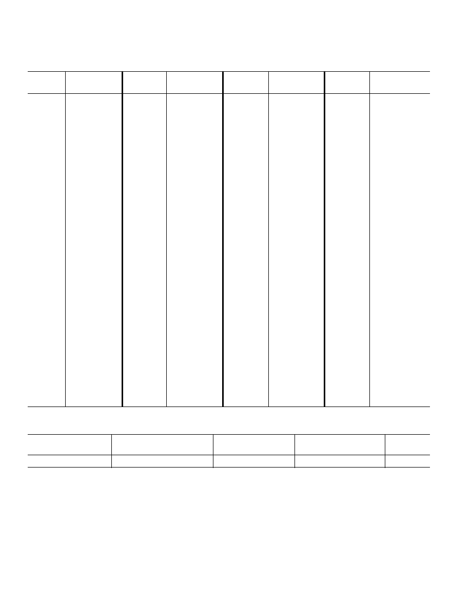
ADSP-21mod970
30
REV. 0
304-Ball PBGA Package Pinout (continued)
Ball
Signal
Ball
Signal
Ball
Signal
Ball
Signal
Number
Name
Number
Name
Number
Name
Number
Name
T1
D10
W23
GND
AA8
PF4_5
AB16
PF2_5
T2
D9
Y1
V
DD
AA9
GND
AB17
CLKOUT_6
T3
D11
Y2
V
DD
AA10
PF6_5
AB18
RFS0B
T4
EE_1
Y3
V
DD
AA11
V
DD
AB19
GND
T20
BGH_6
Y4
GND
AA12
DT1_5
AB20
SCLK0B
T21
TFS0_3
Y5
FL0_4
AA13
BGH_5
AB21
RESET_6
T22
PF3_6
Y6
V
DD
AA14
PF7_2
AB22
GND
T23
FL0_6
Y7
FL2_4
AA15
PF1_5
AB23
BG_6
U1
IAD9
Y8
CLKOUT_5
AA16
FL1_5
AC1
GND
U2
IAD11
Y9
GND
AA17
TFS1
AC2
BR_4
U3
IAD8
Y10
IS_5
AA18
DR1
AC3
PF7_4
U4
PF2_4
Y11
V
DD
AA19
GND
AC4
GND
U20
GND
Y12
TFS0_2
AA20
DT1_6
AC5
TFS0_4
U21
GND
Y13
PF6_2
AA21
GND
AC6
V
DD
U22
GND
Y14
PF0_5
AA22
BG_5
AC7
V
DD
U23
GND
Y15
FL0_5
AA23
IAD14
AC8
GND
V1
IAD10
Y16
FL2_5
AB1
PF5_4
AC9
GND
V2
IAD12
Y17
RFS1
AB2
GND
AC10
TFS0_5
V3
DT1_1
Y18
SCLK1
AB3
PF6_4
AC11
V
DD
V4
PF3_4
Y19
GND
AB4
GND
AC12
EE_5
V20
GND
Y20
GND
AB5
DT1_4
AC13
PF5_6
V21
GND
Y21
BR_5
AB6
V
DD
AC14
GND
V22
GND
Y22
IAD13
AB7
RESET_4
AC15
PF6_6
V23
GND
Y23
IACK
AB8
PF5_5
AC16
PF7_6
W1
D8
AA1
PF4_4
AB9
GND
AC17
DT0B
W2
CLKOUT_4
AA2
BG_4
AB10
PF7_5
AC18
TFS0_6
W3
RESET_1
AA3
GND
AB11
V
DD
AC19
GND
W4
IS_4
AA4
GND
AB12
RESET_5
AC20
DR0B
W20
IS_6
AA5
FL1_4
AB13
PF4_6
AC21
EE_6
W21
PF7_3
AA6
V
DD
AB14
GND
AC22
BR_6
W22
IAD15
AA7
EE_4
AB15
PF3_5
AC23
GND
ORDERING GUIDE
Part
Ambient
Package
Package
Number
Temperature Range
Processor Clock
Description
Option
ADSP-21mod970-000
0
°
C to +70
°
C
26.0 MHz
304-Ball PBGA
B-304
RELATED DOCUMENTS
ADSP-21mod970-110 Multiport Internet Gateway Processor solution.
ADSP-21mod970
31
REV. 0
GND
IAD3
1
IAD8
1
IAD12
1
CLKIN
1
RD
1
DMS
1
D19
D17
D15
D13
GND
IAD6
D10
IAD9
IAD10
D8
V
DD
PF4
4
PF5
4
GND
IAD5
1
IAD6
1
1
PF0
1
GND
IAD7
1
IAD9
1
IAD11
1
WR
1
BMS
1
PF4
1
D18
D16
D12
GND
IAD7
D9
IAD11
IAD12
CLK
OUT
4
V
DD
BG
4
GND
BR
4
IAD0
1
IAD4
1
2
PF2
1
PF1
1
IAD2
1
IAD10
1
D8
1
IAL
1
PMS
1
IOMS
1
PF5
1
PF6
1
D14
GND
IAD5
D11
IAD8
DT1
1
RESET
1
V
DD
GND
PF6
4
PF7
4
GND
A0
1
3
FL1
1
FL0
1
IAD1
1
IWR
1
IRD
1
IS
1
CLK
OUT
1
CMS
1
PF7
1
BGH
4
PF1
4
TFS0
1
PF0
4
EE
1
PF2
4
PF3
4
IS
4
GND
GND
GND
GND
BGH
1
GND
4
D23
1
D22
1
FL0
4
FL1
4
DT1
4
TFS0
4
PF3
1
D10
1
5
D21
1
D20
1
V
DD
V
DD
V
DD
V
DD
FL2
1
D11
1
6
D13
1
D19
1
FL2
4
EE
4
RESET
4
V
DD
D12
1
D9
1
7
D16
1
D15
1
CLK
OUT
5
PF4
5
PF5
5
GND
D17
1
D18
1
8
GND
GND
TFS0
2
DT1
5
RESET
5
EE
5
GND
GND
9
PF0
2
D14
1
GND
GND
GND
GND
IAD13
1
1AD14
1
10
PF1
2
BGH
2
IS
5
PF6
5
PF7
5
TFS0
5
IAD15
1
BR
1
11
FL0
2
PF3
2
V
DD
V
DD
V
DD
V
DD
PF2
2
BG
1
12
FL1
2
FL2
2
PF6
2
BGH
5
PF4
6
PF5
6
V
DD
IACK
1
13
V
DD
V
DD
PF0
5
PF7
2
GND
GND
V
DD
V
DD
14
V
DD
V
DD
FL0
5
PF1
5
PF3
5
PF6
6
V
DD
V
DD
15
PF0
3
BGH
3
RFS1
TFS1
CLK
OUT
6
DT0B
IS
2
BG
2
16
PF1
3
PF2
3
SCLK1
DR1
RFS0B
TFS0
6
CLK
OUT
2
BR
2
17
FL0
3
PF3
3
GND
GND
GND
GND
PF4
2
PF5
2
18
FL1
3
FL2
3
DT1
2
RESET
2
19
D21
D20
CLKIN
GND
IAL
CLK
OUT
3
SCLK0A
PF5
3
V
DD
V
DD
V
DD
DT1
3
PF0
6
BGH
6
GND
GND
IS
6
GND
DT1
6
SCLK0B
DR0B
EE_2
GND
20
D22
DT0A
GND
GND
IRD
RFS0A
PF4
3
EBG
ERESET
V
DD
PF6
3
PF2
6
PF1
6
TFS0
3
GND
GND
PF7
3
BR
5
GND
RESET
6
EE
6
GND
GND
21
D23
GND
GND
GND
IWR
DR0A
BG
3
EBR
ELIN
V
DD
ECLK
RESET
3
FL2
6
PF3
6
GND
GND
IAD15
IAD13
BG
5
GND
BR
6
IAD2
IAD4
22
GND
IAD1
GND
GND
GND
IS
3
BR
3
EINT
ELOUT
V
DD
EMS
EE
3
FL1
6
FL0
6
GND
GND
GND
IACK
IAD14
BG
GND
IAD0
IAD3
23
PIN
A
B
C
D
E
F
G
H
J
K
L
M
N
P
R
T
U
V
W
Y
AA
AB
AC
1
2
3
4
5
6
7
8
9
10
11
12
13
14
15
16
17
18
19
20
21
22
23
A
B
C
D
E
F
G
H
J
K
L
M
N
P
R
T
U
V
W
Y
AA
AB
AC
FL2
5
FL1
5
PF2
5
PF7
6
ADSP-21mod970
(TOP VIEW)
NOTE: THE NUMBER AFTER THE UNDERSCORE IN SIGNAL NAMES CORRESPONDS TO THE MODEM CHANNEL
NUMBER IN THE FUNCTIONAL BLOCK DIAGRAM ON PAGE 1. ANY SIGNAL NAME WITHOUT AN UNDERSCORE
CORRESPONDS TO SIGNALS BEING SHARED AMONG MODEM CHANNELS NUMBER 26.
ADSP-21mod970 Pinout
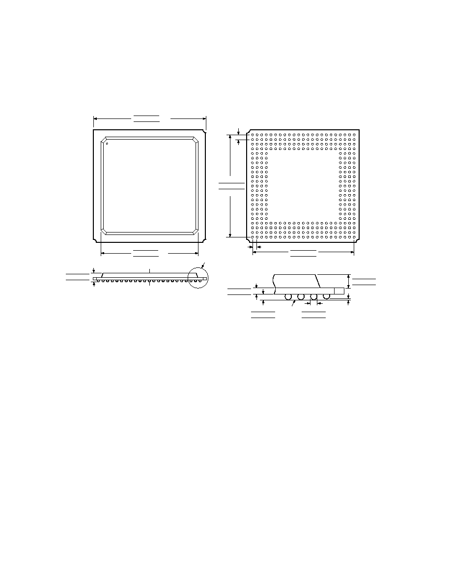
ADSP-21mod970
32
OUTLINE DIMENSIONS
Dimensions shown in inches and (mm).
C34942.57/99
PRINTED IN U.S.A.
REV. 0
304-Ball Metric Plastic Ball Grid Array
(B-304)
0.048 (1.22)
0.046 (1.17)
0.044 (1.12)
SEATING
PLANE
0.008 (0.20)
MAX
DETAIL A
0.035 (0.90)
0.030 (0.75)
0.024 (0.60)
BALL DIAMETER
0.024 (0.62)
0.022 (0.56)
0.020 (0.50)
0.028 (0.70)
0.024 (0.60)
0.020 (0.50)
DETAIL A
0.100 (2.54)
0.092 (2.33)
0.083 (2.12)
1.224 (31.10)
1.220 (31.00) SQ
1.217 (30.90)
1.051 (26.70)
1.037 (26.35) SQ
1.024 (26.00)
TOP VIEW
0.050 (1.27)
BSC
1.104 (28.04)
1.100 (27.94)
1.096 (27.84)
0.050 (1.27)
BSC
BOTTOM VIEW
A
B
C
D
E
F
G
H
J
K
L
M
N
P
R
T
U
V
W
Y
AA
AB
AC
23 22 21 20 19 18 17 16 15 14 13 12 11 10 9 8 7 6 5 4 3 2 1
1.104 (28.04)
1.100 (27.94)
1.096 (27.84)
NOTE
1. THE ACTUAL POSITION OF THE BALL GRID IS WITHIN 0.012 (0.30)
OF THE IDEAL POSITION RELATIVE TO THE PACKAGE EDGES.
2. THE ACTUAL POSITION OF EACH BALL IS WITHIN 0.004 (0.10) OF ITS
IDEAL POSITION RELATIVE TO THE BALL GRID.
3. CENTER FIGURES ARE TYPICAL UNLESS OTHERWISE NOTED.