Äîêóìåíòàöèÿ è îïèñàíèÿ www.docs.chipfind.ru
REV. B
Information furnished by Analog Devices is believed to be accurate and
reliable. However, no responsibility is assumed by Analog Devices for its
use, nor for any infringements of patents or other rights of third parties that
may result from its use. No license is granted by implication or otherwise
under any patent or patent rights of Analog Devices. Trademarks and
registered trademarks are the property of their respective owners.
One Technology Way, P.O. Box 9106, Norwood, MA 02062-9106, U.S.A.
Tel: 781/329-4700
www.analog.com
Fax: 781/326-8703
© 2004 Analog Devices, Inc. All rights reserved.
ADP3806
High Frequency Switch Mode
Li-Ion Battery Charger
FEATURES
Li-Ion Battery Charger
Three Battery Voltage Options
Selectable 12.525 V/16.700 V
Selectable 12.600 V/16.800 V
Adjustable
High End-of-Charge Voltage Accuracy
0.4% @ 25 C
0.6% @ 5 C to 55 C
0.7% @ 0 C to 85 C
Programmable Charge Current with Rail-to-Rail
Sensing
System Current Sense with Reverse Input Protection
Soft-Start Charge Current
Undervoltage Lockout
Bootstrapped Synchronous Drive for External NMOS
Programmable Oscillator Frequency
Oscillator SYNC Pin
Low Current Flag
Trickle Charge
APPLICATIONS
Portable Computers
Fast Chargers
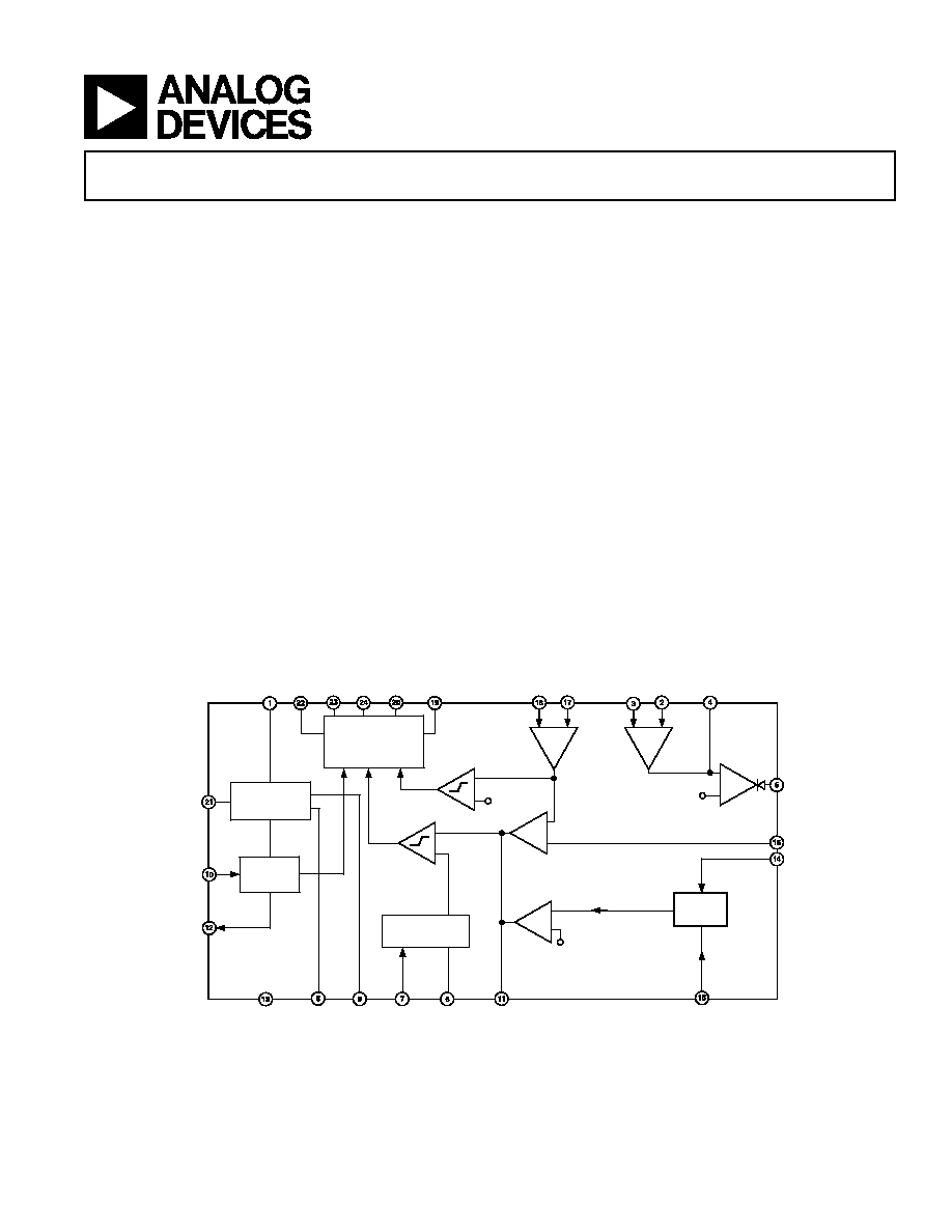
FUNCTIONAL BLOCK DIAGRAM
gm2
+
SELECT
12.6/16.8
BOOTSTRAPPED
SYNCHRONOUS
DRIVER
CS+
OSCILLATOR
VREF + VREG
UVLO
BIAS
CS
COMP
REF
AGND
BAT
SD
CT
SW
REG
PGND
VCC
BST
DRVH
DRVL
SYS+ SYS
ISYS
ISET
LOGIC
CONTROL
LC
SYNC
LIMIT
VREF
2.5V
VREF
ADP3806
BSTREG
BATSEL
SD
IN DRVLSD
V
TH
DRVLSD
gm1
+
+
+
+
+
AMP1
+
AMP2
+
+
GENERAL DESCRIPTION
The ADP3806 is a complete Li-Ion battery-charging IC. The
device combines high output voltage accuracy with constant
current control to simplify the implementation of constant-
current, constant-voltage (CCCV) chargers. The ADP3806 is
available in three options: The ADP3806-12.6 guarantees the
final battery voltage selected is 12.6 V or 16.8 V
± 0.6%, the
ADP3806-12.5 guarantees 12.525 V/16.7 V
± 0.6%, and the
ADP3806 is adjustable using two external resistors to set the
battery voltage. The current sense amplifier has rail-to-rail inputs
to accurately operate under low dropout and short-circuit condi-
tions. The charge current is programmable with a dc voltage on
ISET. A second differential amplifier senses the system current
across an external sense resistor and outputs a linear voltage
on the ISYS pin. The bootstrapped synchronous driver allows
the use of two NMOS transistors for lower system cost.

REV. B
2
ADP3806SPECIFICATIONS
1
(@ 0 C
£ T
A
£ 100 C, VCC = 16 V, unless otherwise noted.)
Parameter
Conditions
Symbol
Min
Typ
Max
Unit
BATTERY SENSE INPUT
ADP3806-12.6 V and 16.8 V
ADP3806-12.525 V and 16.7 V
T
A
= 25
C, 13 V £ VCC £ 20 V
V
BAT
0.4
+0.4
%
5
C £ T
A
£ 55C
V
BAT
0.6
+0.6
%
0
C £ T
A
£ 85C
V
BAT
0.7
+0.7
%
Input Resistance
Part in Operation
R
BAT
250
350
k
W
Input Current
Part in Shutdown
I
BAT(SD)
0.2
1.0
mA
BATTERY SENSE INPUT
ADP3806
V
BAT
= 2.5 V
T
A
= 25
C, 13 V £ VCC £ 20 V
V
BAT
0.5
+0.5
%
0
C £ T
A
£ 85C
V
BAT
0.7
+0.7
%
Input Current Operating
BATSEL = Open, Part in Operation
0.2
1.0
mA
Input Current Shutdown
BATSEL = 100 k
W to GND, Part in Shutdown
0.2
1.0
mA
OSCILLATOR
Maximum Frequency
2
f
CT
1000
kHz
Frequency Variation
3
CT = 180 pF
f
CT
210
250
290
kHz
CT Charge Current
I
CT
125
150
175
mA
0% Duty Cycle Threshold
@ COMP Pin
1.0
V
Maximum Duty Cycle Threshold
@ COMP Pin
2.5
V
SYNC Input High
SYNC
H
2.2
V
SYNC Input Low
SYNC
L
0.8
V
SYNC Input Current
I
SYNC
0.2
1.0
mA
GATE DRIVE
On Resistance
I
L
= 10 mA
R
ON
6
10
W
Rise, Fall Time
C
L
= 1 nF, DRVL and DRVH
t
r
, t
f
35
ns
Overlap Protection Delay
DRVL Falling to DRVH Rising,
t
OP
50
ns
DRVH Falling to DRVL Rising
SW Bias Current
Part in Shutdown, V
SW
= 12.6 V
0.2
1.0
mA
BST Cap Refresh Threshold
V
BST
V
SW
3.7
V
CURRENT SENSE AMPLIFIER
Input Common-Mode Range
V
CS+
and V
CS
V
CS(CM)
0.0
VCC + 0.3
V
Input Differential Mode Range
V
CS
4
V
CS(DM)
0.0
160
mV
Input Offset Voltage
5
0 V
£ V
CS(CM)
£ VCC
V
CS(VOS)
1.0
mV
Gain
5
25
V/V
Input Bias Current
0 V
£ V
CS(CM)
£ VCC, Part in Operation
V
CS(IB)
50
100
mA
Input Offset Current
0 V
£ V
CS(CM)
£ VCC
V
CS(IOS)
1.0
2.0
mA
Input Bias Current
Part in Shutdown
0.2
1.0
mA
DRVL Shutdown Threshold
Measured between V
CS+
and V
CS
V
CS(SD
)
48
mV
SYSTEM CURRENT SENSE
6
Input Common-Mode Range
SYS+ and SYS, I
L
= 0 mA, V
ISYS
= 3 V
V
SYS(CM)
4.0
VCC + 0.3
V
Input Differential Range
(V
SYS+
) (V
SYS
)
V
SYS(DM)
0
100
mV
Input Offset Voltage
0.5
mV
Input Bias Current, SYS+
V
SYS(DM)
= 0 V, V
SYS(CM)
= 16 V
I
B(SYS+)
200
300
mA
Input Bias Current, SYS
V
SYS(DM)
= 0 V, V
SYS(CM)
= 16 V
I
B(SYS)
70
125
mA
Voltage Gain
10 V
£ V
SYS(CM)
£ VCC + 0.3 V, I
L
= 100
mA
48.5
50
51.5
V/V
Output Range
I
L
= 1 mA
7
, V
SYS(CM)
> 6 V
V
ISYS
0
5.0
V
Limit Output Threshold
V
LIMIT
£ 0.2 V, 50 kW Pull-up to 5 V
V
TH(LIMIT)
2.3
2.5
2.7
V
Limit Output Voltage
V
ISYS
> 2.65 V, I
SINK
= 700
mA
V
O(LIMIT)
0.1
0.2
V
ISET INPUT
Charge Current Programming
Function
0.0 V < V
ISET
£ 4.0 V
V
ISET/VCS
25
V/V
Programming Function Accuracy
V
ISET
= 4.0 V, 1 V
£ V
CS(CM)
£ 16 V
5
±1.0
+5
%
V
ISET
= 0.50 V, 1 V
£ V
CS(CM)
£ 10 V
30
±10
+30
%
5
C £ T
A
£ 55C, V
ISET
= 206 mV,
46.7
+33
%
V
CS(CM)
= 5 V and 10 V
ISET Bias Current
0.0 V
£ V
ISET
£ 4.0 V
I
B
0.2
1.0
mA

REV. B
ADP3806
3
Parameter
Conditions
Symbol
Min
Typ
Max
Unit
BATSEL INPUT
V
BAT
= 12.6 V
2.0
V
V
BAT
= 16.8 V
0.8
V
BATSEL Input Current
0.2
5.0
mA
BOOST REGULATOR OUTPUT
Output Voltage
C
L
= 0.1
mF
V
BSTREG
6.8
7.0
7.2
V
Output Current
8
I
BSTREG
3.0
5.0
mA
ANALOG REGULATOR OUTPUT
Output Voltage
C
L
= 10 nF
V
REG
5.8
6.0
6.2
V
Output Current
8
I
REG
3.0
5.0
mA
PRECISION REFERENCE OUTPUT
Output Voltage
V
REF
2.47
2.5
2.53
V
Output Current
8
I
REF
0.5
1.1
mA
SHUTDOWN (
SD)
ON
SD
H
2.0
V
OFF
SD
L
0.8
V
SD Input Current
0.2
1.0
mA
POWER SUPPLY
ON Supply Current
No External Loads, UVLO
£ VCC £ 20 V
I
SYON
6.0
8.0
mA
OFF Supply Current
No External Loads, VCC
£ 20 V
I
SYOFF
1.0
5.0
mA
UVLO Threshold Voltage
Turn On
V
UVLO
5.65
6.0
6.25
V
UVLO Hysteresis
Turn Off
0.1
0.3
0.5
V
LC OUTPUT
Output Voltage Low
High Current Mode
9
, I
SINK
= 100
mA
0.1
0.4
V
Output Voltage High
Low Current Mode
10
External
V
OUTPUT REVERSE LEAKAGE
PROTECTION
Leakage Current
VCC = Floating, V
BAT
= 12.6 V
I
DISCH
1
5
mA
OVERCURRENT COMPARATOR
Overcurrent Threshold
V
CS(OC)
180
mV
Response Time
V
CS
> 180 mV to COMP < 1 V
t
OC
2
ms
OVERVOLTAGE COMPARATOR
Overvoltage Threshold
V
BAT(OV)
120
%
Response Time
V
BAT
> 120% to COMP < 1 V
t
OV
2
ms
NOTES
1
All limits at temperature extremes are guaranteed via correlation using standard Statistical Quality Control (SQC) methods.
2
Guaranteed by design, not tested in production.
3
If SYNC function is used, then f
SYNC
must be greater than f
CT
but less than 120% of f
CT
.
4
V
CS
= (V
CS+
) (V
CS
).
5
Accuracy guaranteed by ISET input, programming function accuracy specification.
6
System current sense is active during shutdown.
7
Load current is supplied through SYS+ pin.
8
Guaranteed output current from 0 to min specified value to maintain regulation.
9
V
BAT
< 93% of final or V
CS
> 25 mV.
10
V
BAT
93% of final and V
CS
£ 25 mV.
Specifications subject to change without notice.

REV. B
4
ADP3806
CAUTION
ESD (electrostatic discharge) sensitive device. Electrostatic charges as high as 4000 V readily
accumulate on the human body and test equipment and can discharge without detection. Although the
ADP3806 features proprietary ESD protection circuitry, permanent damage may occur on devices
subjected to high energy electrostatic discharges. Therefore, proper ESD precautions are recommended
to avoid performance degradation or loss of functionality.
ABSOLUTE MAXIMUM RATINGS
*
Input Voltage (VCC) . . . . . . . . . . . . . . . . . . . 0.3 V to +25 V
BAT, CS+, CS . . . . . . . . . . . . . . . . . 0.3 V to VCC + 0.3 V
SYS+, SYS . . . . . . . . . . . . . . . . . . . . . . . . . . 25 V to +25 V
BST . . . . . . . . . . . . . . . . . . . . . . . . . . . . . . . . . 0.3 V to +30 V
BST to SW . . . . . . . . . . . . . . . . . . . . . . . . . . . 0.3 V to +8 V
SW to PGND . . . . . . . . . . . . . . . . . . . . . . . . . . 4 V to +25 V
DRVL to PGND . . . . . . . . . . . . . . . . . . . . . . . 0.3 V to +8 V
ISET, BATSEL,
SD, SYNC, CT,
LIMIT, ISYS, LC . . . . . . . . . . . . . . . . . . . 0.3 V to +10 V
COMP . . . . . . . . . . . . . . . . . . . . . . . . . . . . . . . 0.3 V to +3 V
GND to PGND . . . . . . . . . . . . . . . . . . . . . . . 0.3 V to +0.3 V
ORDERING GUIDE
Battery
Package
Package
Quantity
Model
Voltage
Description
Option
per Reel
ADP3806JRU-REEL
Adjustable
TSSOP-24
RU-24
2500
ADP3806JRU-REEL7
Adjustable
TSSOP-24
RU-24
1000
ADP3806JRU-12.5-RL
12.525 V/16.7 V
TSSOP-24
RU-24
2500
ADP3806JRUZ-12.5RL
*
12.525 V/16.7 V
TSSOP-24
RU-24
2500
ADP3806JRU-12.5-R7
12.525 V/16.7 V
TSSOP-24
RU-24
1000
ADP3806JRU-12.6-RL
12.600 V/16.8 V
TSSOP-24
RU-24
2500
ADP3806JRU-12.6-R7
12.600 V/16.8 V
TSSOP-24
RU-24
1000
*Z = Pb-free part.
Operating Ambient Temperature Range . . . . . . 0
C to 100C
JA
. . . . . . . . . . . . . . . . . . . . . . . . . . . . . . . . . . . . . . . 115
C/W
Operating Junction Temperature Range . . . . . . 0
C to 125C
Storage Temperature Range . . . . . . . . . . . . 65
C to +150C
Lead Temperature Range (Soldering 10 sec) . . . . . . . . . 300
C
*Stresses above those listed under Absolute Maximum Ratings may cause perma-
nent damage to the device. This is a stress rating only; functional operation of the
device at these or any other conditions above those listed in the operational
sections of this specification is not implied. Exposure to absolute maximum rating
conditions for extended periods may affect device reliability. Absolute maximum
ratings apply individually only, not in combination. Unless otherwise specified all
other voltages are referenced to GND.
REV. B
ADP3806
5
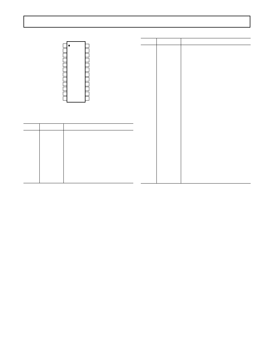
PIN CONFIGURATION
TOP VIEW
(Not to Scale)
24
23
22
21
20
19
18
17
16
15
14
13
1
2
3
4
5
6
7
8
9
10
11
12
ADP3806
LC
COMP
SD
REF
REG
VCC
SYS
SYS+
ISYS
SYNC
CT
LIMIT
AGND
BAT
BATSEL
ISET
CS
SW
DRVH
BST
BSTREG
CS+
PGND
DRVL
PIN FUNCTION DESCRIPTION
Pin No.
Mnemonic Function
1
VCC
Supply Voltage.
2
SYS
Negative System Current Sense Input.
3
SYS+
Positive System Current Sense Input.
4
ISYS
System Current Sense Output.
5
LIMIT
System Current Sense Limit Output.
6
CT
Oscillator Timing Capacitor.
7
SYNC
Oscillator Synchronization Pin.
8
REG
6.0 V Analog Regulator Output.
PIN FUNCTION DESCRIPTION(continued)
Pin No.
Mnemonic Function
9
REF
2.5 V Precision Reference Output.
10
SD
Shutdown Control Input.
11
COMP
External Compensation Node.
12
LC
Low Current Output.
13
AGND
Analog Ground.
14
BAT
Battery Sense Input.
2.5 V for ADP3806.
12.525 V/16.7 V for ADP3806-12.5.
12.6 V/16.8 V for ADP3806-12.6.
15
BATSEL
Battery Voltage Sense Input.
High = 3 Cells, Low = 4 Cells.
16
ISET
Charge Current Program Input.
17
CS
Negative Current Sense Input.
18
CS+
Positive Current Sense Input.
19
PGND
Power Ground.
20
DRVL
Low Drive Output Switches between
REG and PGND.
21
BSTREG
7.0 V Regulator Output for Boost.
22
BST
Floating Bootstrap Supply for DRVH.
23
DRVH
High Drive Output Switches between
SW and BST.
24
SW
Buck Switching Node Reference for
DRVH.
REV. B
6
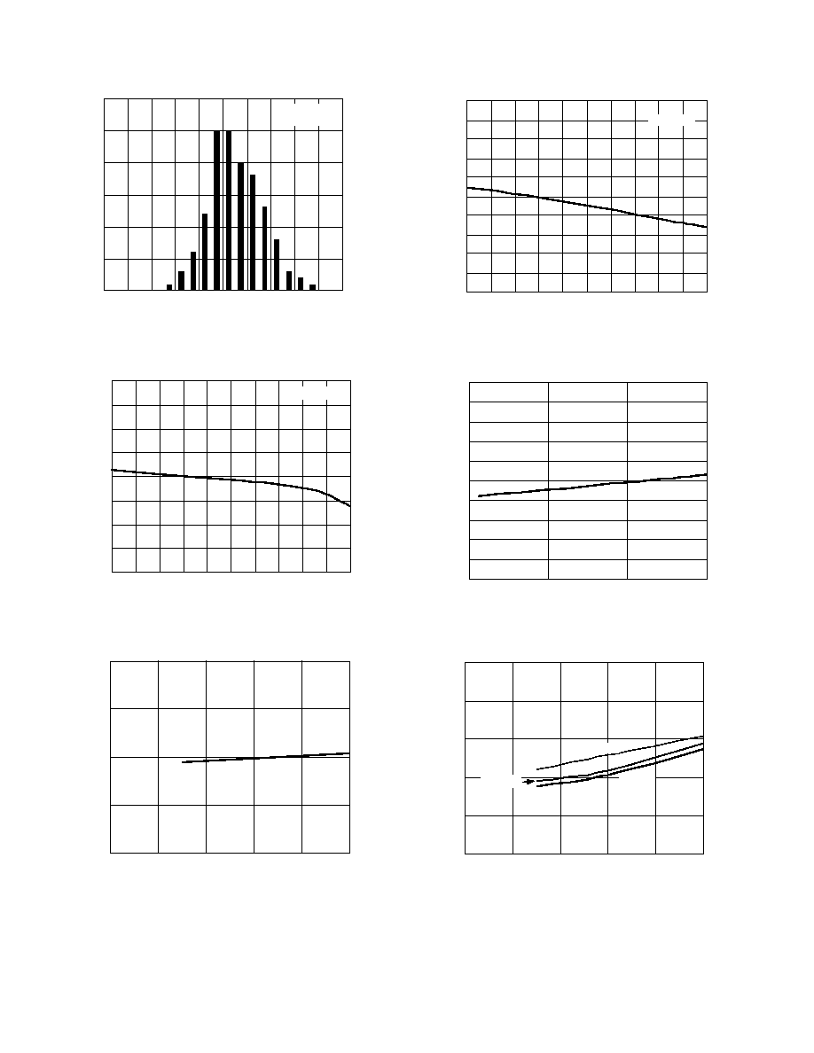
ADP3806Typical Performance Characteristics
0
5
10
15
20
25
30
V
BAT
ACCURACY (%)
VCC = 16V
T
A
= 25 C
NUMBER OF P
A
R
T
S
0.5
0.4
0.3
0.2
0.1
0
0.1
0.2
0.3
0.4
0.5
TPC 1. V
BAT
Accuracy Distribution
0.4
0.3
0.2
0.1
0
0.1
0.2
0.3
0.4
TEMPERATURE ( C)
VCC = 16V
0 20 40 60 80 100
V
BA
T
A
CCURA
CY (%)
TPC 2. V
BAT
Accuracy vs. Temperature
0.10
0.05
0
0.05
0.10
10
12
14
16
18
20
VCC (V)
T
A
= 25 C
V
BA
T
A
CCURA
CY (%)
TPC 3. V
BAT
Accuracy vs. VCC
0.5
0.4
0.3
0.2
0.1
0
0.1
0.2
0.3
0.4
0.5
TEMPERATURE ( C)
VCC = 16V
0 20 40 60 80 100
V
REF
A
CCURA
CY (%)
TPC 4. V
REF
Accuracy vs. Temperature
0.10
0.08
0.06
0.04
0.02
0
0.02
0.04
0.06
0.08
0.10
5
10
15
20
VCC (V)
T
A
= 25 C
V
REF
A
CCURA
CY (%)
TPC 5. V
REF
Accuracy vs. VCC
4.0
4.4
4.8
5.2
5.6
6.0
10
12
14
16
18
20
VCC (V)
NO LOADS
T
A
= 25 C
T
A
= 100 C
T
A
= 0 C
ON SUPPL
Y CURRENT (mA)
TPC 6. ON Supply Current vs. VCC
REV. B
ADP3806
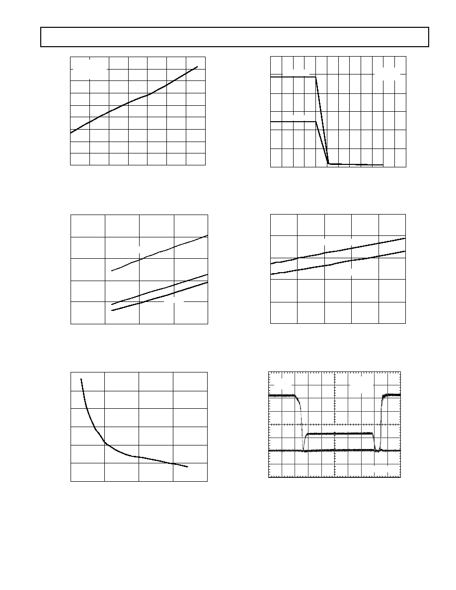
7
0
2
4
6
8
10
12
14
16
18
DRIVER LOAD CAPACITANCE (pF)
VCC = 16V
T
A
= 25 C
f
OSC
= 250kHz
0
SUPPL
Y CURRENT (mA)
500
1000
1500
2000
2500
3000
3500
TPC 7. Supply Current vs. Driver Load Capacitance
0
0.2
0.4
0.6
0.8
1.0
10.0
12.5
15.0
17.5
20.0
VCC (V)
T
A
= 0 C
T
A
= 25 C
T
A
= 100 C
OFF SUPPL
Y CURRENT (
A)
TPC 8. OFF Supply Current vs. VCC
0
100
200
300
400
500
600
0
200
400
600
800
CT (pF)
VCC = 16V
T
A
= 25 C
FREQ
UENCY (kHz)
TPC 9. Oscillator Frequency vs. CT
0
1
2
3
4
5
6
2.0
2.2
2.4
2.6
2.8
3.0
3.2
V
ISYS
(V)
VCC = 16V
T
A
= 25 C
V
LIMIT
(V)
50k TO 5V
50k TO 2.5V
TPC 10. V
LIMIT
vs. V
ISYS
0
2
4
6
8
10
0
20
40
60
80
100
TEMPERATURE ( C)
DRIVER SOURCING
DRIVER SINKING
VCC = 16V
DRIVER ON RESIST
ANCE (
)
TPC 11. Driver On Resistance vs. Temperature
DRVH
5V/DIV
V
CC
= 16V
T
A
= 25 C
FIGURE 1
DRVL 5V/DIV
200ns/DIV
TPC 12. Driver Waveforms
REV. B
8
ADP3806
80
82
84
86
88
90
92
94
96
98
100
0.1
1
10
CHARGE CURRENT (A)
VCC = 19V
V
BAT
= 12.4V
T
A
= 25 C
FIGURE 1
CONVERSION EFFICIENCY (%)
TPC 13. Conversion Efficiency vs. Charge Current
82
84
86
88
90
92
94
96
4
V
BAT
(V)
I
CHARGE
= 2A
I
CHARGE
= 3A
VCC = 19V
T
A
= 25 C
FIGURE 1
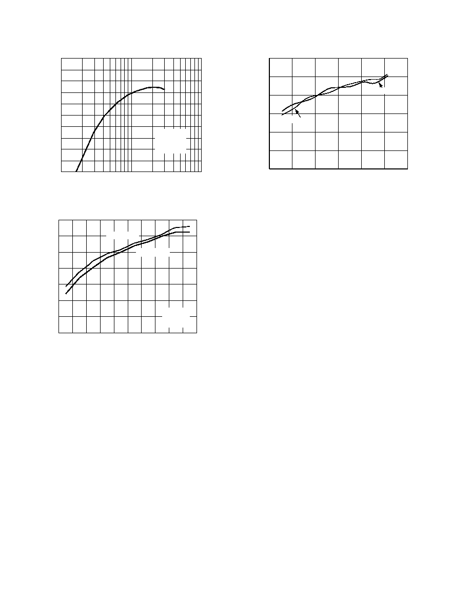
CONVERSION EFFICIENCY (%)
5
6
7
8
9
10
11
12
13
3
TPC 14. Conversion Efficiency vs. Battery Voltage
100
2
V
BAT
(V)
CONVERSION EFFICIENCY (%)
4
6
8
10
12
14
95
90
85
80
75
70
19V
IN
85 C
19V
IN
0 C
TPC 15. Conversion Efficiency vs. Battery Voltage
at Given Temperatures
REV. B
ADP3806
9
THEORY OF OPERATION
The ADP3806 combines a bootstrapped synchronous switching
driver with programmable current control and accurate final
battery voltage control in a constant-current, constant-voltage
(CCCV) Li-Ion battery charger. High accuracy voltage control
is needed to safely charge Li-Ion batteries, which are typically
specified at 4.2 V
± 1% per cell. For a typical notebook computer
battery pack, three or four cells are in series giving a total volt-
age of 12.6 V or 16.8 V. The ADP3806 is available in three
versions, a selectable 12.525 V/16.7 V output, a selectable
12.6 V/16.8 V output, and an adjustable output. The adjustable
output can be programmed for a wide range of battery voltages
using two external precision resistors.
Another requirement for safely charging Li-Ion batteries is
accurate control of the charge current. The actual charge cur-
rent depends on the number of cells in parallel within the
battery pack. Typically, this is in the range of 2 A to 3 A. The
ADP3806 provides flexibility in programming the charge cur-
rent over a wide range. An external resistor is used to sense the
charge current and this voltage is compared to a dc input volt-
age. This programmability allows the current to be changed
during charging. For example, the charge current can be reduced
for trickle charging.
The synchronous driver provides high efficiency when charging at
high currents. Efficiency is important mainly to reduce the amount
of heat generated in the charger but also to stay within the power
limits of the ac adapter. With the addition of a bootstrapped high
side driver, the ADP3806 drives two external power NMOS
transistors for a simple, lower cost power stage.
The ADP3806 also provides an uncommitted current sense
amplifier. This amplifier provides an analog output pin for
monitoring the current through an external sense resistor. The
amplifier can be used anywhere in the system that high side
current sensing is needed.
Charge Current Control
AMP1 in Figure 1 has a differential input to amplify the voltage
drop across an external sense resistor RCS. The input common-
mode range is from ground to VCC, allowing current control in
short circuit and low dropout conditions. The gain of AMP1 is
internally set to 25 V/V for low voltage drop across the sense
resistor. During CC mode, g
m
1 forces the voltage at the output
of AMP1 to be equal to the external voltage at the ISET pin.
By choosing R
CS
and V
ISET
appropriately, a wide range of
charge currents can be programmed.
I
V
R
CHARGE
REF
CS
=
¥
25
(1)
+
SELECT
12.6/16.8
BOOTSTRAPPED
SYNCHRONOUS
DRIVER
VIN
CS+
+
OSCILLATOR
L1
VREF + VREG
UVLO
BIAS
+
CS
R3
249
COMP
REF
2.5V
AGND
BAT
SD
+
CT
SW
REG
6.0V
PGND
VCC
BST
BATTERY
12.6V/16.8V
7.0V
C10
0.1 F
DRVH
DRVL
SYS+
SYS
ISYS
ISET
LOGIC
CONTROL
LC
SYNC
LIMIT
VREF
2.5V
SYSTEM
DC/DC
VREF
ADP3806
1/2 Q1
FD56990A
C15
22 F
C14
2.2 F
**R7
100k
*ADP3806-12.6, ADP3806-12.5: R11 = SHORT, R12 = OPEN;
ADP3806, R11 = 412k , R12 = 102k , R14 = OPEN.
**R7, OPEN IF LC FUNCTION IS NOT USED.
C17
100nF
C7
200pF
C6
180pF
R8
56
C8
0.22 F
*R11
412k
0.1%
*R12
102k
0.1%
R1
2.2
C13
22nF
C16
22 F
C9
100nF
1/2 Q1
FD56990A
22 H
R
CS
40m
R4
249
R5
6.81k
R6
7.5k
R13
10
C2
470nF
C1
470nF
BSTREG
BATSEL
SD
IN DRVLSD
VTH
DRVLSD
*R14
0
R2
2.2
+
AMP2
+
+
+
gm1
gm2
R
SS
10m
AMP1
+
Figure 1. Typical Application
REV. B
10
ADP3806
Typical values of R
CS
range from 25 m
W to 50 mW, and the
input range of ISET is from 0 V to 4 V. If, for example, a 3 A
charger is required, R
CS
could be set to 40 m
W and V
ISET
= 3 V.
The power dissipation in R
CS
should be kept below 500 mW.
In this example, the power is a maximum of 360 mW. Once
R
CS
has been chosen, the charge current can be adjusted during
operation with V
ISET
. Lowering V
ISET
to 125 mV gives a charge
current of 125 mA for trickle charging. Components R3, R4,
and C13 provide high frequency filtering for the current
sense signal.
Final Battery Voltage Control
As the battery approaches its final voltage, the ADP3806 switches
from CC mode to CV mode. The change is achieved by the
common output node of g
m
1 and g
m
2. Only one of the two
outputs controls the voltage at the COMP pin. Both amplifiers
can only pull down on COMP, such that when either amplifier
has a positive differential input voltage, its output is not active.
For example, when the battery voltage, V
BAT
, is low, g
m
2 does
not control V
COMP
. When the battery voltage reaches the desired
final voltage, g
m
2 takes control of the loop, and the charge cur-
rent is reduced.
Amplifier g
m
2 compares the battery voltage to the internal refer-
ence voltage of 2.5 V. In the case of the ADP3806-12.5 and
ADP3806-12.6, an internal resistor divider sets the selectable
final battery voltage.
When BATSEL is high, the final battery voltage is set to three
cells (12.6 V or 12.525 V). BATSEL can be tied to REG for
this state. When BATSEL is tied to ground, V
BAT
equals four
cells (16.8 V or 16.7 V). BATSEL has a 2
mA pull-up current as
a fail-safe to select three cells when it is left open.
The reference and internal resistor divider are referenced to the
AGND pin, which should be connected close to the negative
terminal of the battery to minimize sensing errors.
In contrast, the ADP3806 requires external, precision resistors.
The divider ratio should be set to divide the desired final voltage
down to 2.5 V at the BAT pin
R
R
V
V
BATTERY
11
12
2 5
1
=
.
(2)
These resistors should have a parallel impedance of approximately
80 k
W to minimize bias current errors. When the ADP3806 is in
shutdown, an internal switch disconnects the BAT pin as shown
in Figure 2. This disconnects the resistor, R11, from the battery
and minimizes leakage. The resistance of the internal switch is
less than 200
W.
V
REF
SD
BATTERY
R11
412k
0.1%
ADP3806
R12
102k
0.1%
BAT
BATSEL
g
m
2
Figure 2. Battery Sense Disconnect Circuit
Oscillator and PWM
The oscillator generates a triangle waveform between 1 V and
2.5 V, which is compared to the voltage at the COMP pin,
setting the duty cycle of the driver stage. When V
COMP
is below
1 V, the duty cycle is zero. Above 2.5 V, the duty cycle reaches
its maximum.
MIN
OFF
TIME
BSTREG
BST
DRVH
SW
IN
DRVL
ADP3806
BOOTSTRAPPED
SYNCHRONOUS DRIVER
CBST
PGND
1V
1V
Q1
Q2
DELAY
DRVLSD
SD
DELAY
CMP3
CMP2
CMP1
+
+
+
Figure 3. Bootstrapped Synchronous Driver

REV. B
ADP3806
11
The oscillator frequency is set by the external capacitor at the
CT pin and the internal current source of 150
mA according to
the following formula:
f
A
Cr
V
OSC
=
¥ ¥
150
2 2
1 5
m
.
.
(3)
A 180 pF capacitor sets the frequency to 250 kHz. The frequency
can also be synchronized to an external oscillator by applying a
square wave input on SYNC. The SYNC function is designed
to allow increases only in the oscillator frequency. The f
SYNC
should be no more than 20% higher than f
OSC
. The duty cycle
of the SYNC input is not important and can be anywhere
between 5% and 95%.
7 V Bootstrap Regulator
The driver stage is powered by the internal 7 V bootstrap regu-
lator, which is available at the BSTREG pin. Because the
switching currents are supplied by this regulator, decoupling
must be added. A 0.1
mF capacitor should be placed close to the
ADP3806, with the ground side connected close to the power
ground pin, PGND. This supply is not recommended for use
externally due to high switching noise.
Bootstrapped Synchronous Driver
The PWM comparator controls the state of the synchronous
driver shown in Figure 3. A high output from the PWM com-
parator forces DRVH on and DRVL off. The drivers have an on
resistance of approximately 6
W for fast rise and fall times when
driving external MOSFETs. Furthermore, the bootstrapped
drive allows an external NMOS transistor for the main switch
instead of a PMOS. An external boost diode should be con-
nected between BSTREG and BST, and a boost capacitor of
0.1
mF must be added externally between BST and SW. The
voltage between BST and SW is typically 6.5 V.
The DRVL pin switches between BSTREG and PGND. The 7 V
output of BSTREG drives the external NMOS with high VGS
to lower the on resistance. PGND should be connected close to
the source pin of the external synchronous NMOS. When DRVL
is high, this turns on the lower NMOS and pulls the SW node
to ground. At this point, the boost capacitor is charged up through
the boost diode. When the PWM switches high, DRVL is turned
off and DRVH turns on. DRVH switches between BST and
SW. When DRVH is on, the SW pin is pulled up to the input
supply (typically 16 V), and BST rises above this voltage by
approximately 6.5 V.
Overlap protection is included in the driver to ensure that both
external MOSFETs are not on at the same time. When DRVH
turns off the upper MOSFET, the SW node goes low due to the
inductor current. The ADP3806 monitors the SW voltage, and
DRVL goes high to turn on the lower MOSFET when SW goes
below 1 V. When DRVL turns off, an internal timer adds a
delay of 50 ns before turning DRVH on.
When the charge current is low, the DRVLSD comparator
signals the driver to turn off the low side MOSFET and DRVL
is held low. As shown in Figure 1, the DRVLSD comparator
looks at the output of AMP1. The DRVLSD threshold is set to
1.2 V, corresponding to 48 mV differential voltage between the
CS pins.
The driver stage monitors the voltage across the BST capacitor
with CMP3. When this voltage is less than 4 V, CMP3 forces a
minimum offtime of 200 ns. This ensures that the BST capacitor is
charged even during DRVLSD. However, because a minimum
off time is only forced when needed, the maximum duty cycle is
greater than 99%.
2.5 V Precision Reference
The voltage at the BAT pin is compared to an internal preci-
sion, low temperature drift reference of 2.5 V. The reference is
available externally at the REF pin. This pin should be bypassed
with a 100 pF capacitor to the analog ground pin, AGND. The
reference can be used as a precision voltage externally. How-
ever, the current draw should not be greater than 100
mA, and
noisy, switching type loads should not be connected.
6 V Regulator
The 6 V regulator supplies power to most of the analog circuitry
on the ADP3806. This regulator should be bypassed to AGND
with a 0.1
mF capacitor. This reference has a 3 mA source capa-
bility to power external loads if needed.
LC
The ADP3806 provides a low current (LC) logic output to signal
when the current sense voltage (V
CS
) is below a fixed threshold
and the battery voltage is greater than 95%. LC is an open-drain
output that is pulled low when V
CS
is above the threshold. When
the low current threshold condition is reached, LC is pulled
high by an external resistor to REF or another appropriate pull-up
voltage. To determine when LC goes low, an internal compara-
tor senses when the current falls below 12.5% of full scale (20 mV
across the CS pins). The comparator has hysteresis to prevent
oscillation around the trip point.
To prevent false triggering (such as during soft-start), the com-
parator is only enabled when the battery voltage is within 5% of
its final voltage. As the battery is charging up, the comparator
will not go low even if the current falls below 12.5% as long as
the battery voltage is below 95% of full scale. Once the battery
has risen above 95%, the comparator is enabled. This pin can
be used to indicate the end of the charge process.
System Current Sense
An uncommitted differential amplifier is provided for additional
high side current sensing. This amplifier, AMP2, has a fixed
gain of 50 V/V from the SYS+ and SYS pins to the analog
output at ISYS. ISYS has a 1 mA source capability to drive an
external load. The common-mode range of the input pins is
from 4 V to VCC. This amplifier is the only part of the ADP3806
that remains active during shutdown. The power to this block is
derived from the bias current on the SYS+ and SYS pins.
A separate comparator at the LIMIT pin signals when the voltage
on the ISYS pin exceeds 2.5 V typically. The internal compara-
tor has an open-drain output, which produces the function
shown in the TPC 10 graph of V
LIMIT
versus V
ISYS
. The LIMIT
pin should be externally pulled up to 5 V, 2.5 V, or some other
voltage as needed through a resistor. This graph was taken with
a 50 k
W pull-up resistor to 5 V and to 2.5 V. When ISYS is
below 2.4 V, the LIMIT pin has high output impedance. The
open-drain output is capable of sinking 700
mA when the thresh-
old is exceeded. This comparator is turned off during shutdown
to conserve power.

REV. B
12
ADP3806
Shutdown
A high impedance CMOS logic input is provided to turn off the
ADP3806. When the voltage on
SD is less than 0.8 V, the
ADP3806 is placed in low power shutdown. With the exception
of the system current sense amplifier, AMP2, all other circuitry
is turned off. The reference and regulators are pulled to ground
during shutdown and all switching is stopped. During this state,
the supply current is less than 5
mA. Also, the BAT, CS+, CS,
and SW pins go to high impedance to minimize current drain
from the battery.
UVLO
Undervoltage lock-out, UVLO, is included in the ADP3806 to
ensure proper startup. As VCC rises above 1 V, the reference
and regulators will track VCC until they reach their final volt-
ages. However, the rest of the circuitry is held off by the UVLO
comparator. The UVLO comparator monitors both regulators
to ensure that they are above 5 V before turning on the main
charger circuitry. This occurs when VCC reaches 6 V. Monitor-
ing the regulator outputs makes sure that the charger circuitry
and driver stage have sufficient voltage to operate normally. The
UVLO comparator includes 300 mV of hysteresis to prevent
oscillations near the threshold.
Startup Sequence
During a startup from either
SD going high or VCC exceeding
the UVLO threshold, the ADP3806 initiates a soft-start sequence.
The soft-start timing is set by the compensation capacitor at the
COMP pin and an internal 40
mA source. Initially, both DRVH
and DRVL are held low until VCOMP reaches 1 V. This delay
time is set by
t
C
V
A
DELAY
COMP
=
¥1
40
m
(4)
For a 0.22
mF COMP capacitor, t
DELAY
is 5 ms. After this initial
delay, the duty cycle is very low and then ramps up to its final
value with the same ramp rate given for t
DELAY
. For example, if
V
IN
is 16 V and the battery is 10 V when charging is started, the
duty cycle will be approximately 65%, corresponding to a V
COMP
of ~2 V. The time for the duty cycle to ramp from 0% at V
COMP
= 1 V to 65% at V
COMP
= 2 V is approximately 5 ms. Because
the charge current is equal to zero at first, DRVLSD is active
and DRVL will not turn on. However, if the BST capacitor is
discharged, DRVL will be forced on for a minimum on time
of 200 ns each clock period until the BST capacitor is charged
to greater than 4 V. Typically the BST capacitor is charged in five
to ten clock cycles.
Loop Feed Forward
As the startup sequence discussion shows, the response time at
COMP is slowed by the large compensation capacitor. To speed
up the response, two comparators can quickly feed forward around
the normal control loop and pull the COMP node down to limit
any overshoot in either short-circuit or overvoltage conditions.
The overvoltage comparator has a trip point set to 20% higher
than the final battery voltage. The overcurrent comparator thresh-
old is set to 180 mV across the CS pins, which is 15% above the
maximum programmable threshold. When these comparators
are tripped, a normal soft-start sequence is initiated. The over-
voltage comparator is valuable when the battery is removed
during charging. In this case, the current in the inductor causes
the output voltage to spike up, and the comparator limits the
maximum voltage. Neither of these comparators affects the loop
under normal charging conditions.
APPLICATION INFORMATION
Design Procedure
Refer to Figure 1, the typical application circuit, for the follow-
ing description. The design follows that of a buck converter.
With Li-Ion cells it is important to have a regulator with accu-
rate output voltage control.
Battery Voltage Settings
The ADP3806 has three options for voltage selection:
1. 12.525 V/16.7 V as selectable fixed voltages
2. 12.6 V/16.8 V as selectable fixed voltages
3. Adjustable
When using the fixed versions, R11 should be a short or 0
W
wire jumper and R12 should be an open circuit. When using the
adjustable version, the following equation gives the ratio of the
two resistors:
R
R
V
BAT
11
12
2 5
1
= ÊËÁ
^
¯
~
.
(5)
Often 0.1% resistors are required to maintain the overall accu-
racy budget in the design.
Inductor Selection
Usually the inductor is chosen based on the assumption that the
inductor ripple current is
±15% of the maximum output dc
current at maximum input voltage. As long as the inductor used
has a value close to this, the system should work fine. The final
choice affects the trade-offs between cost, size, and efficiency.
For example, the lower the inductance, the size is smaller but
ripple current is higher. This situation, if taken too far, will lead
to higher ac losses in the core and the windings. Conversely, a
higher inductance results in lower ripple current and smaller
output filter capacitors, but the transient response will be slower.
With these considerations, the required inductance can be
found from
L
V
V
I
D
T
IN, MAX
BAT
MIN
S
1
=
¥
¥
D
(6)
where the maximum input voltage V
IN, MAX
is used with the
minimum duty ratio D
MIN
. The duty ratio is defined as the ratio
of the output voltage to the input voltage, V
BAT
/V
IN
. The ripple
current is found from
DI
I
BAT, MAX
=
¥
0 3
.
(7)
the maximum peak-to-peak ripple is 30%, that is 0.3, and maxi-
mum battery current, I
BAT, MAX
, is used.
For example, with V
IN, MAX
= 19 V, V
BAT
= 12.6 V, I
BAT,MAX
=
3A, and T
S
= 4
ms, the value of L1 is calculated as 18.9 mH.
Choosing the closest standard value gives L1 = 22
mH.
Output Capacitor Selection
An output capacitor is needed in the charger circuit to absorb
the switching frequency ripple current and smooth the output
voltage. The rms value of the output ripple current is given by
I
V
fL
D
D
rms
IN, MAX
=
( )
1 12
1
(8)
The maximum value occurs when the duty cycle is 0.5. Thus
I
V
fL
rms_MAX
IN, MAX
= 0 072
1
.
(9)

REV. B
ADP3806
13
For an input voltage of 19 V and a 22
mH inductance, the maxi-
mum rms current is 0.26 A. A typical 10
mF or 22 mF ceramic
capacitor is a good choice to absorb this current.
Input Capacitor Ripple
As is the case with a normal buck converter, the pulse current at
the input has a high rms component. Therefore, since the input
capacitor has to absorb this current ripple, it must have an
appropriate rms current rating. The maximum input rms cur-
rent is given by
I
P
D V
D
D
D
rms
BAT
IN
=
¥ ¥
¥
( )
h
1
(10)
where
h is the estimated converter efficiency (approximately
90%, 0.9) and P
BAT
is the maximum battery power consumed.
This is a worst-case calculation and, depending on total charge
time, the calculated number could be relaxed. Consult the
capacitor manufacturer for further technical information.
Decoupling the VCC Pin
It is a good idea to use an RC filter (R13 and C14) from the
input voltage to the IC both to filter out switching noise and to
supply bypass to the chip. During layout, this capacitor should
be placed as close to the IC as possible. Values between 0.1
mF
and 2.2
mF are recommended.
Current-Sense Filtering
During normal circuit operation, the current-sense signals can
have high frequency transients that need filtering to ensure
proper operation. In the case of the CS+ and CS inputs, the
resistors (R3 and R4) are set to 249
W while the filter capacitor
(C13) value is 22 nF. For the system current sense circuits,
common-mode filtering from SYS+ and SYS to ground is
needed. 470 nF ceramic capacitors (C1, C2) with 2.2
W resistors
(R1, R2) will often do. These time constants can be adjusted in
the laboratory if required but represent a good starting point.
MOSFET Selection
One of the features of the ADP3806 is that it allows use of a
high side NMOS switch instead of a more costly PMOS device.
The converter also uses synchronous rectification for optimal
efficiency. In order to use a high side NMOS, an internal boot-
strap regulator automatically generates a 7 V supply across C9.
Maximum output current determines the R
DS(ON)
requirement
for the two power MOSFETs. When the ADP3806 is operating
in continuous mode, the simplifying assumption can be made
that one of the two MOSFETs is always conducting the load
current. The power dissipation for each MOSFET is given by:
Upper MOS
P
R
I
D
V
I
D
T
f
DISS
DS ON
BAT
IN
BAT
SW
=
¥
¥
(
)
+
¥
¥
¥
¥
(
)
2
(11)
Lower MOS
P
R
I
D
V
I
D
T
f
DISS
DS ON
BAT
IN
BAT
SW
=
¥
¥
(
)
+
¥
¥
¥
¥
(
)
1
1
2
(12)
where f is the switching frequency and T
SW
is the switch transi-
tion time, usually 10 ns. The first term accounts for conduction
losses while the second term estimates switching losses. Using
these equations and the manufacturer's data sheets, the proper
device can be selected.
A Schottky diode, D1, in parallel with Q2 conducts only during
dead time between the two power MOSFETs. D1's purpose is
to prevent the body diode of the lower N-channel MOSFET
from turning on, which could cost as much as 1% in efficiency.
One option is to use a combined MOSFET with the Schottky
diode in a single package; these integrated packages often work
better in practice. Examples are the IRF7807D2 and the Si4832.
REV. B
14
ADP3806
OUTLINE DIMENSIONS
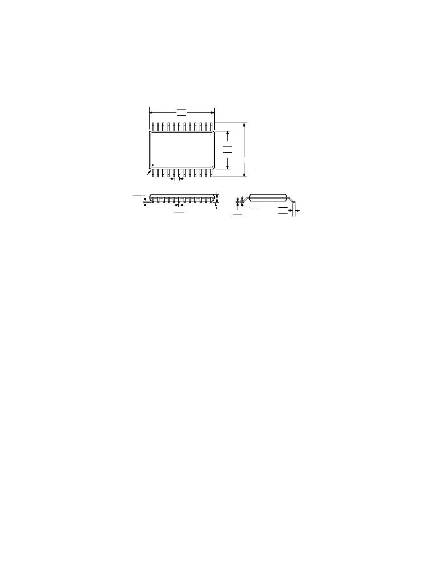
24-Lead Thin Shrink Small Outline Package [TSSOP]
(RU-24)
Dimensions shown in millimeters
24
13
12
1
6.40 BSC
4.50
4.40
4.30
PIN 1
7.90
7.80
7.70
0.15
0.05
0.30
0.19
0.65
BSC
1.20
MAX
0.20
0.09
0.75
0.60
0.45
8
0
SEATING
PLANE
COMPLIANT TO JEDEC STANDARDS MO-153AD
0.10 COPLANARITY

REV. B
ADP3806
15
Revision History
Location
Page
2/04--Data Sheet changed from REV. A to REV. B.
Changes to SPECIFICATIONS . . . . . . . . . . . . . . . . . . . . . . . . . . . . . . . . . . . . . . . . . . . . . . . . . . . . . . . . . . . . . . . . . . . . . . . . . . . . 2
Changes to ORDERING GUIDE . . . . . . . . . . . . . . . . . . . . . . . . . . . . . . . . . . . . . . . . . . . . . . . . . . . . . . . . . . . . . . . . . . . . . . . . . . . 4
Updated OUTLINE DIMENSIONS . . . . . . . . . . . . . . . . . . . . . . . . . . . . . . . . . . . . . . . . . . . . . . . . . . . . . . . . . . . . . . . . . . . . . . . 14
6/03--Data Sheet changed from REV. 0 to REV. A.
Updated SPECIFICATIONS . . . . . . . . . . . . . . . . . . . . . . . . . . . . . . . . . . . . . . . . . . . . . . . . . . . . . . . . . . . . . . . . . . . . . . . . . . . . . . 2
Updated ABSOLUTE MAXIMUM RATINGS . . . . . . . . . . . . . . . . . . . . . . . . . . . . . . . . . . . . . . . . . . . . . . . . . . . . . . . . . . . . . . . . 4
Changes to ORDERING GUIDE . . . . . . . . . . . . . . . . . . . . . . . . . . . . . . . . . . . . . . . . . . . . . . . . . . . . . . . . . . . . . . . . . . . . . . . . . . . 4
Updated OUTLINE DIMENSIONS . . . . . . . . . . . . . . . . . . . . . . . . . . . . . . . . . . . . . . . . . . . . . . . . . . . . . . . . . . . . . . . . . . . . . . . 14

C0261102/04(B)
16
Document Outline
- FEATURES
- APPLICATIONS
- GENERAL DESCRIPTION
- FUNCTIONAL BLOCK DIAGRAM
- SPECIFICATIONS
- ABSOLUTE MAXIMUM RATINGS
- ORDERING GUIDE
- PIN CONFIGURATION
- Typical Performance Characteristics
- THEORY OF OPERATION
- Charge Current Control
- Final Battery Voltage Control
- Oscillator and PWM
- 7 V Bootstrap Regulator
- Bootstrapped Synchronous Driver
- 2.5 V Precision Reference
- 6 V Regulator
- LC
- System Current Sense
- Shutdown
- UVLO
- Startup Sequence
- Loop Feed Forward
- APPLICATION INFORMATION
- Design Procedure
- Battery Voltage Settings
- OUTLINE DIMENSIONS
- Revision History