
Supervisory Circuits with Watchdog and
Manual Reset in 5-Lead SC70 and SOT-23
Preliminary Technical Data
ADM823/ADM824/ADM825
Rev.PrB
Information furnished by Analog Devices is believed to be accurate and reliable.
However, no responsibility is assumed by Analog Devices for its use, nor for any
infringements of patents or other rights of third parties that may result from its use.
Specifications subject to change without notice. No license is granted by implication
or otherwise under any patent or patent rights of Analog Devices. Trademarks and
registered trademarks are the property of their respective owners.
One Technology Way, P.O. Box 9106, Norwood, MA 02062-9106, U.S.A.
Tel: 781.329.4700
www.analog.com
Fax: 781.326.8703
ę 2004 Analog Devices, Inc. All rights reserved.
FEATURES
Precision 2.5 V to 5 V power supply monitor
7 reset threshold options: 2.19 V to 4.63 V
140 ms (min) reset timeout
Watchdog timer with 1.6s timeout (ADM823, ADM824)
Manual reset input (ADM823, ADM825)
Push-pull output stages:
RESET (ADM823)
RESET, RESET (ADM824/ADM825)
Low power consumption (3 ÁA)
Guaranteed reset output valid to V
CC
= 1 V
Power supply glitch immunity
Specified over automotive temperature range
5-lead SC70 and SOT-23 packages
APPLICATIONS
Microprocessor systems
Computers
Controllers
Intelligent instruments
Portable equipment
FUNCTIONAL BLOCK DIAGRAM
ADM823
V
CC
V
CC
MR
GND
WDI
RESET
RESET
GENERATOR
WATCHDOG
DETECTOR
DEBOUNCE
V
REF
04534-0-001
Figure 1.
GENERAL DESCRIPTION
The ADM823/ADM824/ADM825 are supervisory circuits
which monitor power supply voltage levels and code execution
integrity in microprocessor-based systems. As well as providing
power on reset signals, an on-chip watchdog timer can reset the
microprocessor if it fails to strobe within a preset timeout
period. A reset signal can also be asserted by means of an
external push-button, through a manual reset input. The three
parts feature different combinations of watchdog input, manual
reset input and output stage configuration, as shown in Table 1.
Each part is available in a choice of seven reset threshold
options ranging from 2.19 V to 4.63 V. The reset and watchdog
timeout periods are fixed at 140 ms (min) and 1.6s (typ),
respectively.
The ADM823/ADM824/ADM825 are available in 5-lead SC70
and SOT-23 packages and typically consume only 3 ÁA, making
them suitable for use in low power portable applications.
Table 1. Selection Table
Output Stage
Part No.
Watchdog Timer
Manual Reset
RESET
RESET
ADM823 Yes
Yes
Push-Pull ş
ADM824 Yes
ş
Push-Pull Push-Pull
ADM825 ş
Yes
Push-Pull Push-Pull

ADM823/ADM824/ADM825
Preliminary Technical Data
Rev.PrB | Page 2 of 10
TABLE OF CONTENTS
Specifications..................................................................................... 3
Absolute Maximum Ratings............................................................ 5
ESD Caution.................................................................................. 5
Pin Configurations and Function Descriptions ........................... 6
Typical Performance Characteristics ..............................................7
OUTLINE DIMENSIONS ...............................................................9
Ordering Guides......................................................................... 10
Preliminary Technical Data
ADM823/ADM824/ADM825
Rev.PrB | Page 3 of 10
SPECIFICATIONS
V
CC
= 4.75 V to 5.5 V for ADM82_L, V
CC
= 4.5 V to 5.5 V for ADM82_M, V
CC
= 3.15 V to 3.6 V for ADM82_T,
V
CC
= 3 V to 3.6 V for ADM82_S, V
CC
= 2.7 V to 3.6 V for ADM82_R, V
CC
= 2.38 V to 2.75 V for ADM82_Z,
V
CC
= 2.25 V to 2.75 V for ADM82_Y, T
A
= T
MIN
to T
MAX
, unless otherwise noted
Table 2.
Parameter Min
Typ
Max
Unit
Test
Conditions/Comments
SUPPLY
V
CC
Operating Voltage Range
1
5.5
V
T
A
= 0░C to +70░C
1.2
V
T
A
= T
MIN
to T
MAX
Supply
Current
10 24 ÁA WDI and MR unconnected
ADM82_L/M
5
12
ÁA
WDI and MR unconnected
ADM82_T/S/R/Z/Y
RESET THRESHOLD VOLTAGE
ADM82_L
4.56 4.63 4.70 V
T
A
= 25░C
4.50
4.75 V
T
A
= T
MIN
to T
MAX
ADM82_M
4.31 4.38 4.45 V
T
A
= 25░C
4.25
4.50 V
T
A
= T
MIN
to T
MAX
ADM82_T
3.04 3.08 3.11 V
T
A
= 25░C
3.00
3.15 V
T
A
= T
MIN
to T
MAX
ADM82_S
2.89 2.93 2.96 V
T
A
= 25░C
2.85
3.00 V
T
A
= T
MIN
to T
MAX
ADM82_R
2.59 2.63 2.66 V
T
A
= 25░C
2.55
2.70 V
T
A
= T
MIN
to T
MAX
ADM82_Z (SC70 only)
2.28 2.32 2.35 V
T
A
= 25░C
2.25
2.38 V
T
A
= T
MIN
to T
MAX
ADM82_Y (SC70 only)
2.16 2.19 2.22 V
T
A
= 25░C
2.13
2.25 V
T
A
= T
MIN
to T
MAX
RESET THRESHOLD TEMPERATURE COEFFICIENT
40
ppm/░C
RESET
THRESHOLD
HYSTERESIS
10
mV
ADM82_L/M
5
mV
ADM82_T/S/R/Z/Y
RESET
TIMEOUT
PERIOD
140 200 280 ms
V
CC
TO RESET DELAY
40
Ás
V
TH
ş V
CC
= 100 mV
RESET Output Voltage
0.4
V
V
CC
= V
TH
min, I
SINK
= 3.2 mA,
ADM82_L/M
0.3
V
V
CC
= V
TH
min, I
SINK
= 1.2 mA,
ADM82_T/S/R/Z/Y
0.3
V
T
A
= 0░C to 70░C, V
CC
= 1 V,
V
CC
falling, I
SINK
= 50 ÁA
V
CC
- 1.5
V
V
CC
= V
TH
max, I
SOURCE
= 120 ÁA,
ADM82_L/M
0.8 Î V
CC
V
V
CC
= V
TH
max, I
SOURCE
= 30 ÁA,
ADM82_T/S/R/Z/Y
RESET Output Short Circuit Current
800
ÁA
RESET = 0 V, V
CC
= 5.5 V,
ADM82_L/M
400
ÁA
RESET = 0 V, V
CC
= 5.5 V,
ADM82_T/S/R/Z/Y
RESET
Output
Voltage
0.4
V
V
CC
= V
TH
max, I
SINK
= 3.2 mA,
ADM824L/M, ADM825L/M
0.3
V
V
CC
= V
TH
max, I
SINK
= 1.2 mA,
ADM824T/S/R/Z/Y,
ADM825T/S/R/Z/Y
0.8 Î V
CC
V
V
CC
> = 1.8 V, I
SOURCE
= 150 ÁA

ADM823/ADM824/ADM825
Preliminary Technical Data
Rev.PrB | Page 4 of 10
Parameter Min
Typ
Max
Unit
Test
Conditions/Comments
WATCHDOG INPUT (ADM823, ADM824)
Watchdog Timeout Period
1.12
1.6
2.40
s
WDI Pulse Width
50
ns
V
IL
= 0.4 V, V
IH
= 0.8 Î
V
CC
,
WDI
Input
Threshold
V
IL
0.3
Î
V
CC
V
V
IH
0.7 Î V
CC
V
WDI Input Current
120
160
ÁA
V
WDI
= V
CC
, time average
-20 -15
ÁA V
WDI
= 0, time average
MANUAL RESET INPUT (ADM823, ADM825)
MR Input Threshold
0.3
Î
V
CC
V
0.7 Î V
CC
V
MR Input Pulse Width
1
Ás
MR Glitch Rejection
100
ns
MR Pull-up Resistance
35 52 75 k
MR to Reset Delay
500
ns

Preliminary Technical Data
ADM823/ADM824/ADM825
Rev.PrB | Page 5 of 10
ABSOLUTE MAXIMUM RATINGS
T
A
= 25░C, unless otherwise noted.
Table 3.
Parameter
Rating
V
CC
ş0.3 V to +6 V
Output Current (RESET, RESET)
20 mA
Operating Temperature Range
ş40░C to +125░C
Storage Temperature Range
ş65░C to +150░C
JA
Thermal Impedance
SC70 146░C/W
SOT-23 270░C/W
Lead Temperature
Soldering (10 sec)
300░C
Vapor Phase (60 sec)
215░C
Infrared (15 sec)
220░C
Stresses above those listed under Absolute Maximum Ratings
may cause permanent damage to the device. This is a stress
rating only and functional operation of the device at these or
any other conditions above those indicated in the operational
section of this specification is not implied. Exposure to absolute
maximum rating conditions for extended periods may affect
device reliability.
ESD CAUTION
ESD (electrostatic discharge) sensitive device. Electrostatic charges as high as 4000 V readily accumulate on the
human body and test equipment and can discharge without detection. Although this product features
proprietary ESD protection circuitry, permanent damage may occur on devices subjected to high energy
electrostatic discharges. Therefore, proper ESD precautions are recommended to avoid performance
degradation or loss of functionality.

ADM823/ADM824/ADM825
Preliminary Technical Data
Rev.PrB | Page 6 of 10
PIN CONFIGURATIONS AND FUNCTION DESCRIPTIONS
ADM823
TOP VIEW
(Not to Scale)
RESET
1
GND
2
MR
3
V
CC
WDI
5
4
04534-0-002
Figure 2. ADM823 Pin Configuration
ADM824
TOP VIEW
(Not to Scale)
RESET
1
GND
2
RESET
3
V
CC
WDI
5
4
04534-0-003
Figure 3. ADM824 Pin Configuration
ADM825
TOP VIEW
(Not to Scale)
RESET
1
GND
2
RESET
3
V
CC
MR
5
4
04534-0-004
Figure 4. ADM825 Pin Configuration
Table 4. Pin Function Descriptions
Pin. No.
Mnemonic
Description
1
RESET
Push-Pull Active-Low Reset Output. Asserted whenever V
CC
is below the reset threshold, V
TH
.
2 GND
Ground.
3
MR (ADM823)
Manual Reset Input. This is an active-low input which, when forced low for at least 1Ás, generates
a reset. It features a 52 k internal pull-up.
RESET (ADM824/ADM825)
Active-High, Push-Pull Reset Output.
4 WDI
(ADM823/ADM824)
Watchdog Input. Generates a reset if the voltage on the pin remains low or high for the duration
of the watchdog timeout. The timer is cleared if a logic transition occurs on this pin or if a reset is
generated.
MR (ADM825)
Manual Reset Input.
5 V
CC
Power Supply Voltage Being Monitored.
Preliminary Technical Data
ADM823/ADM824/ADM825
Rev.PrB | Page 7 of 10
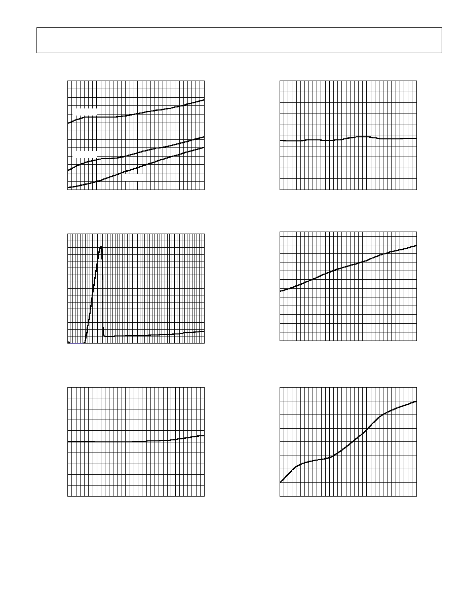
TYPICAL PERFORMANCE CHARACTERISTICS
04534-0-005
TEMPERATURE (░C)
120
ş40
ş20
0
20
40
60
80
100
I
CC
(
Á
A)
10.0
9.0
9.5
8.0
7.5
8.5
7.0
6.5
6.0
5.5
5.0
4.5
4.0
3.5
ADM823L
ADM824Y
ADM825R
Figure 5. Supply Current vs. Temperature
04534-0-006
V
CC
(V)
5.5
0
2.0
1.5
1.0
0.5
2.5
3.0
3.5
4.0
4.5
5.0
I
CC
(
Á
A)
80
70
75
60
55
65
50
45
40
35
30
20
10
25
15
5
0
Figure 6. Supply Current vs. Supply Voltage
04534-0-007
TEMPERATURE (░C)
120
ş40
40
20
0
ş20
60
80
100
N
O
R
M
A
L
IZED
R
ESET TH
R
ESH
OLD
1.05
1.03
1.04
1.01
1.00
1.02
0.99
0.98
0.97
0.96
0.95
Figure 7. Normalized Reset Threshold vs. Temperature
04534-0-008
TEMPERATURE (░C)
120
ş40
40
20
0
ş20
60
80
100
V
CC
TO RESET DELAY (
Á
s)
100
80
90
60
50
70
40
30
20
10
0
Figure 8. Reset Comparator Propagation Delay vs. Temperature (V
CC
Falling)
04534-0-009
TEMPERATURE (░C)
120
ş40
40
20
0
ş20
60
80
100
MANUAL RE
S
E
T
TO RE
S
E
T DE
LAY
(ns
)
340
300
320
260
240
280
220
200
180
160
140
120
100
Figure 9. Manual Reset to Reset Propagation Delay vs. Temperature
(ADM823/ADM825)
04534-0-010
TEMPERATURE (░C)
120
ş40
40
20
0
ş20
60
80
100
R
ESET TIM
E
OU
T
250
230
240
210
200
220
190
180
170
Figure 10. Reset Timeout Period vs. Temperature
ADM823/ADM824/ADM825
Preliminary Technical Data
Rev.PrB | Page 8 of 10
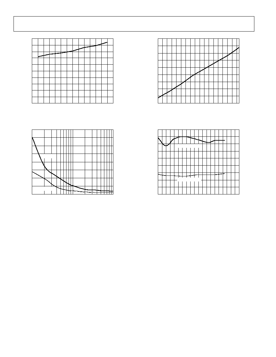
04534-0-011
TEMPERATURE
125
ş40
60
85
25
0
ş20
TIMEOUT PERIOD (s)
2.0
1.6
1.8
1.4
1.2
0.8
1.0
0.6
0.4
0.2
0
Figure 11. Watchdog Timeout Period vs. Temperature
(ADM823/ADM824)
04534-0-012
OVER DRIVE VOD (mV)
1000
10
100
MAX
I
MUM TRANS
IE
NT DURATION (
Á
s)
160
120
140
100
60
80
40
20
0
V
TH
= 4.9V
V
TH
= 2.93V
Figure 12. Maximum V
CC
Transient Duration vs. Reset Threshold Overdrive
04534-0-013
TEMPERATURE (░C)
100
ş50
0
50
MR MINIMUM P
U
LS
E
WIDTH (ns
)
190
160
180
170
150
130
140
120
110
100
Figure 13. Manual Reset Minimum Pulse Width vs. Temperature
(ADM823/ADM825)
04534-0-014
TEMPERATURE (░C)
160
ş40
10
110
60
MINIMUM P
U
LS
E
WIDTH (
n
s
)
3.8
3.2
3.6
3.4
3.0
2.6
2.8
2.4
2.2
2.0
NEGATIVE PULSE
POSITIVE PULSE
Figure 14. Watchdog Input Minimum Pulse Width vs. Temperature
(ADM823/ADM824)
Preliminary Technical Data
ADM823/ADM824/ADM825
Rev.PrB | Page 9 of 10
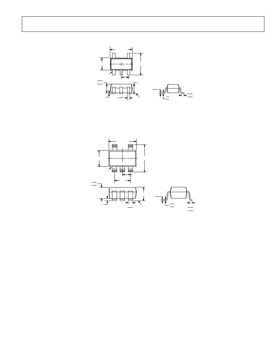
OUTLINE DIMENSIONS
COMPLIANT TO JEDEC STANDARDS MO-203AA
2.00 BSC
0.30
0.15
0.10 MAX
1.00
0.90
0.70
SEATING
PLANE
1.10 MAX
0.22
0.08
0.46
0.36
0.26
3
5
4
1
2
PIN 1
2.10 BSC
0.65 BSC
1.25 BSC
0.10 COPLANARITY
8░
4░
0░
Figure 15. 5-Lead Plastic Surface-Mount Package [SC-70]
(KS-5)
Dimensions shown in millimeters
PIN 1
1.60 BSC
2.80 BSC
1.90
BSC
0.95 BSC
1
3
4
5
2
0.22
0.08
10░
5░
0░
0.50
0.30
0.15 MAX
SEATING
PLANE
1.45 MAX
1.30
1.15
0.90
2.90 BSC
0.60
0.45
0.30
COMPLIANT TO JEDEC STANDARDS MO-178AA
Figure 16. 5-Lead Small Outline Transistor Package [SOT-23]
(RJ-5)
Dimensions shown in millimeters

ADM823/ADM824/ADM825
Preliminary Technical Data
Rev.PrB | Page 10 of 10
ORDERING GUIDES
Table 5. ADM823 Ordering Guide
Table 6. ADM824 Ordering Guide
1
All of the ADM824 models are nonstandard. Contact factory for availability of nonstandard models.
Table 7. ADM825 Ordering Guide
Model
Reset Threshold (V)
Temperature Range Quantity
Package
Type
Branding
ADM823LYKS-R7
4.63
ş40░C to +125░C
3k
SC70-5
N07
ADM823LYRT-R7
4.63
ş40░C to +125░C
3k
SOT-23-5
N07
ADM823MYKS-R7
4.38
ş40░C to +125░C
3k
SC70-5
N07
ADM823MYRT-R7
4.38
ş40░C to +125░C
3k
SOT-23-5
N07
ADM823TYKS-R7
3.08
ş40░C to +125░C
3k
SC70-5
N07
ADM823TYRT-R7
3.08
ş40░C to +125░C
3k
SOT-23-5
N07
ADM823SYKS-R7
2.93
ş40░C to +125░C
3k
SC70-5
N07
ADM823SYRT-R7
2.93
ş40░C to +125░C
3k
SOT-23-5
N07
ADM823RYKS-R7
2.63
ş40░C to +125░C
3k
SC70-5
N07
ADM823RYRT-R7
2.63
ş40░C to +125░C
3k
SOT-23-5
N07
ADM823ZYKS-R7
2.32
ş40░C to +125░C
3k
SC70-5
N07
ADM823YYKS-R7
2.19
ş40░C to +125░C
3k
SC70-5
N07
Model
1
Reset Threshold (V)
Temperature Range
Quantity
Package Type
Branding
ADM824LYKS-R7
4.63
ş40░C to +85░C
3k
SC70-5
N08
ADM824LYRT-R7
4.63
ş40░C to +125░C
3k
SOT-23-5
N08
ADM824MYKS-R7
4.38
ş40░C to +85░C
3k
SC70-5
N08
ADM824MYRT-R7
4.38
ş40░C to +125░C
3k
SOT-23-5
N08
ADM824TYKS-R7
3.08
ş40░C to +85░C
3k
SC70-5
N08
ADM824TYRT-R7
3.08
ş40░C to +125░C
3k
SOT-23-5
N08
ADM824SYKS-R7
2.93
ş40░C to +85░C
3k
SC70-5
N08
ADM824SYRT-R7
2.93
ş40░C to +125░C
3k
SOT-23-5
N08
ADM824RYKS-R7
2.63
ş40░C to +85░C
3k
SC70-5
N08
ADM824RYRT-R7
2.63
ş40░C to +125░C
3k
SOT-23-5
N08
ADM824ZYKS-R7
2.32
ş40░C to +85░C
3k
SC70-5
N08
ADM824YYKS-R7
2.19
ş40░C to +85░C
3k
SC70-5
N08
Model
1
Reset Threshold (V)
Temperature Range Quantity
Package
Type
Branding
ADM825LYKS-R7
4.63
ş40░C to +85░C
3k
SC70-5
N09
ADM825LYRT-R7
4.63
ş40░C to +125░C
3k
SOT-23-5
N09
ADM825MYKS-R7
4.38
ş40░C to +85░C
3k
SC70-5
N09
ADM825MYRT-R7
4.38
ş40░C to +125░C
3k
SOT-23-5
N09
ADM825TYKS-R7
3.08
ş40░C to +85░C
3k
SC70-5
N09
ADM825TYRT-R7
3.08
ş40░C to +125░C
3k
SOT-23-5
N09
ADM825SYKS-R7
2.93
ş40░C to +85░C
3k
SC70-5
N09
ADM825SYRT-R7
2.93
ş40░C to +125░C
3k
SOT-23-5
N09
ADM825RYKS-R7
2.63
ş40░C to +85░C
3k
SC70-5
N09
ADM825RYRT-R7
2.63
ş40░C to +125░C
3k
SOT-23-5
N09
ADM825ZYKS-R7
2.32
ş40░C to +85░C
3k
SC70-5
N09
ADM825YYKS-R7
2.19
ş40░C to +85░C
3k
SC70-5
N09
ę 2004 Analog Devices, Inc. All rights reserved. Trademarks and
registered trademarks are the property of their respective owners.
PR04534-0-6/04(PrB)