Äîêóìåíòàöèÿ è îïèñàíèÿ www.docs.chipfind.ru
High Performance ISM Band
ASK/FSK Transmitter IC
Preliminary Technical Data
ADF7901
Rev. PrD
Information furnished by Analog Devices is believed to be accurate and reliable.
However, no responsibility is assumed by Analog Devices for its use, nor for any
infringements of patents or other rights of third parties that may result from its use.
Specifications subject to change without notice. No license is granted by implication
or otherwise under any patent or patent rights of Analog Devices. Trademarks and
registered trademarks are the property of their respective owners.
One Technology Way, P.O. Box 9106, Norwood, MA 02062-9106, U.S.A.
Tel: 781.329.4700
www.analog.com
Fax: 781.326.8703
© 2005 Analog Devices, Inc. All rights reserved.
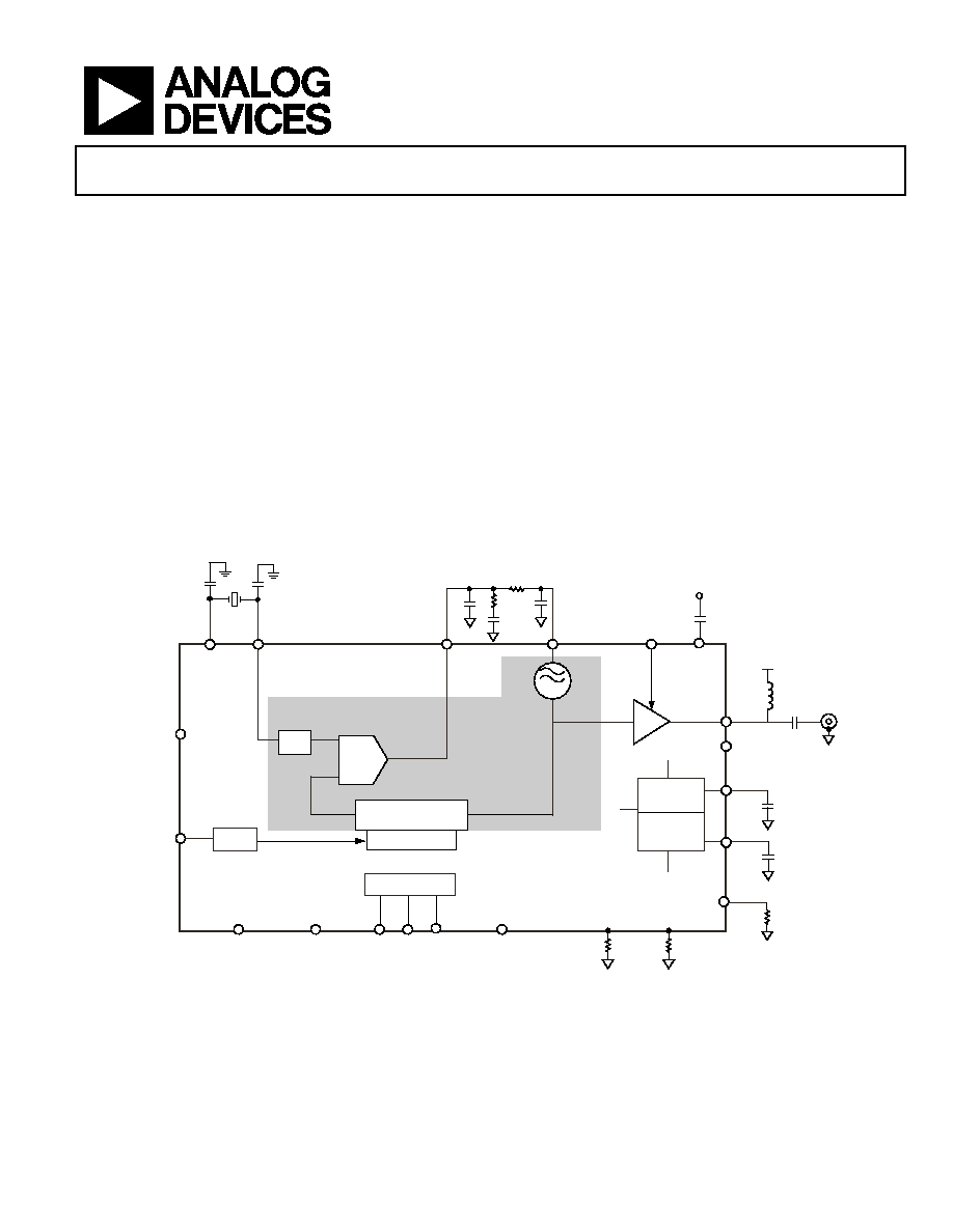
FEATURES
Single chip low power UHF transmitter
369.5 MHz to 395.9 MHz frequency operation using
Fractional-N
PLL and fully integrated VCO
3.0 V supply voltage
Data rates supported < 2.5 kbps
Low current consumption 26 mA at 12 dBm
Output at 384 MHz
Power-down mode (< 1 µA)
24-Lead TSSOP package
GENERAL DESCRIPTION
The ADF7901 is a low power OOK/FSK UHF transmitter
designed for use in RF Remote Control Devices. The device
is capable of Frequency Shift Keying (FSK) modulation on
8 different channels, selectable by 3 external control lines. OOK
modulation is performed by modulating the PA control line.
The on-chip VCO operates at 2 × the output frequency. The
divide by 2 at the output of the VCO reduces the amount of PA
feedthrough. As a result of this, OOK modulation depths of
greater than 50 dB are easily achievable.
The FSK_ADJ and ASK_ADJ resistors can be adjusted in the
system to optimize output power, for each modulation scheme.
An additional 1.5 dB of output power is provided for the lower
bank of channels to adjust for antenna performance. The CE
line allows the transmitter to be powered down completely. In
this mode, the leakage current is typically 0.1 µA.
FUNCTIONAL BLOCK DIAGRAM
R = 1
FSK
DV
DD
T
X
DATA
CE
D
GND
FSK1
OOK_SEL
RF
OUT
RF
GND
V
DD
R
S ET
OSC2
C
VCO
C
REG2
PA_EN
RSET_FSK
RSET_OOK
OSC1
PA
C
REG
2
C
REG1
LDO
REGULATOR
#1
LDO
REGULATOR
#2
PDF
CHARGE
PUMP
÷
FRACTIONAL N
SIGMA-DELTA
FSK2 FSK3
CHANNEL SELECT
VCO
01975-001
Figure 1.

ADF7901
Preliminary Technical Data
Rev. PrD | Page 2 of 12
TABLE OF CONTENTS
Specifications..................................................................................... 3
Absolute Maximum Ratings............................................................ 5
ESD Caution.................................................................................. 5
Pin Configuration and Function Descriptions............................. 6
Typical Performance Characteristics ............................................. 8
Circuit Description........................................................................... 9
Internal Register Settings ............................................................ 9
Loop Filter ..................................................................................... 9
Layout Guidelines....................................................................... 10
Decoupling.............................................................................. 10
Regulator Stability .................................................................. 10
Grounding............................................................................... 10
Supply ...................................................................................... 10
Digital Lines............................................................................ 10
Outline Dimensions ....................................................................... 11
Ordering Guide .......................................................................... 11
REVISION HISTORY
1/05--Revision PrD

Preliminary Technical Data
ADF7901
Rev. PrD | Page 3 of 12
SPECIFICATIONS
V
DD
=3.0 V; GND = 0 V; T
A
= T
MIN
to T
MAX
unless otherwise noted. Typical specifications T
A
= 25°C.
Table 1.
Parameter
1
Min
Typ
Max
Unit
RF
CHARACTERISTICS
Output Frequency Ranges
Channel
1
369.5
MHz
Channel
2
371.1
MHz
Channel
3
375.3
MHz
Channel
4
376.9
MHz
Channel
5
384.0
MHz
Channel
6
388.3
MHz
Channel
7
391.5
MHz
Channel
8
394.3
MHz
Channel
9
395.9
MHz
Phase Frequency Detector Frequency
9.8304
MHz
TRANSMISSION
PARAMETERS
Transmit
Rate
FSK
2
kbps
OOK
2.5
kbps
Frequency Shift Keying
FSK Separation
2
-34.8
kHz, Data = 1
+34.8
kHz, Data = 0
On/Off
Keying
Modulation Depth
3
83
dB, Output Power = 12 dBm
Output
Power
Min/Max Range
4
15
dB
f
OUT
384 MHz
10
12
dBm
f
OUT
> 384 MHz
7
10.5
dBm
Occupied 20 dB BW
OOK at 1 kbits/s
±28
±461.9
kHz
FSK (PA Off/On) at10 Hz
5
±26
±461.9
kHz
LOGIC
INPUTS
V
INH
, Input High Voltage
2.124
V
V
INL
, Input Low Voltage
0.2 × V
DD
V
I
INH
/I
INL
, Input Current
±1
µA
C
IN
, Input Capacitance
10
pF
POWER
SUPPLIES
Voltage
Supply
DV
DD
3.0
V
Transmit Current Consumption
369.5376.9 MHz at +12 dBm
26
mA
384 MHz at +12 dBm
26
mA
388.3395.9 MHz at +10.5 dBm
21
mA
384 MHz at +5 dBm
17
mA
Power-Down
Mode
Low Power Sleep Mode
6
0.2
1
µA
ADF7901
Preliminary Technical Data
Rev. PrD | Page 4 of 12
Parameter
1
Min
Typ
Max
Unit
PHASE-LOCKED
LOOP
VCO Gain
30
MHz/V at 384 MHz
Spurious
7,
3
100 kHz loop BW
Integer Boundary
45
-23
dBc
Reference
-70
-23
dBc
Harmonics
3
Second Harmonic V
DD
= 3.0 V
-24
-21
dBc
Third Harmonic V
DD
= 3.0 V
-14
-11
dBc
All Other Harmonics
-18
dBc
REFERENCE INPUT
Crystal Reference
9.8304
MHz
POWER
AMPLIFIER
PA Output Impedance
97 + 6.4
pF
At
384
MHz
TIMING
INFORMATION
Crystal Oscillator to PLL Lock
3
2
3
ms
PA Enable to PA readyPLL Settle
8
100
250
µs
TEMPERATURE RANGE T
A
0 50
°C
1
Operating temperature range is as follows: 0°C to +50°C.
2
Frequency Deviation = 34 × (9.8304 MHz )/2
14
. Error in the crystal will be reflected in variation in the desired deviation.
3
Not production tested. Based on characterization.
4
The output power can be varied in both ASK/FSK mode by altering the relevant external resistor.
5
Measured using Spectrum Analyzer, 1 MHz span, 100 kHz RBW, MAX HOLD enabled.
6
Maximum power-down current spec applies for the OSC2 pin grounded.
7
Measured > 461.9 kHz away from channel.
8
This spec refers to the time taken for the PLL to regain lock after the PA has been enabled. The PA is should only be enabled after the PLL has settled to the correct
frequency.
Preliminary Technical Data
ADF7901
Rev. PrD | Page 5 of 12
ABSOLUTE MAXIMUM RATINGS
T
A
= 25°C, unless otherwise noted.
Table 2.
Parameter
1
Value
VDD to GND
2
-0.3 V to +4.0 V
RFVDD to GND
-0.3 V to +4.0 V
Digital I/O Voltage to GND
-0.3 V to VDD + 0.3 V
Operating Temperature Range
Industrial (B Version)
0°C to +50°C
Storage Temperature Range
-65°C to +125°C
Maximum Junction Temperature
125°C
TSSOP JA Thermal Impedance
150.4°C/W
Lead Temperature, Soldering
Vapor Phase (60 sec)
235°C
Infrared (15 sec)
240°C
1
This device is a high performance RF integrated circuit with an ESD rating of
<1 kV and it is ESD sensitive. Proper precautions should be taken for
handling and assembly.
2
GND = RFGND = DGND = 0 V.
Stresses above those listed under Absolute Maximum Ratings
may cause permanent damage to the device. This is a stress
rating only; functional operation of the device at these or any
other conditions above those listed in the operational sections
of this specification is not implied. Exposure to absolute
maximum rating conditions for extended periods may affect
device reliability.
ESD CAUTION
ESD (electrostatic discharge) sensitive device. Electrostatic charges as high as 4000 V readily accumulate on the
human body and test equipment and can discharge without detection. Although this product features
proprietary ESD protection circuitry, permanent damage may occur on devices subjected to high energy
electrostatic discharges. Therefore, proper ESD precautions are recommended to avoid performance
degradation or loss of functionality.
ADF7901
Preliminary Technical Data
Rev. PrD | Page 6 of 12
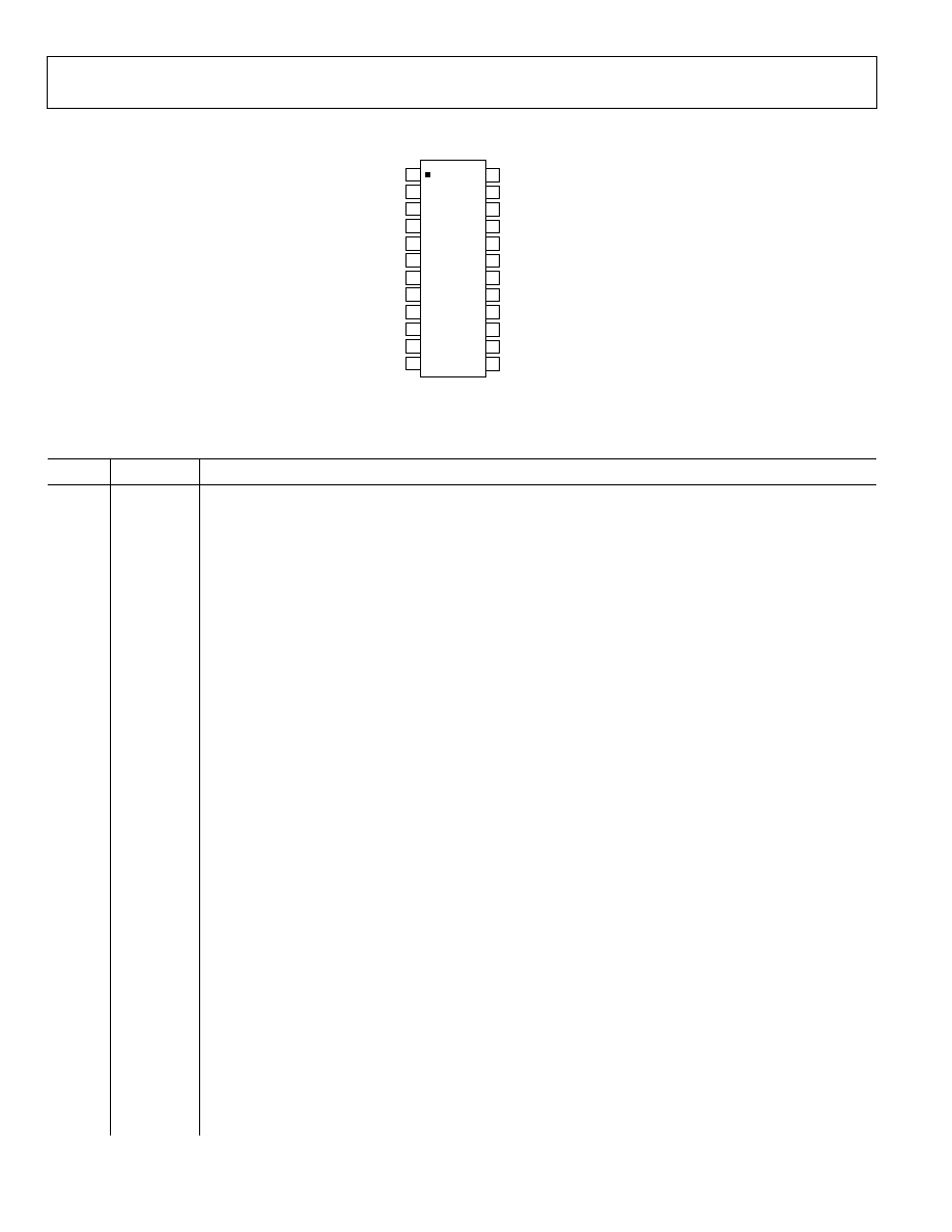
PIN CONFIGURATION AND FUNCTION DESCRIPTIONS
TOP VIEW
(Not to Scale)
24
23
22
21
20
19
18
17
16
15
14
13
1
2
3
4
5
6
7
8
9
10
11
12
ADF7901
D
GND
NC
TxDATA
FSK3
R
SET
CP
OUT
FSK1
CE
OOK_SEL
OSC2
OSC1
RSET_OOK
C
REG1
C
VCO
VCO
IN
DV
DD
RF
GND
RF
OUT
FSK2
DV
DD
PA_EN
C
REG2
D
GND
RSET_FSK
01975-002
Figure 2. Pin Configuration
Table 3. Pin Function Descriptions
Pin No.
Mnemonic
Function
1
DV
DD
Positive Supply for the Digital Circuitry. This must be 3.0 V. Decoupling capacitors to the analog ground plane
should be placed as close as possible to this pin.
2
C
REG1
A 2.2 µF capacitor should be added at C
REG
to reduce regulator noise and improve stability. A reduced capacitor
will improve regulator power-on time but may cause higher spurious.
3
CP
OUT
Charge Pump Output. This output generates current pulses that are integrated in the loop filter. The integrated
current changes the control voltage on the input to the VCO.
4
TxDATA
Digital FSK data to be transmitted is inputted on this pin.
5
D
GND
Ground for Digital Section.
6
NC
No Connect.
7
D
GND
Ground for Digital Section.
8
OSC1
The reference crystal should be connected between this pin and OSC2. The necessary crystal load capacitor
should be tied between this pin and ground.
9
OSC2
The reference crystal should be connected between this pin and OSC1. The necessary crystal load capacitor
should be tied between this pin and ground.
10
OOK_SEL
A high on this pin selects operation in OOK mode at 384 MHz when CE is high.
11
FSK1
FSK Channel Select Pin. This represents the LSB of the channels select pins
12
FSK2
FSK Channel Select Pin.
13
FSK3
FSK Channel Select Pin.
14
CE
Bringing CE low puts the ADF7901 into power-down drawing < 1 µA of current.
15
RSET_OOK
The value of this resistor sets the output power for data = 1 in OOK mode. A resistor of 3.6 k will provide the
maximum output power. Increasing the resistor will reduce the power and the current consumption. A lower
resistor value than 3.6 k can be used to increase the power to a maximum of +14 dBm. The PA will not be
operating efficiently in this mode.
16
RSET_FSK
The value of this resistor sets the output power in FSK mode. A resistor of 3.6 k will provide max output power.
Increasing the resistor will reduce the power and the current consumption. A lower resistor value than 3.6 k can
be used to increase the power to a maximum of +14 dBm. The PA will not be operating efficiently in this mode.
17
C
VCO
A 220 nF capacitor should be tied between C
VCO
and C
REG2
pin. This line should run underneath the ADF7901.
This capacitor is necessary to ensure stable VCO operation.
18
VCO
IN
The tuning voltage on this pin determines the output frequency of the Voltage Controlled Oscillator (VCO).
The higher the tuning voltage the higher the output frequency. The output of the loop filter is connected here.
19
RF
GND
Ground for Output Stage of Transmitter.
20
RF
OUT
The modulated signal is available at this pin. Output power levels are from 5 dBm to +12 dBm. The output
should be impedance matched using suitable components to the desired load.
21
DV
DD
Voltage Supply for VCO, and PA section. This should be supplied with 3.0 V. Decoupling capacitors to the ground

Preliminary Technical Data
ADF7901
Rev. PrD | Page 7 of 12
Pin No.
Mnemonic
Function
plane should be placed as close as possible to this pin.
22
PA_EN
This pin is used to enable the Power Amplifier. This should be modulated with the OOK data in OOK mode. In
FSK mode, it should be enabled when the PLL is locked.
23 R
SET
External resistor to set charge pump current and some internal bias currents. Use 3.6 k as default.
24
C
REG2
A 2.2 µF capacitor should be added at C
REG
to reduce regulator noise and improve stability. A reduced capacitor
will improve regulator power-on time but may cause higher spurious.
ADF7901
Preliminary Technical Data
Rev. PrD | Page 8 of 12
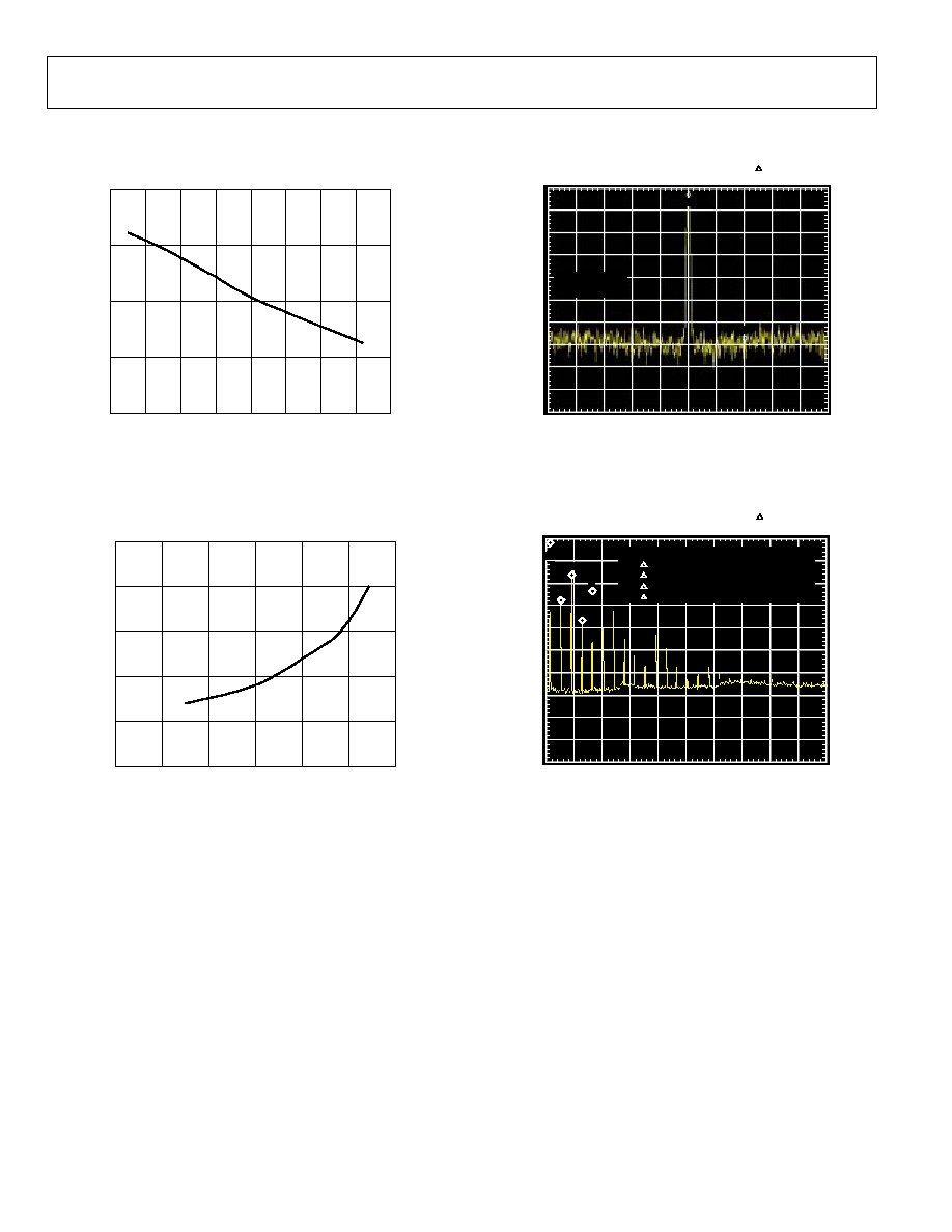
TYPICAL PERFORMANCE CHARACTERISTICS
RSET
OUTP
UT P
O
WE
R (dBm)
16
12
8
4
0
2
3
5
9
7
10
4
6
8
01975-004
Figure 3. Output Power vs. R
SET
FSK, Upper FSK Channels, Measured into 50
OUTPUT POWER (dBm)
I
DD
(mA)
30
25
20
15
10
35
5
9
7
1
4
6
8
01975-005
0
Figure 4. Current Consumption vs. Output Power, Upper FSK Channels,
Measured into 50
Center 395.948 29MHz
#Res BW 300Hz
VBW 300Hz
Span 50kHz
Sweep 2.118 s (601 pts)
Mkr1 10.00kHz
Noise 89.55dB/Hz
Ref 15dBm
Avg
Log
10
dB/
PAvg
W1
S3
£(f):
f<50k
Swp
S2
FS
AA
Atten 30dB
RBW
300.0000000Hz
1R
1
01975-006
Figure 5. Phase Noise at Channel 9
Center 5.50GHz
#Res BW 1MHz
VBW 1MHz
Span 10.5GHz
Sweep 17.52 ms (601 pts)
Mkr4 1.59GHz
21.30dB
Ref 15dBm
Peak
Log
10
dB/
LgAv
Atten 30dB
4R
1
2
3
4
Marker
1
2
3
4
Trace
(1)
(1)
(1)
(1)
Type
Freq
Freq
Freq
Freq
X Axis
400MHz
800MHz
1.19GHz
1.59GHz
Amplitude
25.56dB
13.89dB
34.53dB
21.30dB
01975-007
Figure 6. Harmonic LevelsUp to 4th Harmonic. Measured at Channel 9
in to 50
Preliminary Technical Data
ADF7901
Rev. PrD | Page 9 of 12
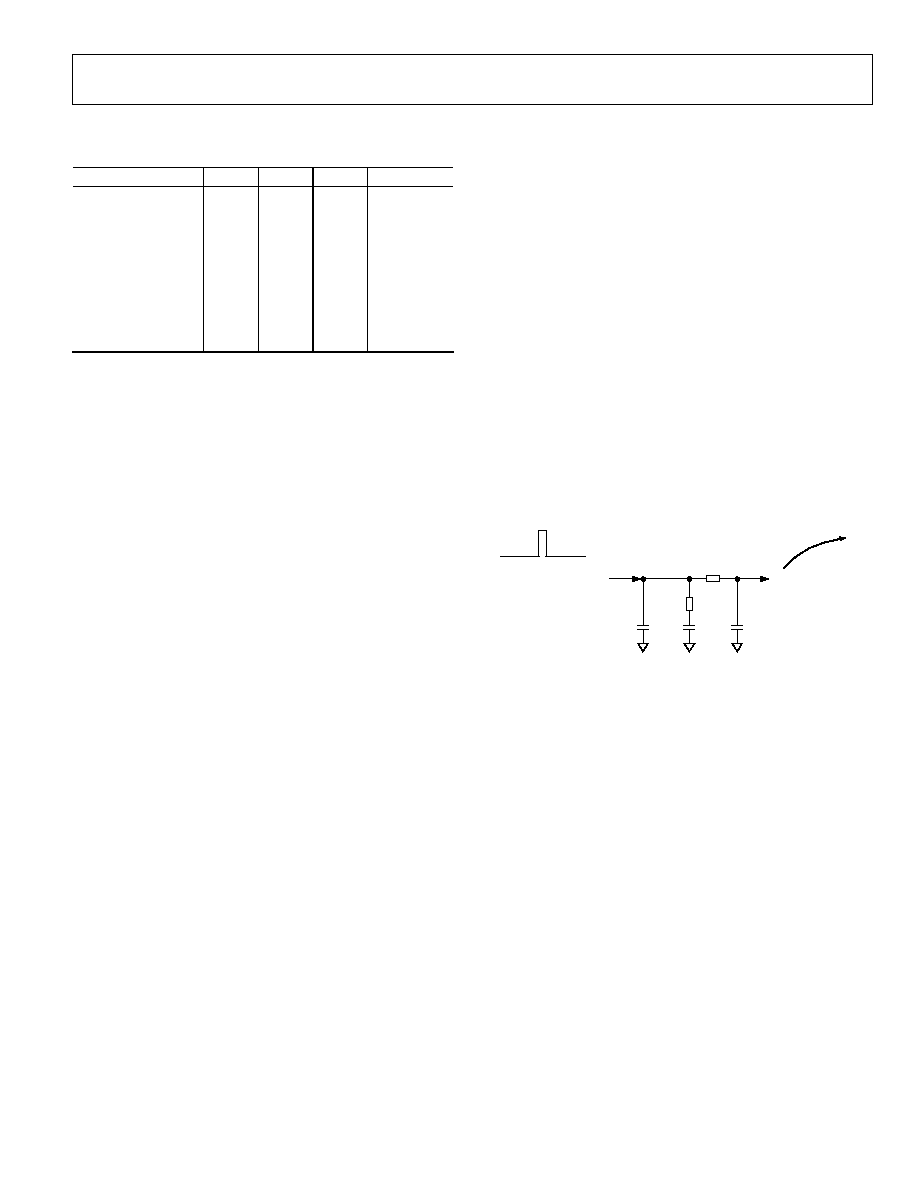
CIRCUIT DESCRIPTION
Table 4.
Frequency
MHz FSK3 FSK2 FSK1 OOK_SEL
369.5
0 0 0 0
371.1
0 0 1 0
375.3
0 1 0 0
376.9
0 1 0 0
384.0
X X X 1
388.3
1 0 0 0
391.5
1 0 1 0
394.3
1 1 0 0
395.9
1 1 1 0
INTERNAL REGISTER SETTINGS
Based on PFD = 9.8304 MHz
REG0
Error Correction 0
R Value 1
XOE 1 (Enabled)
Clock Out 0 (Disabled)
REG1
Ch #1 Integer = 37, Frac = 2406
Ch #2 Integer = 37, Frac = 3073
Ch #3 Integer = 38, Frac = 727
Ch #4 Integer = 38, Frac = 1394
Ch #5(OOK) Integer = 39, Frac = 256
Ch #6 Integer = 39, Frac = 2048
Ch #7 Integer = 39, Frac = 3381
Ch #8 Integer = 40, Frac = 452
Ch #9 Integer = 40, Frac = 1118
VCO Band 1 (Divide-by-2)
LD Precision 1 (Don't care)
REG2
Mod Scheme 0 (FSK)
PA (External R)
Mod Deviation 58 (±35 kHz)
Prescaler 0 (4/5)
REG3
PLL Enable 1
PA Enable (PA_EN Line)
CLKout EN 0 (Off)
Data Invert 0
Charge Pump 1 (3/7)
CP Bleed 0
MuxOut 0
VCOBias 3
PA Bias External R
VCO Band (Switched)
LOOP FILTER
The loop filter integrates the current pulses from the charge
pump to form a voltage that tunes the output of the VCO to the
desired frequency. It also attenuates spurious levels generated by
the PLL. The loop filter design recommended on this design is
300 kHz. This is based on the trade-off between attenuation of
beat note spurious and the need to minimize chirp when the PA
is turned on.
CHARGE
PUMP OUT
VCO
01975-008
Figure 7.
C1 = 680 pF
C2 = 15 nF
C3 = 150 pF
R1 = 120
R2 = 3.3 k
ADF7901
Preliminary Technical Data
Rev. PrD | Page 10 of 12
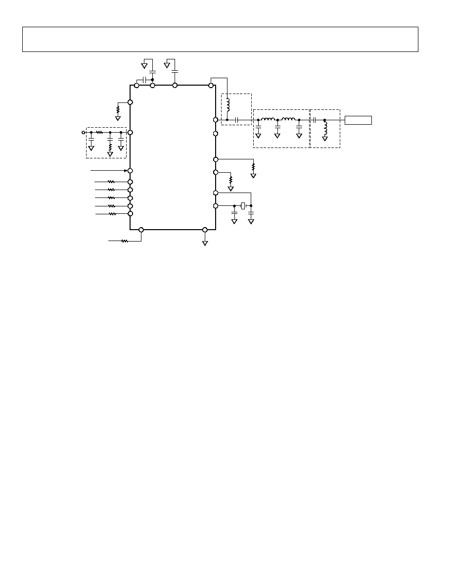
3pF
8pF
22nH
27nH
5.6pF
DVDD
RFOUT
RSET
3.6k
CREG2
2.2mF
220nF
CVCO
CPOUT
VCOIN
VCOIN
FSK1
FSK2
FSK3
OOK_SEL
TxDATA
CE
9.8304MHz
33pF
33pF
GND
OSC2
OSC1
ANTENNA
ADF7901
PA_EN
RSET_FSK
RSET_OOK
3.6k
3.6k
CREG1
2.2mF
3pF
1.5pF
22nH
36nH
MATCHING 50 V
TO ANTENNA
5TH ORDER LOW PASS FILTER
MATCHING RFOUT TO 50V
01975-003
NOTES
1. DECOUPLING CAPACITORS HAVE
BEEN OMITTED FOR CLARITY.
Figure 8. Applications Diagram for the ADF7901 in a Remote Control System
LAYOUT GUIDELINES
The layout of the board is crucial to ensuring low levels of
spurious and harmonics.
Decoupling
Decoupling capacitors (high frequency 22 pF, low frequency
100 nF) should be placed as close as possible to the supply pins
on the part. Low size 0402 and 0603 components are recom-
mended for the high frequency rejection on the supply.
Regulator Stability
A minimum of 1 µF is needed on both C
REG1
and C
REG2
to ensure
stability. An additional 22 pF capacitor can be added to reject
higher frequency noise. Since many of the internal block run off
the regulator it is critical to reduce the noise on this. Low size
0402 and 0603 components are recommended for the high
frequency rejection on the supply.
Grounding
Emphasis should be placed on the grounding once the
decoupling capacitors have been added. The PA stage switches
currents of 15 mA in max power mode. This will cause changes
in the ground resulting in large return currents which can
radiate to other parts of the board. The shortest and least
obstructed ground from RFGND back to the ground of the
battery should be ensured. A 4-layer board will help, as well as
flooding of the top layer. The ground paths should not have any
vias, and should be wide tracks.
Supply
The supply tracks can be routed through vias, as these act as
free inductors on the board and make layout easier on a 2-layer
board. See the Decoupling section. Tracks should be wide.
Digital Lines
Any digital lines should contain a large resistor in series. This
impedance will block signals of many frequencies including
harmonics and the carrier frequency. Long control lines can act
as an antenna. It can be useful to add capacitance to ground.
There will be some capacitance to ground provided by the lines,
and at the input of the digital pins.
Preliminary Technical Data
ADF7901
Rev. PrD | Page 11 of 12
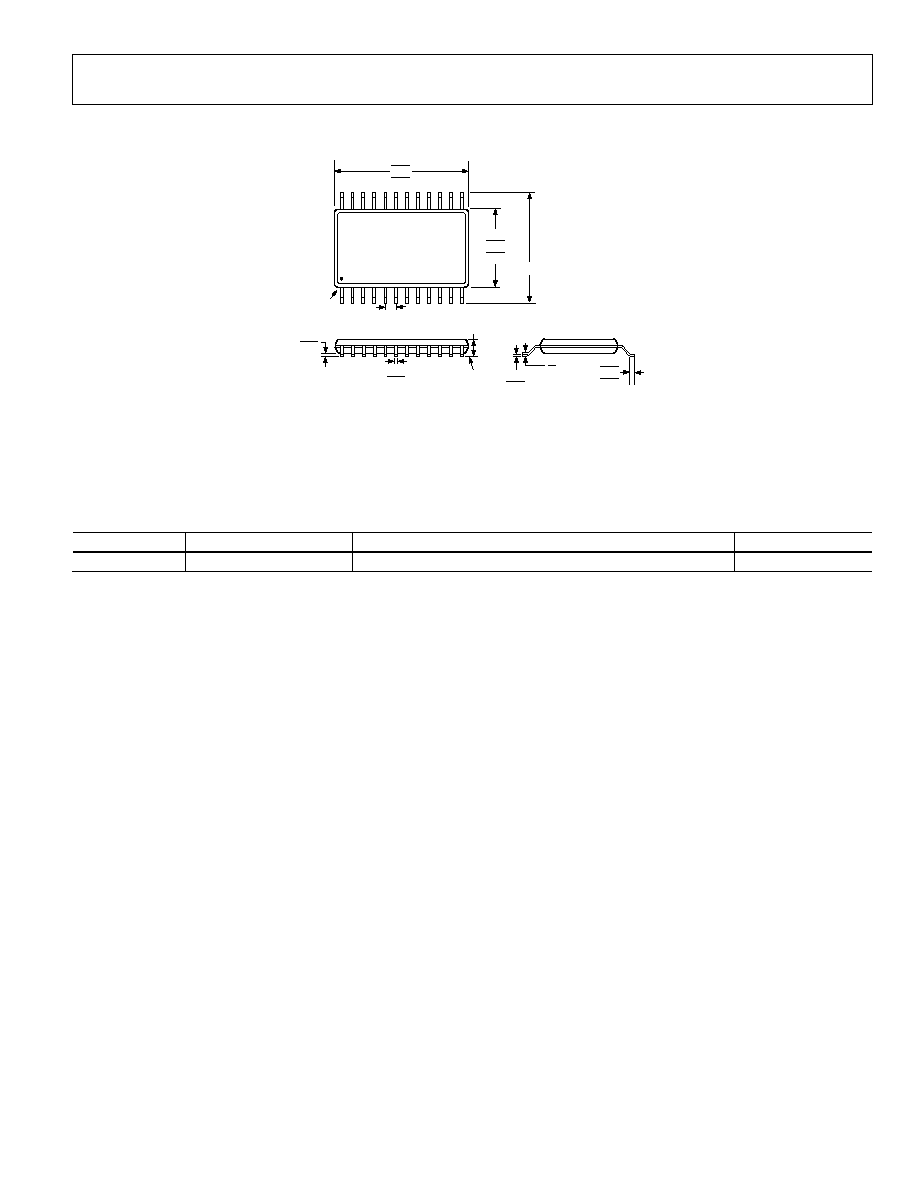
OUTLINE DIMENSIONS
24
13
12
1
6.40 BSC
4.50
4.40
4.30
PIN 1
7.90
7.80
7.70
0.15
0.05
0.30
0.19
0.65
BSC
1.20
MAX
0.20
0.09
0.75
0.60
0.45
8°
0°
SEATING
PLANE
0.10 COPLANARITY
COMPLIANT TO JEDEC STANDARDS MO-153AD
Figure 9. 24-Lead Thin Shrink Small Outline Package [TSSOP]
(RU-24)
Dimensions shown in millimeters
ORDERING GUIDE
Model
Temperature Range
Package Description
Package Option
ADF7901BRU
0°C to +50°C
24-Lead Thin Shrink Small Outline Pacakage [TSSOP]
RU-24

ADF7901
Preliminary Technical Data
Rev. PrD | Page 12 of 12
NOTES
© 2005 Analog Devices, Inc. All rights reserved. Trademarks and
registered trademarks are the property of their respective owners.
PR0534901/05(PrD)
Document Outline
- FEATURES
- GENERAL DESCRIPTION
- FUNCTIONAL BLOCK DIAGRAM
- þÿ
- þÿ
- þÿ
- þÿ
- þÿ
- þÿ