Äîêóìåíòàöèÿ è îïèñàíèÿ www.docs.chipfind.ru
REV. PrB 08/01
Preliminary Technical Data
PRELIMINARY TECHNICAL DATA
Information furnished by Analog Devices is believed to be accurate and
reliable. However, no responsibility is assumed by Analog Devices for its
use, nor for any infringements of patents or other rights of third parties
which may result from its use. No license is granted by implication or
otherwise under any patent or patent rights of Analog Devices.
=
ADE77
52
*
One Technology Way, P.O. Box 9106, Norwood, MA 02062-9106, U.S.A.
Tel: 781/329-4700
World Wide Web Site: http://www.analog.com
Fax: 781/326-8703
© Analog Devices, Inc., 1999
Three Phase Energy Metering IC
with Pulse Output
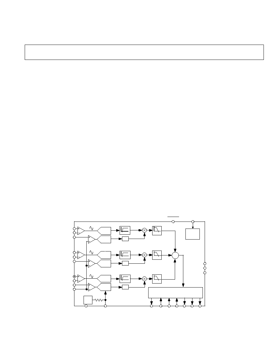
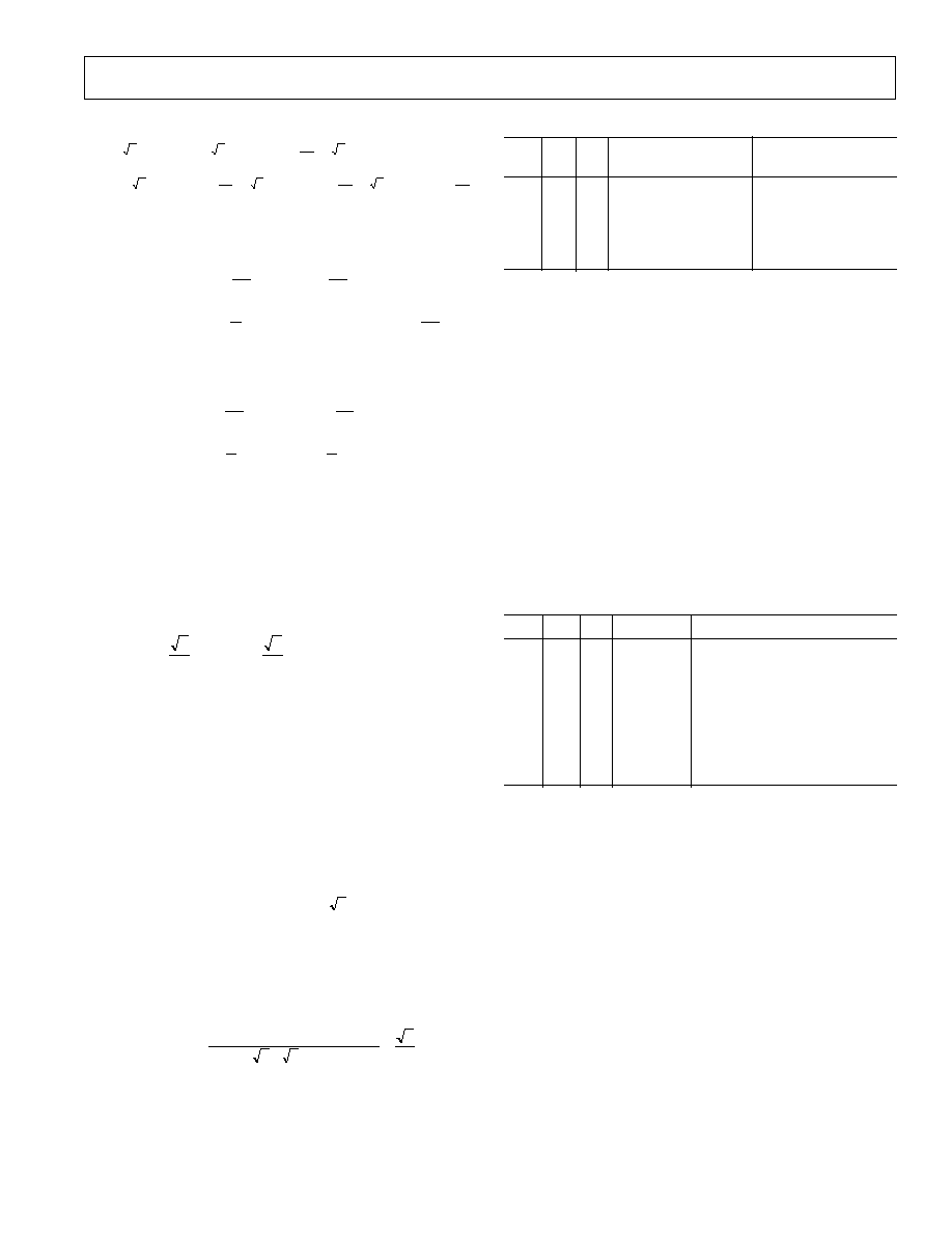
FUNCTIONAL BLOCK DIAGRAM
CLKOUT
CLKIN
DGND
CF
S1
F1
F2
DIGITAL-TO-FREQUENCY
CONVERTER
2.5V
REF
REF
IN/OUT
AGND
4k
IBP
IBN
ADC
VBP
ADC
VN
ICP
ICN
ADC
VCP
ADC
VDD
RESET
ADE7752
Power
Supply
Monitor
HPF
LPF
IAP
IAN
ADC
VAP
ADC
PHASE
CORRECTION
HPF
LPF
PHASE
CORRECTION
HPF
LPF
PHASE
CORRECTION
S0
SCF
REVP
7
8
15
10
14
13
5
6
16
11
12
4
18
21
22
23
24
1
20
19
2
17
3
FEATURES
High Accuracy, Supports 50 Hz/60 Hz IEC 687/1036
Less than 0.1% Error Over a Dynamic Range of
500 to 1
Compatible with 3-phase/3-wire and 3-phase/4-wire
configurations
The ADE7752 Supplies Average Real Power on the
Frequency Outputs F1 and F2
The High Frequency Output CF Is Intended for
Calibration and Supplies
Instantaneous Real Power
The Logic Output REVP indicates a Potential Miswiring or
Negative Power for each phase
Direct Drive for Electromechanical Counters and
Two Phase Stepper Motors (F1 and F2)
Proprietary ADCs and DSP Provide High Accuracy over
Large Variations in Environmental Conditions and
Time
On-Chip Power Supply Monitoring
On-Chip Creep Protection (No Load Threshold)
On-Chip Reference 2.5 V ± 8% (30 ppm/8C Typical)
with External Overdrive Capability
Single 5 V Supply, Low Power (15 mW Typical)
Low Cost CMOS Process
*Patents pending
GENERAL DESCRIPTION
The ADE7752 is a high accuracy three phase electrical
energy measurement IC. The part specifications surpass the
accuracy requirements as quoted in the IEC1036 standard.
The only analog circuitry used in the ADE7752 is in the
ADCs and reference circuit. All other signal processing (e.g.,
multiplication, filtering and summation) is carried out in the
digital domain. This approach provides superior stability and
accuracy over extremes in environmental conditions and over
time.
The ADE7752 supplies average real power information on
the low frequency outputs F1 and F2. These logic outputs
may be used to directly drive an electromechanical counter or
interface with an MCU. The CF logic output gives instan-
taneous real power information. This output is intended to be
used for calibration purposes, or as interface with an MCU.
The ADE7752 includes a power supply monitoring circuit
on the AV
DD
supply pin. The ADE7752 will remain inactive
until the supply voltage on V
DD
reaches 4 V. If the supply falls
below 4 V, the ADE7752 will also be reset and no pulses will
be issued on F1, F2 and CF.
Internal phase matching circuitry ensures that the voltage and
current channels are phase matched. An internal no-load
threshold ensures that the ADE7752 does not exhibit any
creep when there is no load.
The ADE7752 is available in 24-lead SOIC packages.

REV. PrB 08/01
PRELIMINARY TECHNICAL DATA
2
ADE7752SPECIFICATIONS
(V
DD
= 5 V 5%, AGND = DGND = 0 V, On-Chip Reference, CLKIN = 10 MHz,
T
MIN
to T
MAX
= 40 C to +85 C)
Parameter
Units
Test Conditions/Comments
ACCURACY
1, 2
Measurement Error
1
on Current Channel
Voltage Channel with Full-Scale Signal (±500 mV),
+25°C
0.1
% Reading typ
Over a Dynamic Range 500 to 1
Phase Error
1
Between Channels
Line Frequency = 45 Hz to 65 Hz
(PF = 0.8 Capacitive)
±0.1
Degrees(°) max
(PF = 0.5 Inductive)
±0.1
Degrees(°) max
AC Power Supply Rejection
1
S0 = S1 = 1
Output Frequency Variation (CF)
0.01
% Reading typ
V1 = 100 mV rms, V2 = 100 mV rms, @ 50 Hz
Ripple on V
DD
of 200 mV rms @ 100 Hz
DC Power Supply Rejection
1
S0 = S1 = 1
Output Frequency Variation (CF)
0.01
% Reading typ
V1 = 100 mV rms, V2 = 100 mV rms,
V
DD
= 5 V ± 250 mV
ANALOG INPUTS
See Analog Inputs Section
Maximum Signal Levels
±0.125
V max
VAP, VBP, VCP, VN, IAP, IAN, IBP, IBN, ICP and
ICN to AGND
Input Impedance (DC)
400
k
min
CLKIN = 10 MHz
Bandwidth (3 dB)
TBD
kHz typ
CLKIN/256, CLKIN = 10 MHz
ADC Offset Error
1, 2
±15
mV max
See Terminology and
Gain Error
1
±4
% Ideal typ
External 2.5 V Reference,
V1 = 125 mV dc, V2 = 125 mV dc
Gain Error Match
1
±0.2
% Ideal typ
External 2.5 V Reference
REFERENCE INPUT
REF
IN/OUT
Input Voltage Range
2.7
V max
2.5 V + 8%
2.3
V min
2.5 V 8%
Input Impedance
3.7
k
min
Input Capacitance
10
pF max
ON-CHIP REFERENCE
Nominal 2.5 V
Reference Error
±200
mV max
Temperature Coefficient
30
ppm/°C typ
CLKIN
Note All Specifications for CLKIN of 10 MHz
Input Clock Frequency
15
MHz max
5
MHz min
LOGIC INPUTS
3
SCF, S0, S1, and
4-5-6
Input High Voltage, V
INH
2.4
V min
V
DD
= 5 V ± 5%
Input Low Voltage, V
INL
0.8
V max
V
DD
= 5 V ± 5%
Input Current, I
IN
±3
µA max
Typically 10 nA, V
IN
= 0 V to V
DD
Input Capacitance, C
IN
10
pF max
LOGIC OUTPUTS
3
F1 and F2
Output High Voltage, V
OH
I
SOURCE
= 10 mA
4.5
V min
V
DD
= 5 V
Output Low Voltage, V
OL
I
SINK
= 10 mA
0.5
V max
V
DD
= 5 V
CF and REVP
Output High Voltage, V
OH
4
V min
V
DD
= 5 V, I
SOURCE
= 5 mA
Output Low Voltage, V
OL
0.5
V max
V
DD
= 5 V, I
SINK
= 5 mA
POWER SUPPLY
For Specified Performance
V
DD
4.75
V min
5 V 5%
5.25
V max
5 V + 5%
I
DD
4
mA typ
NOTES
1
See Terminology Section for explanation of specifications.
2
See Plots in Typical Performance Graphs.
3
Sample tested during initial release and after any redesign or process change that may affect this parameter.
Specifications subject to change without notice.
REV. PrB 08/01
PRELIMINARY TECHNICAL DATA
3
ADE7752
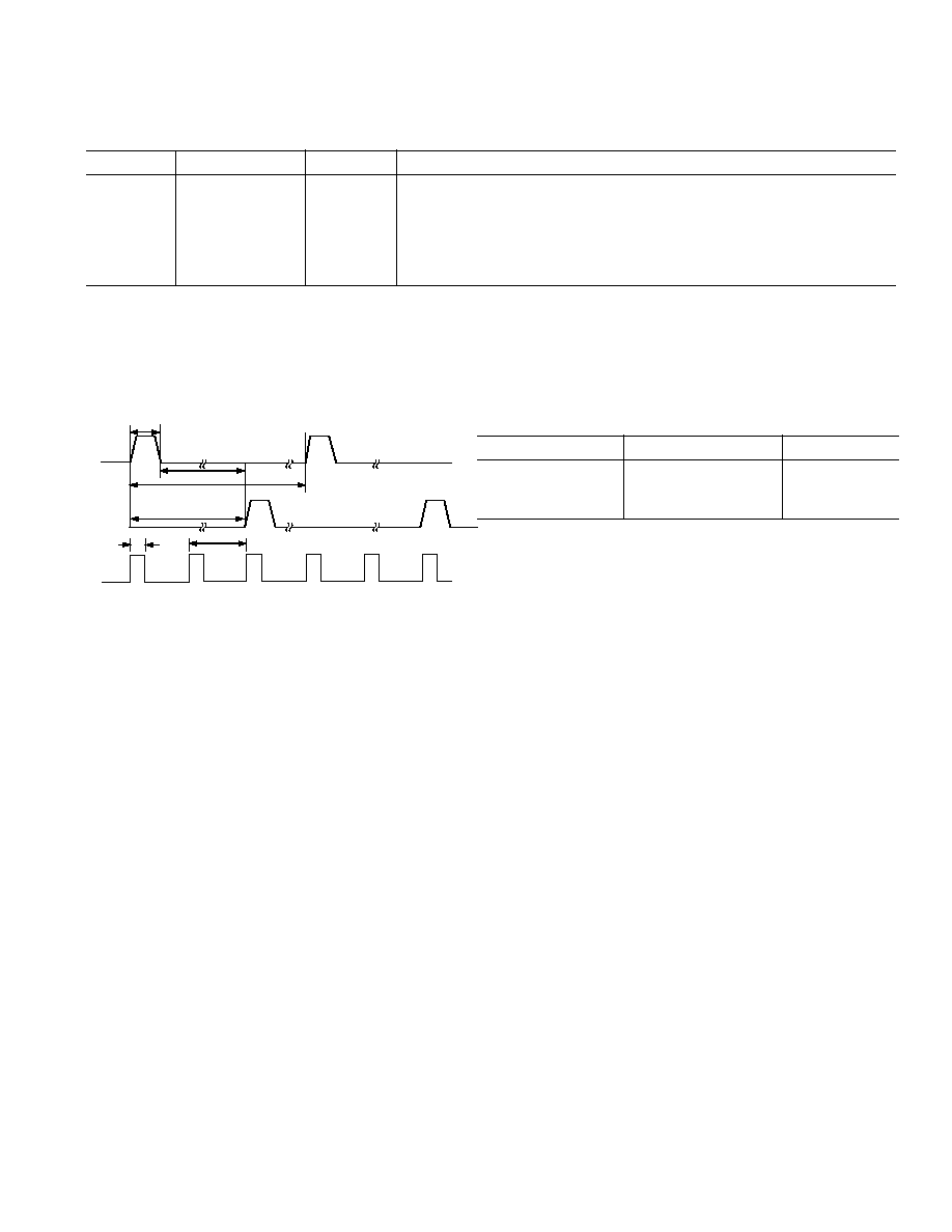
TIMING CHARACTERISTICS
1, 2
Parameter
Units
Test Conditions/Comments
t
1
3
275
ms
F1 and F2 Pulsewidth (Logic High)
t
2
See Table III
sec
Output Pulse Period. See Transfer Function Section
t
3
1/2 t
2
sec
Time Between F1 Falling Edge and F2 Falling Edge
t
4
3, 4
90
ms
CF Pulsewidth (Logic High)
t
5
See Table IV
sec
CF Pulse Period. See Transfer Function Section
t
6
CLKIN/4
sec
Minimum Time Between F1 and F2 Pulse
NOTES
1
Sample tested during initial release and after any redesign or process change that may affect this parameter.
2
See Figure 1.
3
The pulsewidths of F1, F2 and CF are not fixed for higher output frequencies. See Frequency Outputs Section.
4
The CF pulse is always 1 µs in the high frequency mode. See Frequency Outputs section and Table IV.
Specifications subject to change without notice.
ORDERING GUIDE
Model
Package Description
Package Option
ADE7752AR
SOIC Package
R-24
EVAL-ADE7752EB ADE7752 Evaluation
Board
(V
DD
= 5 V 5%, AGND = DGND = 0 V, On-Chip Reference, CLKIN = 10 MHz,
T
MIN
to T
MAX
= 40 C to +85 C)
F1
F2
CF
t1
t6
t2
t3
t4
t5
Figure 1. Timing Diagram for Frequency Outputs

REV. PrB 08/01
PRELIMINARY TECHNICAL DATA
ADE7752
4
ABSOLUTE MAXIMUM RATINGS*
(T
A
= +25°C unless otherwise noted)
V
DD
to AGND . . . . . . . . . . . . . . . . . . . . . . 0.3 V to +7 V
V
DD
to DGND . . . . . . . . . . . . . . . . . . . . . . 0.3 V to +7 V
Analog Input Voltage to AGND
VAP, VBP, VCP, VN, IAP, IAN, . . . . . . . . . . . . . . . . . .
IBP, IBN, ICP and ICN . . . . . . . . . . . . . 6 V to +6 V
Reference Input Voltage to AGND 0.3 V to V
DD
+ 0.3 V
Digital Input Voltage to DGND . 0.3 V to V
DD
+ 0.3 V
Digital Output Voltage to DGND 0.3 V to V
DD
+ 0.3 V
Operating Temperature Range
Industrial . . . . . . . . . . . . . . . . . . . . . . . 40°C to +85°C
Storage Temperature Range . . . . . . . . 65°C to +150°C
Junction Temperature . . . . . . . . . . . . . . . . . . . . . . +150°C
C A U T I O N
ESD (electrostatic discharge) sensitive device. Electrostatic charges as high as 4000 V readily
accumulate on the human body and test equipment and can discharge without detection.
Although the ADE7752 features proprietary ESD protection circuitry, permanent damage may occur
on devices subjected to high energy electrostatic discharges. Therefore, proper ESD precautions are
recommended to avoid performance degradation or loss of functionality.
WARNING!
ESD SENSITIVE DEVICE
24-Lead SOIC, Power Dissipation . . . . . . . . . TBD mW
JA
Thermal Impedance . . . . . . . . . . . . . . . . . . 250 °C/W
Lead Temperature, Soldering
Vapor Phase (60 sec) . . . . . . . . . . . . . . . . . . . +215°C
Infrared (15 sec) . . . . . . . . . . . . . . . . . . . . . . +220°C
*Stresses above those listed under Absolute Maximum Ratings may cause permanent
damage to the device. This is a stress rating only; functional operation of the device
at these or any other conditions above those listed in the operational sections of this
specification is not implied. Exposure to absolute maximum rating conditions for
extended periods may affect device reliability.
TERMINOLOGY
MEASUREMENT ERROR
The error associated with the energy measurement made by
the ADE7752 is defined by the following formula:
%
100
Energy
True
ADE7752
the
by
Registered
Energy
×
=
Energy
True
Error
Percentage
PHASE ERROR BETWEEN CHANNELS
The HPF (High Pass Filter) in the current channel has a
phase lead response. To offset this phase response and
equalize the phase response between channels a phase correc-
tion network is also placed in the current channel. The phase
correction network ensures a phase match between the
current channels and voltage channels to within ±0.1° over a
range of 45Hz to 65Hz and ±0.2° over a range 40Hz to 1kHz.
This phase mismatch between the voltage and the current
channels can be further reduced with the phase calibration
register in each phase.
See Figures 18 and 19.
POWER SUPPLY REJECTION
This quantifies the ADE7752 measurement error as a per-
centage of reading when the power supplies are varied.
For the ac PSR measurement a reading at nominal supplies
(5 V) is taken. A 200 mV rms/100 Hz signal is then
introduced onto the supplies and a second reading obtained
under the same input signal levels. Any error introduced is
expressed as a percentage of reading--see Measurement Error
definition.
For the dc PSR measurement a reading at nominal supplies
(5 V) is taken. The supply is then varied ±5% and a second
reading is obtained with the same input signal levels. Any
error introduced is again expressed as a percentage of
reading.
ADC OFFSET ERROR
This refers to the dc offset associated with the analog inputs
to the ADCs. It means that with the analog inputs connected
to AGND the ADCs still see an analog input signal of 1 mV
to 10 mV, depending on gain setting. However, as the HPF
is always present, the offset is removed from the current
channel and the power calculation is not affected by this
offset.
GAIN ERROR
The gain error of the ADE7752 is defined as the difference
between the measured output frequency (minus the offset) and
the ideal output frequency. The difference is expressed as a
percentage of the ideal frequency. The ideal frequency is
obtained from the ADE7752 transfer function--see Transfer
Function section.

REV. PrB 08/01
5
PRELIMINARY TECHNICAL DATA
ADE7752
PIN FUNCTION DESCRIPTION
Pin No.
MNEMONIC
DESCRIPTION
1
C F
Calibration Frequency Logic Output. The CF logic output gives instantaneous real
power information. This output is intended to be used for calibration purposes. Also see
SCF pin description.
2
D G N D
This provides the ground reference for the digital circuitry in the ADE7752, i.e. multi-
plier, filters and digital-to-frequency converter. Because the digital return currents in
the ADE7752 are small, it is acceptable to connect this pin to the analog ground plane
of the whole system - see Applications Information. However high bus capacitance on the
DOUT pin may result in noisy digital current which could affect performance.
3
V
DD
Power supply. This pin provides the supply voltage for the digital circuitry in the
ADE7752. The supply voltage should be maintained at 5V ± 5% for specified opera-
tion. This pin should be decoupled to DGND with a 10µF capacitor in parallel with a
ceramic 100nF capacitor.
4
REVP
This logic output will go logic high when negative power is detected on any of the three
phase inputs, i.e., when the phase angle between the voltage and the current signals is
greater that 90°. This output is not latched and will be reset when positive power is
once again detected. The output will go high or low at the same time as a pulse is is-
sued on CF.
5,6;
I
AP
, I
AN
;
Analog inputs for current channel. This channel is intended for use with the current
7,8;
I
BP
, I
BN
;
transducer and is referenced in this document as the current channel. These inputs are
9,10
I
CP
, I
CN
fully differential voltage inputs with maximum differential input signal levels of
±0.125V -See Analog Inputs. Both inputs have internal ESD protection circuitry, and in
addition an overvoltage of ±6V can be sustained on these inputs without risk of perma
nent damage.
11
A G N D
This pin provides the ground reference for the analog circuitry in the ADE7754, i.e.
ADCs, temperature sensor, and reference. This pin should be tied to the analog ground
plane or the quietest ground reference in the system. This quiet ground reference
should be used for all analog circuitry, e.g. anti aliasing filters, current and voltage
transducers etc. In order to keep ground noise around the ADE7754 to a minimum, the
quiet ground plane should only connected to the digital ground plane at one point. It is
acceptable to place the entire device on the analog ground plane - see Applications Informa-
tion.
12
REF
IN/OUT
This pin provides access to the on-chip voltage reference. The on-chip reference has a
nominal value of 2.5V ± 8% and a typical temperature coefficient of 30ppm/°C. An
external reference source may also be connected at this pin. In either case this pin
should be decoupled to AGND with a 1µF ceramic capacitor.
13-16
V
N
,V
CP
,
Analog inputs for the voltage channel. This channel is intended for use with the voltage
V
BP
, V
AP
transducer and is referenced as the voltage channel in this document. These inputs are
single-ended voltage inputs with maximum signal level of ±0.125V with respect to V
N
for specified operation. All inputs have internal ESD protection circuitry, and in addi
tion an over voltage of ±6V can be sustained on these inputs without risk of permanent
damage.
17
R E S E T
Reset pin for the ADE7752. A logic low on this pin will hold the ADCs and digital
circuitry (including the Serial Interface) in a reset condition.
18
S C F
Select Calibration Frequency. This logic input is used to select the frequency on the
calibration output CF. Table IV shows how the calibration frequencies are selected.
REV. PrB 08/01
PRELIMINARY TECHNICAL DATA
ADE7752
6
Pin No.
MNEMONIC
DESCRIPTION
19
CLKIN
Master clock for ADCs and digital signal processing. An external clock can be pro-
vided at this logic input. Alternatively, a parallel resonant AT crystal can be connected
across CLKIN and CLKOUT to provide a clock source for the ADE7752. The clock
frequency for specified operation is 10MHz. Ceramic load capacitors of between 22pF
and 33pF should be used with the gate oscillator circuit. Refer to crystal manufacturers
data sheet for load capacitance requirements
20
C L K O U T
A crystal can be connected across this pin and CLKIN as described above to provide a
clock source for the ADE7752. The CLKOUT pin can drive one CMOS load when
either an external clock is supplied at CLKIN or a crystal is being used.
21, 22
S0, S1
These logic inputs are used to select one of four possible frequencies for the digital-to-
frequency conversion. This offers the designer greater flexibility when designing the
energy meter. See Selecting a Frequency for an Energy Meter Application section.
23, 24
F2, F1
Low Frequency Logic Outputs. F1 and F2 supply average real power information. The
logic outputs can be used to directly drive electromechanical counters and two phase
stepper motors. See Transfer Function section.
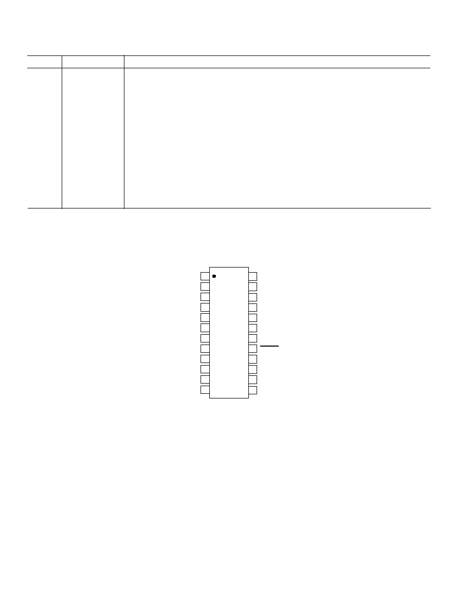
PIN CONFIGURATION
SOIC Package
TOP VIEW
(Not to Scale)
ADE7752
REFIn/Out
AGND
ICN
ICP
IBN
CF
DGND
VDD
REVP
IBP
IAN
IAP
VN
VCP
VBP
VAP
RESET
S0
F2
S1
F1
SCF
CLKIN
CLKOUT
2
3
4
5
6
7
8
9
10
11
12
1
24
23
22
21
20
19
18
17
16
15
14
13
REV. PrB 08/01
7
PRELIMINARY TECHNICAL DATA
ADE7752
Meter connections
In three phase service, two main power distribution services
exist: 3-phase 4-wire or 3-phase 3-wire. The additional wire
in the 3-phase 4-wire arrangement is the Neutral wire. The
voltage lines have a phase difference of ±120° (± 2
/3
radians) between each other - See Equation 5.
)
3
4
cos(
2
)
(
)
3
2
cos(
2
)
(
;
)
cos(
2
)
(
+
=
+
=
=
t
V
t
V
t
V
t
V
t
V
t
V
l
C
C
l
B
B
l
A
A
(5)
Where: V
A
, V
B
and V
C
represent the voltage RMS value of the
different phases
The current inputs are represented by Equations 6,
)
3
4
cos(
2
)
(
)
3
2
cos(
2
)
(
;
)
cos(
2
)
(
C
l
C
C
B
l
B
B
A
l
A
A
t
I
t
I
t
I
t
I
t
I
t
I
+
+
=
+
+
=
+
=
(6)
Where: I
A
, I
B
and I
C
represent the RMS value of the current
of each phase and
A
,
B
and
C
the phase difference of the
current and voltage channel of each phase.
The instantaneous powers can then be calculated as follows:
)
(
)
(
)
(
)
(
)
(
)
(
)
(
)
(
)
(
t
I
t
V
t
P
t
I
t
V
t
P
t
I
t
V
t
P
C
C
C
B
B
B
A
A
A
=
=
=
Then,
)
3
8
2
cos(
)
cos(
)
(
)
3
4
2
cos(
)
cos(
)
(
)
2
cos(
)
cos(
)
(
C
l
C
C
C
C
C
C
B
l
B
B
B
B
B
B
A
l
A
A
A
A
A
A
t
I
V
I
V
t
P
t
I
V
I
V
t
P
t
I
V
I
V
t
P
+
+
-
=
+
+
-
=
+
-
=
(7)
As can be seen from Equation 7, in the ADE7752 the real
power calculation per phase is made when current and voltage
inputs of the one phase are connected to the same channel (A,
B or C). Then, the summation of each individual real power
calculation gives the total Real Power information. P(t) =
P
A
(t) + P
B
(t) + P
C
(t)
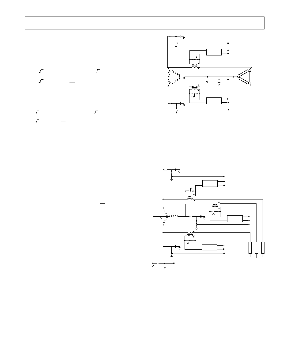
Figure 14 demonstrates the connections of the analog inputs
of the ADE7752 with the power lines in a 3-phase 3-wire
Delta service.
Source
CT
CT
Rb
Rb
IAP
IAN
Anti-aliasing
Filters
IBP
IBN
Anti-aliasing
Filters
Ra*
Rb*
VR*
Rf
Cf
Cf
VN
VAP
Ra*
Rb*
VR*
Cf
VBP
Load
Phase A
Phase B
Phase C
Figure 14 - 3-phase 3-wire meter connection with ADE7752
Note: Only 2 current inputs and 2 voltage inputs of the
ADE7752 are used in this case. The Real power calculated
by the ADE7752 does not depend on the selected channel.
Figure 15 demonstrates the connections of the analog inputs
of the ADE7752 with the power lines in a 3-phase 4-wire Wye
service.
Source
CT
CT
Rb
Rb
IAP
IAN
Anti-aliasing
Filters
ICP
ICN
Anti-aliasing
Filters
Ra*
Rb*
VR*
Rf
Cf
Cf
VN
VAP
Ra*
Rb*
VR*
Cf
VCP
Load
CT
Rb
IBP
IBN
Anti-aliasing
Filters
Ra*
Rb*
VR*
Cf
VBP
Phase A
Phase B
Phase C
Figure 15 - 3-phase 4-wire meter connection with ADE7752
REV. PrB 08/01
PRELIMINARY TECHNICAL DATA
ADE7752
8
TRANSFER FUNCTION
Frequency Outputs F1 and F2
The ADE7752 calculates the product of six voltage signals
(on Current channel and Voltage channel) and then low-pass
filters this product to extract real power information. This
real power information is then converted to a frequency. The
frequency information is output on F1 and F2 in the form of
active high pulses. The pulse rate at these outputs is relatively
low, e.g., 0.08 Hz maximum for AC signals with SCF = S0
= S1 = 1--see Table III. This means that the frequency at
these outputs is generated from real power information
accumulated over a relatively long period of time. The result
is an output frequency that is proportional to the average real
power. The averaging of the real power signal is implicit to
the digital-to-frequency conversion. The output frequency or
pulse rate is related to the input voltage signals by the
following equation.
(
)
2
5
1
2
.
109
REF
C
CN
B
BN
A
AN
V
F
I
V
I
V
I
V
Freq
-
×
×
+
×
+
×
×
=
where:
Freq
= Output frequency on F1 and F2 (Hz)
V
AN
, V
BN
and V
CN
= Differential rms voltage signal on Volt-
age channels (volts)
I
A
, I
B
and I
C
= Differential rms voltage signal on Current
channels (volts)
V
REF
=
The reference voltage (2.5 V ± 8%) (volts)
F
15
=
One of five possible frequencies selected by
using the logic inputs SCF, S0 and S1--see
Table II.
Table II. F
15
Frequency Selection
SCF
S1
S0
F
15
(Hz)
XTAL/CLKIN*
1
1
1
0.596
10 MHz/2
24
0
1
1
76.3
10 MHz/2
17
-
1
0
19.07
10 MHz/2
19
-
0
1
4.77
10 MHz/2
21
-
0
0
1.19
10 MHz/2
23
NOTE
*F
15
is a binary fraction of the master clock and therefore will vary if the specified
CLKIN frequency is altered.
Example 1
Thus if full-scale differential DC voltages of +125 mV and
125 mV are applied to VA, VB, VC, IA, IB and IC respec-
tively (125 mV is the maximum differential voltage that
can be connected to Current and Voltage channels), the
expected output frequency is calculated as follows:
F
15
=
0.596 Hz, SCF = S0 = S1 = 1
V
AN
= V
BN
= V
CN
= IA = IB = IC
= +125 mV dc = 0.125 V (rms of dc = dc)
V
REF
=
2.5 V (nominal reference value).
NOTE: If the on-chip reference is used, actual
output frequencies may vary from device to device
due to reference tolerance of ±8%.
Hz
Freq
488
.
0
5
.
2
596
.
0
125
.
0
125
.
0
2
.
109
3
2
=
×
×
×
×
=
Example 2
In this example, with AC voltages of ±500 mV peak ap-
plied to the Voltage channels and Current channels, the
expected output frequency is calculated as follows:
F
15
= 0.596 Hz, SCF = S0 = S1 = 1
V
AN
= V
BN
= V
CN
= IA = IB = IC
= 125 mV peak AC = 0.125/
2
volts rms
V
REF
= 2.5 V (nominal reference value).
NOTE: If the on-chip reference is used, actual
output frequencies may vary from device to device
due to reference tolerance of ±8%.
Hz
Freq
24
.
0
5
.
2
2
2
596
.
0
125
.
0
125
.
0
2
.
109
3
2
=
×
×
×
×
×
×
=
As can be seen from these two example calculations, the
maximum output frequency for AC inputs is always half of
that for DC input signals. The maximum frequency depends
also on the number of phases connected to the ADE7752. In
a 3-phase 3-wire delta service the maximum output frequency
is different from the maximum output frequency in a 3-phase
4-wire Wye service. The reason is that there are only 2 phases
connected to the analog inputs but also that in a delta service,
the Current channel input and Voltage channel input of the
same phase are not in phase in normal operation.
Example 3
In this example, the ADE7752 is connected to a 3-phase 3-
wire delta service as shown in Figure 14. The total real energy
calculation processed in the ADE7752 can be expressed as:
(
)
(
)
B
C
B
A
C
A
I
V
V
I
V
V
Energy
al
Total
×
-
+
×
-
=
Re
Where V
A
, V
B
and V
C
represent respectively the voltage on
phase A, B and C. I
A
and I
B
represent respectively the current
on phase A and B.
As the voltage and current inputs respect Equations 5 and 6,
the Total Real Energy (P) is:
REV. PrB 08/01
9
PRELIMINARY TECHNICAL DATA
ADE7752
( )
( )
+
+
-
+
+
+
-
=
-
×
-
+
-
×
-
=
3
2
cos
2
3
4
cos
2
3
2
cos
2
cos
2
3
4
cos
2
cos
2
)
(
)
(
)
(
)
(
t
I
t
V
t
V
t
I
t
V
t
V
P
IBN
IBP
VC
VB
IAN
IAP
VC
VA
P
l
B
l
C
l
B
l
A
l
C
l
A
For simplification, we assume that
A
=
B
=
C
= 0 and V
A
= V
B
=V
C
= V. The equation above becomes:
( )
(
)
+
+
+
+
=
3
2
cos
sin
3
sin
2
cos
3
2
sin
3
2
sin
2
t
t
I
V
t
t
I
V
P
l
l
B
l
l
A
(9)
P then becomes:
+
+
+
+
+
=
3
2
sin
3
sin
3
2
2
sin
3
2
sin
t
I
V
t
I
V
P
l
B
BN
l
A
AN
(10)
Where:
V
AN
= V . sin(2
/3) represents the RMS voltage between
VAP and VN pins of the ADE7752
V
BN
= V . sin (
/3) represents the RMS voltage between
VBP and VN pins of the ADE7752.
As the LPF on each channel eliminates the 2
l
component of
the equation, the Real power measured by the ADE7752 is:
2
3
2
3
+
=
B
BN
A
AN
I
V
I
V
P
Where:
V
AN
and V
BN
are the voltage RMS at the voltage inputs of
the ADE7752 after voltage sensing
I
A
and I
B
are the voltage RMS at the current input of the
ADE7752 after current sensing
If full scale AC voltage of ±125 mV peak are applied to the
Voltage channels and Current channels, the expected output
frequency is calculated as follows:
F
15
= 0.596 Hz, SCF = S0 = S1 = 1
VAN = VBN = IA = IB
= 125 mV peak AC = 0.125/
2
volts rms
VCN = IC = 0
V
REF
= 2.5 V (nominal reference value).
NOTE: If the on-chip reference is used, actual
output frequencies may vary from device to
device due to reference tolerance of ±8%.
14
.
0
2
3
5
.
2
2
2
596
.
0
125
.
0
125
.
0
2
.
109
2
2
=
×
×
×
×
×
×
×
=
Freq
Table III shows a complete listing of all maximum output
frequencies when using all three channels inputs.
Table III. Maximum Output Frequency on F1 and F2
Max Frequency
Max Frequency
SCF
S1
S0
for DC Inputs (Hz)
for AC Inputs (Hz)
1
1
1
0.48
0.24
0
1
1
62.52
31.26
-
1
0
15.6
7.8
-
0
1
3.9
1.95
-
0
0
0.96
0.48
Frequency Output CF
The pulse output CF (Calibration Frequency) is intended for
use during calibration. The output pulse rate on CF can be
up to 160 times the pulse rate on F1 and F2. The lower the
F
15
frequency selected, the higher the CF scaling. Table IV
shows how the two frequencies are related, depending on the
states of the logic inputs S0, S1 and SCF. Because of its
relatively high pulse rate, the frequency at this logic output
is proportional to the instantaneous real power. As is the case
with F1 and F2, the frequency is derived from the output of
the low-pass filter after multiplication. However, because the
output frequency is high, this real power information is
accumulated over a much shorter time. Hence less averaging
is carried out in the digital-to-frequency conversion. With
much less averaging of the real power signal, the CF output
is much more responsive to power fluctuations--see Signal
Processing Block in Figure 8.
Table IV. Maximum Output Frequency on CF
SCF
S1
S0
F
15
(Hz)
CF Max for AC Signals (Hz)
0
0
0
1.19
160 x F1, F2 = 78.12
1
0
0
1.19
8 x F1, F2 = 3.90
0
0
1
4.77
160 x F1, F2 = 312.51
1
0
1
4.77
16 x F1, F2 = 31.26
0
1
0
19.07
16 x F1, F2 = 130.56
1
1
0
19.07
8 x F1, F2 = 62.49
0
1
1
76.29
8 x F1, F2 = 250
1
1
1
0.596
16 x F1, F2 = 3.90 Hz
Frequency Outputs
Figure 1 shows a timing diagram for the various frequency
outputs. The outputs F1 and F2 are the low frequency
outputs that can be used to directly drive a stepper motor or
electromechanical impulse counter. The F1 and F2 outputs
provide two alternating high going pulses. The pulsewidth
(t
1
) is set at 275 ms and the time between the rising edges of
F1 and F2 (t
3
) is approximately half the period of F1 (t
2
). If
however the period of F1 and F2 falls below 550 ms (1.81 Hz)
the pulsewidth of F1 and F2 is set to half of their period. The
maximum output frequencies for F1 and F2 are shown in
Table III.
The high frequency CF output is intended to be used for
communications and calibration purposes. CF produces a
90 ms-wide active high pulse (t
4
) at a frequency proportional
to active power. The CF output frequencies are given in
Table IV. As in the case of F1 and F2, if the period of CF
(t
5
) falls below 180 ms, the CF pulsewidth is set to half the
period. For example, if the CF frequency is 20 Hz, the CF
pulsewidth is 25 ms.
REV. PrB 08/01
PRELIMINARY TECHNICAL DATA
ADE7752
1 0
NO LOAD THRESHOLD
The ADE7752 also includes a "no load threshold" and
"start-up current" feature that will eliminate any creep
effects in the meter. The ADE7752 is designed to issue a
minimum output frequency. Any load generating a frequency
lower than this minimum frequency will not cause a pulse to
be issued on F1, F2 or CF. The minimum output frequency
is given as 0.0007% of the full-scale output frequency for
each of the F
15
frequency selections--see Table II. For
example, an energy meter with a meter constant of 100 imp/
kWhr on F1, F2 using F
2
(4.77 Hz), the minimum output
frequency at F1 or F2 would be 0.0007% of 4.77 Hz or 33.3
x 10
6
Hz. This would be 533 x 10
6
Hz at CF (16 x F1 Hz).
In this example the no load threshold would be equivalent to
1.2 W of load or a start-up current of 5.5 mA at 220 V.
REVERSE POWER INFORMATION
The ADE7752 detects when the current and voltage channels
of any of the three phase inputs have a phase difference
greater than 90° i.e.
A
or
B
or
C
> 90°. This mechanism
can detect wrong connection of the meter or generation of
Active Energy.
The REVP pin output will go active high when negative
power is detected on any of the three phase inputs. If positive
Active Energy is detected on all the three phases, REVP pin
output is Low. The REVP pin output changes state at the
same time as a pulse is issued on CF. If several phases
measure negative power, the REVP pin output will stay low
until all the phases measure positive power.
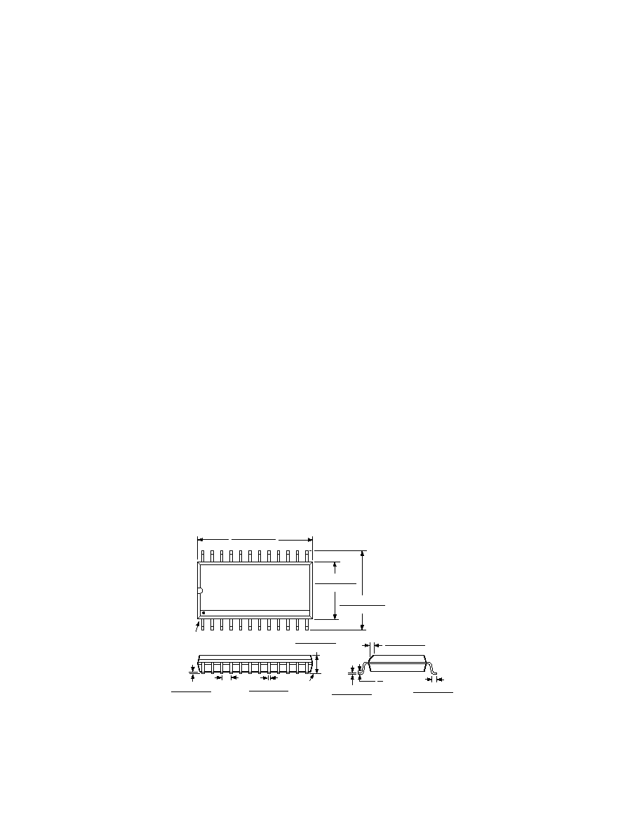
OUTLINE DIMENSIONS
Dimensions shown in inches and (mm).
0.0125 (0.32)
0.0091 (0.23)
8
0
0.0291 (0.74)
0.0098 (0.25)
45
0.0500 (1.27)
0.0157 (0.40)
SEATING
PLANE
0.0118 (0.30)
0.0040 (0.10)
0.0192 (0.49)
0.0138 (0.35)
0.1043 (2.65)
0.0926 (2.35)
0.0500
(1.27)
BSC
24
13
12
1
0.4193 (10.65)
0.3937 (10.00)
0.2992 (7.60)
0.2914 (7.40)
PIN 1
0.6141 (15.60)
0.5985 (15.20)
24-SOIC Outline Package
(AR-24)
N O T E
For a complete datasheet of the ADE7752, please contact us
on our website at:
http://forms.analog.com/Form_Pages/energymeter/
contact.asp
Document Outline
- Specifications
- Pinout
- Package Drawings
- Ordering Guide
- Features
- Absolute Maximum Ratings
- Functional Block Diagram
- Pin Function Description
- CAUTION
- TERMINOLOGY MEASUREMENT ERROR
- PHASE ERROR BETWEEN CHANNELS
- GAIN ERROR
- POWER SUPPLY REJECTION
- NO LOAD THRESHOLD NOTE
- REVERSE POWER INFORMATION
- DIAGRAMS
- Timing Diagram for Frequency Outputs
- phase 3-wire meter connection with ADE7752
- 3-phase 4-wire meter connection with ADE7752