Document Outline
- FEATURES
- ţ˙
- ţ˙
- ţ˙
- ţ˙
- ţ˙
- ţ˙
- ţ˙
- ţ˙
- ţ˙
- ţ˙
- ţ˙
Rail-to-Rail, Fast, Low Power, 2.5 V to 5.5 V,
Single-Supply TTL/CMOS Comparators
Preliminary Technical Data
ADCMP608/ACMP609
Rev. PrA
Information furnished by Analog Devices is believed to be accurate and reliable. However, no
responsibility is assumed by Analog Devices for its use, nor for any infringements of patents or other
rights of third parties that may result from its use. Specifications subject to change without notice. No
license is granted by implication or otherwise under any patent or patent rights of Analog Devices.
Trademarks and registered trademarks are the property of their respective owners.
One Technology Way, P.O. Box 9106, Norwood, MA 02062-9106, U.S.A.
Tel: 781.329.4700
www.analog.com
Fax: 781.461.3113
©2006 Analog Devices, Inc. All rights reserved.
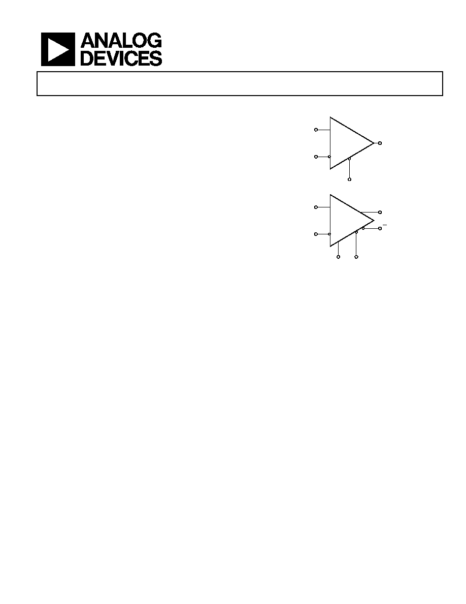
FUNCTIONAL BLOCK DIAGRAMS
FEATURES
NONINVERTING
INPUT
INVERTING
INPUT
Q OUTPUT
Q OUTPUT
ADCMP609
+
S
DN
LE/HYS
ADCMP608
NONINVERTING
INPUT
INVERTING
INPUT
Q OUTPUT
+
S
DN
05
91
8-
00
1
10 mV sensitivity rail to rail at V
CC
= 2.5 V
Input common-mode voltage from -0.2 V to V
CC
+ 0.2 V
Low glitch CMOS-/TTL-compatible output stage
30 ns propagation delay
1 mW at 2.5 V
Shutdown pin
Single-pin control for programmable hysteresis and latch
Power supply rejection >60 dB
-40C° to +125C° operation
APPLICATIONS
High speed instrumentation
Clock and data signal restoration
Logic level shifting or translation
High speed line receivers
Threshold detection
Peak and zero-crossing detectors
Figure 1.
High speed trigger circuitry
Pulse-width modulators
Current-/voltage-controlled oscillators
GENERAL DESCRIPTION
The ADCMP608 and ADCMP609 are fast comparators
fabricated on Analog Devices' proprietary XFCB2 process.
These comparators are exceptionally versatile and easy to use.
Features include an input range from V
EE
- 0.5 V to V
CC
+ 0.5 V,
low noise, TTL-/CMOS-compatible output drivers, and latch
inputs with adjustable hysteresis and/or shutdown inputs.
The TTL-/CMOS-compatible output stage is designed to drive
up to 15 pF with full rated timing specs and to degrade in a
graceful and linear fashion as additional capacitance is added.
The comparator input stage offers robust protection against
large input overdrive, and the outputs do not phase reverse
when the valid input signal range is exceeded. High speed latch
and programmable hysteresis features are also provided in a
unique single-pin control option.
The devices offer 30 ns propagation delays driving a 15 pF load
with 5 mV overdrive on 350/400 A typical supply current. A
flexible power supply scheme allows the devices to operate with
a single +2.5 V positive supply and a -0.5 V to +3.0 V input
signal range up to a +5.5 V positive supply with a -0.5 V to +6V
input signal range. Split input/output supplies, with no
sequencing restrictions on the ADCMP609, support a wide
input signal range while allowing independent output swing
control.
The ADCMP608 is available in a tiny 6-lead SC70 package with
single-ended output and a shutdown pin.
The ADCMP609, available in an 8-lead MSOP package, features
a shutdown pin, single pin latch, and hysteresis control.
+

ADCMP608/ADCMP609
Preliminary Technical Data
Rev. PrA | Page 2 of 16
TABLE OF CONTENTS
Features .............................................................................................. 1
Applications....................................................................................... 1
Functional Block Diagrams............................................................. 1
General Description ......................................................................... 1
Revision History ............................................................................... 2
Specifications..................................................................................... 3
Electrical Characteristics............................................................. 3
Absolute Maximum Ratings............................................................ 5
Thermal Resistance ...................................................................... 5
ESD Caution.................................................................................. 5
Pin Configuration and Function Descriptions............................. 6
Typical Performance Characteristics ............................................. 7
Application Information...................................................................9
Power/Ground Layout and Bypassing........................................9
TTL-/CMOS-Compatible Output Stage.........................................9
Using/Disabling the Latch Feature..............................................9
Optimizing Performance..............................................................9
Comparator Propagation Delay Dispersion ........................... 10
Comparator Hysteresis .............................................................. 10
Crossover Bias Point .................................................................. 11
Minimum Input Slew Rate Requirement ................................ 11
Typical Application Circuits ......................................................... 12
Timing Information ....................................................................... 13
REVISION HISTORY
2/06--Revision PrA: Preliminary Version
Preliminary Technical Data
ADCMP608/ADCMP609
Rev. PrA | Page 3 of 16
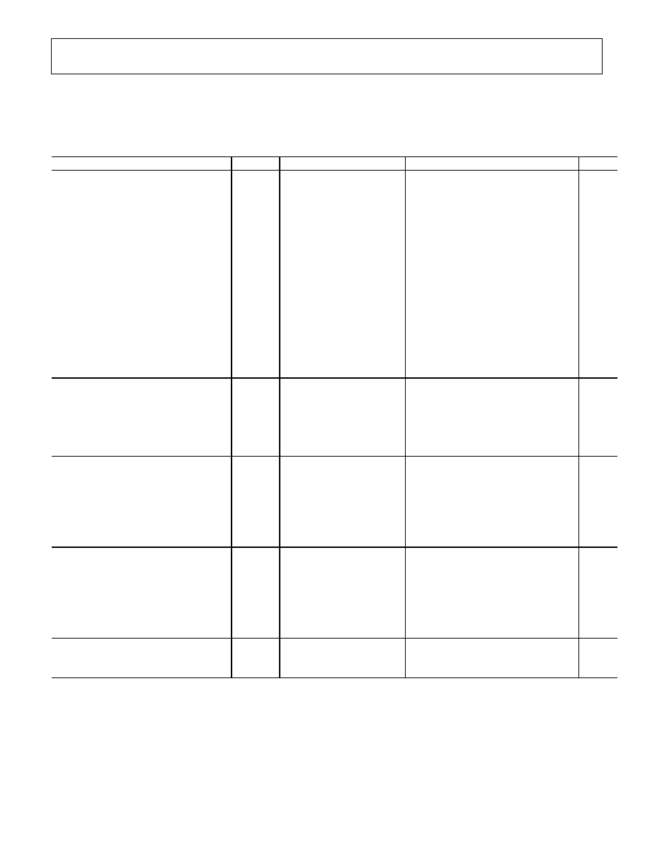
SPECIFICATIONS
ELECTRICAL CHARACTERISTICS
V
CCI
= V
CCO
= 3.3 V, T
A
= 25°C, unless otherwise noted.
Table 1.
Parameter Symbol
Conditions
Min
Typ
Max
Unit
DC
INPUT
CHARACTERISTICS
Voltage Range
V
P
, V
N
V
CC
= 2.5 V to 5.5 V
-0.5
V
CC
+ 0.5 V
V
Common-Mode Range
V
CC
= 2.5 V to 5.5 V
-0.2
V
CC
+ 0.2 V
V
Differential Voltage
V
CC
= 2.5 V to 5.5 V
V
CC
V
Offset Voltage
V
OS
-5.0
+5.0 mV
Bias Current
I
P
, I
N
-2.0 ±1 +2.0 A
Offset
Current
-0.5
+0.5 A
Capacitance C
P
, C
N
TBD
pF
Resistance, Differential Mode
0.1 V to V
CC
150
k
Resistance, Common Mode
-0.5 V to V
CC
+ 0.5 V
100
k
Active Gain
A
V
80
dB
V
CCI
= 2.5 V, V
CCO
= 2.5 V,
V
CM
= -0.2 V to 2.7 V
50
dB
Common-Mode Rejection
CMRR
V
CCI
= 5.5 V, V
CCO
= 5.5 V,
V
CM
= -0.2 V to 5.7 V
60
dB
Hysteresis
R
HYS
=
0.1
mV
LATCH
ENABLE
PIN
CHARACTERISTICS
ADCMP609
only
V
IH
Hysteresis is shut off
2.0
V
CCO
+ 0.2
V
V
IL
Latch mode guaranteed
-0.2
0.4
0.8
V
L
IH
V
IH
= V
CCO
+ 0.2 V
0.1
mA
I
OL
V
IL
= 0.4 V
-0.1
mA
HYSTERESIS
MODE
AND
TIMING
Hysteresis Mode Bias Voltage
Current sink 0 A
1.08
1.25
1.35
V
Minimum Resistor Value
Hysteresis = 60 mV
60
k
Latch Setup Time
t
S
V
OD
= 100 mV
15
ns
Latch Hold Time
t
H
V
OD
= 100 mV
20
ns
Latch to Output Delay
t
PLOH,
t
PLOL
V
OD
= 100 mV
20
ns
Latch Minimum Pulse Width
t
PL
V
OD
= 100 mV
20
ns
SHUTDOWN
PIN
CHARACTERISTICS
V
IH
Comparator is operating
2.0
V
CC
V
V
IL
Shutdown
guaranteed
-0.2
0.4 0.6 V
I
IH
V
IH
= V
CC
0.05
mA
I
OL
V
IL
= 0 V
-0.05
mA
Sleep Time
t
SD
I
CC
< 100 A
0.6
ns
Wake-Up Time
t
H
V
OD
= 10 mV, output valid
3
ns
DC OUTPUT CHARACTERISTICS
V
CCO
=
2.5
V
to
6
V
Output Voltage High Level
V
OH
I
OH
= 1.6 mA V
CCO
= 2.5 V
V
CC
- 0.4
V
Output Voltage Low Level
V
OL
I
OL
= 1.6 mA V
CCO
= 2.5 V
0.4
V

ADCMP608/ADCMP609
Preliminary Technical Data
Rev. PrA | Page 4 of 16
Parameter Symbol
Conditions
Min
Typ
Max
Unit
AC PERFORMANCE
V
CCI
= V
CCO
= 2.5 V to 5.5 V
Propagation Delay, C
L
= 15 pF
t
PD
V
CCO
= 5.5 V to 2.5 V,
V
OD
= 10 mV
30
ns
V
CCO
= 2.5 V/5.5 V,
V
OD
= 200 mV
25/30
ns
Propagation Delay Skew--Rising to
Falling Transition
V
OD
= 10 mV
2
ns
Overdrive Dispersion
10 mV < V
OD
< 500 mV
4
ns
Slew Rate Dispersion
Small Signal
10 V/s to 0.1 V/ns
200 mV p-p single ended
1
ns
10% - 90% Duty Cycle Dispersion
V
OD
1.25 V, 50 V/s,
V
CM
= 1.25 V
1
ns
Common-Mode Dispersion
V
CM
= 0 V to V
CC
200 m p-p single ended
0.5
ns
Toggle Rate
>50% output swing
C
L
= 15 pF V
CCI
= 5 V
TBD
Mbps
RMS Random Jitter
RJ
V
OD
= 200 mV, 5 V/ns
TBD
ns
Minimum Pulse Width
PW
MIN
t
PD
/PW < 500 ps
35
ns
Rise Time
t
R
10% to 90% C
LOAD
= 15 pF,
V
CCI
= 2.5 V to 5 V
25 to 40
ns
Fall Time
t
F
10% to 90% C
LOAD
= 15 pF,
V
CCI
= 2.5 V to 5 V
25 to 40
ns
POWER
SUPPLY
Input Supply Voltage Range
V
CCI
2.5
5.5 V
Output Supply Voltage Range
V
CCO
2.5
5.5 V
Positive Supply Differential
(ADCMP609)
V
CCI
- V
CCO
Operating
-3
+3 V
Positive Supply Differential
(ADCMP609)
V
CCI
- V
CCO
Nonoperating
-5.5
+5.5 V
Positive Supply Current
I
VCC
V
CC
= 2.5 V
400
A
Positive Supply Current
I
VCC
V
CC
= 5.5 V
500
A
Input Section Supply Current
(ADCMP609)
I
VCCi
V
CCI
= 2.5 V
270
mA
Output Stage Supply Current
(ADCMP609)
I
VCCO
V
CCO
=
2.5
V
130
mA
Power Dissipation
P
D
V
CC
= 2.5 V
1
mW
Shutdown Current
I
SD
V
CC
=2.5 V to 5.5 V
50
A
Power Supply Rejection
PSRR
V
CCI
= 2.5 V to 5 V
>50 dB
dB

Preliminary Technical Data
ADCMP608/ADCMP609
Rev. PrA | Page 5 of 16
ABSOLUTE MAXIMUM RATINGS
Table 2.
Parameter Rating
Stress above those listed under Absolute Maximum Ratings may
cause permanent damage to the device. This is a stress rating
only and functional operation of the device at these or any other
conditions above those indicated in the operational sections of
this specification is not implied. Exposure to absolute
maximum rating conditions for extended periods may affect
device reliability.
Supply Voltages
Input Supply Voltage (V
CCI
to GND)
-0.5 V to +6.0 V
-0.5 V to +6.0 V
Output Supply Voltage
(V
CCO
to GND)
-6.0 V to +6.0 V
Positive Supply Differential
(V
CCI
- V
CCO
)
Input Voltages
THERMAL RESISTANCE
Input Voltage
-0.5 V to V
CCI
+ 0.5 V
JA
is specified for the worst-case conditions, that is, a device
soldered in a circuit board for surface-mount packages.
Differential Input Voltage
±(V
CCI
+ 0.5 V)
Maximum Input/Output Current
±50mA
Table 3. Thermal Resistance
Shutdown Control Pin
Package Type
JA
Unit
1
Applied Voltage (HYS to GND)
-0.5 V to Vcco + 0.5 V
ADCMP608 SC70 6-lead
426
°C/W
Maximum Input/Output Current
±50 mA
ADCMP609 MSOP 8-lead
130
°C/W
Latch/Hysteresis Control Pin
Applied Voltage (HYS to GND)
-0.5 V to V
CCO
+ 0.5 V
1
Measurement in still air.
Maximum Input/Output Current
±50 mA
Output Current
±50 mA
Temperature
Operating Temperature, Ambient
-40°C to +125°C
Operating Temperature, Junction
150°C
Storage Temperature Range
-65°C to +150°C
ESD CAUTION
ESD (electrostatic discharge) sensitive device. Electrostatic charges as high as 4000 V readily accumulate on
the human body and test equipment and can discharge without detection. Although this product features
proprietary ESD protection circuitry, permanent damage may occur on devices subjected to high energy
electrostatic discharges. Therefore, proper ESD precautions are recommended to avoid performance
degradation or loss of functionality.

ADCMP608/ADCMP609
Preliminary Technical Data
Rev. PrA | Page 6 of 16
PIN CONFIGURATION AND FUNCTION DESCRIPTIONS
ADCMP608
TOP VIEW
(Not to Scale)
Q
1
V
CC
6
V
EE
2
S
DN
5
V
P
3
V
N
4
05
91
8-
0
02
ADCMP609
TOP VIEW
(Not to Scale)
V
CC
1
Q
8
V
P
2
Q
7
V
N
3
V
EE
6
S
DN
4
LE/HYS
5
05
91
8-
0
03
Figure 2. ADCMP608 Pin Configuration
Figure 3. ADCMP609 Pin Configuration
Table 4. ADCMP608 Pin Function Descriptions
Pin No.
Mnemonic
Description
1 Q
Noninverting Output. Q is at logic high if the analog voltage at the noninverting input, V
P
, is greater than the
analog voltage at the inverting input, V
N
.
2 V
EE
Negative
Supply
Voltage.
3 V
P
Noninverting Analog Input.
4 V
n
Inverting Analog Input.
5 S
DN
Shutdown. Drive this pin low to shutdown the device.
6 V
CC
V
CC
Supply.
Table 5. ADCMP609 Pin Function Descriptions
Pin No.
Mnemonic
Description
1 V
CCI
/V
CCO
Vcc
Supply.
2 V
P
Noninverting Analog Input.
3 V
n
Inverting Analog Input.
4 S
DN
Shutdown. Drive this pin low to shutdown the device.
5
LE/HYS
Latch/Hysteresis Control. Bias with resistor or current source for hysteresis; drive TTL low to latch.
6 V
EE
Negative
Supply
Voltage.
7 Q Noninverting Output. Q is at logic low if the analog voltage at the noninverting input, V
P
, is greater than the
analog voltage at the inverting input, V
N
, provided the comparator is in compare mode.
8
Q
Inverting Output. Q is at logic high if the analog voltage at the noninverting input V
P
is greater than the analog
voltage at the inverting input, V
N
, provided the comparator is in compare mode.

Preliminary Technical Data
ADCMP608/ADCMP609
Rev. PrA | Page 7 of 16
TYPICAL PERFORMANCE CHARACTERISTICS
V
CCI
= V
CCO
= 3.3 V, T
A
= 25°C, unless otherwise noted.
Figure 4. Propagation Delay vs. Input Overdrive
Figure 7. Hysteresis vs. Vcc
Figure 5. Propagation Delay vs. Input Common Mode
Figure 8. Hysteresis vs. R
HYS
Control Resistor
Figure 9. Input Bias Current vs. Input Common Mode
Figure 6. Propagation Delay vs. Temperature
ADCMP608/ADCMP609
Preliminary Technical Data
Rev. PrA | Page 8 of 16
Figure 10. Input Bias Current vs. Temperature
Figure 12 Latch/Hysteresis Control Pin I/V Characteristic.
Figure 11. Input Offset Voltage vs. Temperature

Preliminary Technical Data
ADCMP608/ADCMP609
Rev. PrA | Page 9 of 16
APPLICATION INFORMATION
OUTPUT
Q2
Q1
+IN
IN
OUTPUT STAGE
V
LOGIC
GAIN STAGE
A2
A1
A
V
059
18
-
01
2
POWER/GROUND LAYOUT AND BYPASSING
The ADCMP608 and ADCMP609 comparators are high speed
devices. Despite the low noise output stage, it is essential to use
proper high speed design techniques to achieve the specified
performance. Because comparators are uncompensated
amplifiers, feedback in any phase relationship is likely to cause
oscillations or undesired hysteresis. Of critical importance is the
use of low impedance supply planes, particularly the output
supply plane (V
CCO
) and the ground plane (GND). Individual
supply planes are recommended as part of a multilayer board.
Providing the lowest inductance return path for switching
currents ensures the best possible performance in the target
application.
Figure 13. Simplified Schematic Diagram
of TTL/CMOS-COMPATIBLE Output Stage
It is also important to adequately bypass the input and output
supplies. A 0.1 F bypass capacitor should be placed as close as
possible to each V
CC
supply pin. The capacitor should be
connected to the GND plane with redundant vias placed to
provide a physically short return path for output currents
flowing back from ground to the V
CC
pin. High frequency
bypass capacitors should be carefully selected for minimum
inductance and ESR. Parasitic layout inductance should also be
strictly controlled to maximize the effectiveness of the bypass at
high frequencies.
USING/DISABLING THE LATCH FEATURE
The latch input of the ADCMP609 is designed for maximum
versatility. It can safely be left floating or pulled to TTL high for
normal comparator operation with no hysteresis, or it can be
driven low by any standard TTL/CMOS device as a high speed
latch.
In addition, the pin can be operated as a hysteresis control pin
with a bias voltage of 1.25 V nominal and an input resistance of
approximately 7000 . This allows the comparator hysteresis to
be easily and accurately controlled by either a resistor or an
inexpensive CMOS DAC.
TTL-/CMOS-COMPATIBLE OUTPUT STAGE
Specified propagation delay performance can be achieved only
by keeping the capacitive load at or below the specified mini-
mums. The outputs of the ADCMP608 and ADCMP609 are
designed to directly drive one Schottky TTL or three low power
Schottky TTL loads or equivalent. For large fan outs, buses, or
transmission lines, an appropriate buffer should be used to
maintain the excellent speed and stability of the part.
Hysteresis control and latch mode can be used together if an
open drain, a collector, or a three-state driver is connected in
parallel to the hysteresis control resistor or current source.
Due to the programmable hysteresis feature,the logic threshold
of the latch pin is approximately 1.1 V regardless of V
CC
.
With the rated 15 pF load capacitance applied, even at 2.5 V
V
CC
, more than half of the total device propagation delay is
output stage slew time. Because of this, the total prop delay will
decrease as V
CCO
decreases and instability in the power supply
may show up as excess delay dispersion.
OPTIMIZING PERFORMANCE
As with any high speed comparator, proper design and layout
techniques are essential for obtaining the specified
performance. Stray capacitance, inductance, common power
and ground impedances, or other layout issues can severely limit
performance and often cause oscillation. The source impedance
should be minimized as much as is practicable. High source
impedance, in combination with the parasitic input capacitance
of the comparator, will cause an undesirable degradation in
bandwidth at the input, thus degrading the overall response.
Higher impedances encourage undesired coupling.
This delay is measured to the 50% point for whatever supply is
in use, so the fastest times will be observed with the V
CC
supply
at 2.5 V, and larger values will be observed when driving loads,
that switch at other levels. Overdrive and input slew rate
dispersions are not significantly affected by output loading and
V
CC
variations.
The TTL/CMOS-compatible output stage is shown in the
simplified schematic diagram of Figure 12. Because of its
inherent symmetry and generally good behavior, this output
stage is readily adaptable for driving various filters and other
unusual loads.
ADCMP608/ADCMP609
Preliminary Technical Data
Rev. PrA | Page 10 of 16
COMPARATOR PROPAGATION
DELAY DISPERSION
COMPARATOR HYSTERESIS
The addition of hysteresis to a comparator is often desirable in a
noisy environment, or when the differential input amplitudes
are relatively small or slow moving. The transfer function for a
comparator with hysteresis is shown in
The ADCMP608 and ADCMP609 comparator is designed to
reduce propagation delay dispersion over a wide input overdrive
range of 5 mV to V
CCI
- 1 V. Propagation delay dispersion is the
variation in propagation delay that results from a change in the
degree of overdrive or slew rate (how far or how fast the input
signal exceeds the switching threshold).
Figure 16. As the input
voltage approaches the threshold (0.0 V, in this example) from
below the threshold region in a positive direction, the
comparator switches from a low to a high when the input crosses
+V
H
/2. The new switching threshold becomes -V
H
/2. The
comparator remains in the high state until the threshold -V
H
/2
is crossed from below the threshold region in a negative
direction. In this manner, noise or feedback output signals
centered on 0.0 V input cannot cause the comparator to switch
states unless it exceeds the region bounded by ±V
H
/2.
Propagation delay dispersion is a specification that becomes
important in high speed, time-critical applications, such as data
communication, automatic test and measurement, and instru-
mentation. It is also important in event-driven applications,
such as pulse spectroscopy, nuclear instrumentation, and
medical imaging. Dispersion is defined as the variation in
propagation delay as the input overdrive conditions are changed
(see
OUTPUT
INPUT
0
V
OL
V
OH
+V
H
2
V
H
2
059
18
-
01
5
Figure 14 and Figure 15).
ADCMP608 and ADCMP609 dispersion is typically <5 ns as
the overdrive varies from 5 mV to 500 mV, and the input slew
rate varies from 2 V/ns to 10 V/ns. This specification applies to
both positive and negative signals because the device has very
closely matched delays for both positive-going and negative-
going inputs, and very low output skews. Remember to add the
actual device offset to the overdrive for repeatable dispersion
measurements.
Q/Q OUTPUT
INPUT VOLTAGE
500mV OVERDRIVE
10mV OVERDRIVE
DISPERSION
V
N
± V
OS
05
91
8
-
01
3
Figure 16. Comparator Hysteresis Transfer Function
The customary technique for introducing hysteresis into a
comparator uses positive feedback from the output back to the
input. One limitation of this approach is that the amount of
hysteresis varies with the output logic levels, resulting in
hysteresis that is not symmetric about the threshold. The
external feedback network can also introduce significant
parasitics that reduce high speed performance, and can even
induce oscillation in some cases.
Figure 14. Propagation Delay--Overdrive Dispersion
The ADCMP609 comparator offers a programmable hysteresis
feature that significantly improves accuracy and stability.
Connecting an external pull-down resistor or a current source
from the LE/HYS pin to GND, varies the amount of hysteresis
in a predictable and stable manner. Leaving the LE/HYS pin
disconnected or driving it high removes the hysteresis. The
maximum hysteresis that can be applied using this pin is
approximately 160 mV.
Q/Q OUTPUT
INPUT VOLTAGE
10V/ns
1V/ns
DISPERSION
V
N
± V
OS
05
91
8-
01
4
Figure 17 illustrates the amount of
hysteresis applied as a function of external resistor value.
Figure TBD illustrates hysteresis as a function of current.
Figure 15. Propagation Delay--Slew Rate Dispersion
Preliminary Technical Data
ADCMP608/ADCMP609
Rev. PrA | Page 11 of 16
The hysteresis control pin appears as a 1.25 V bias voltage seen
through a series resistance of 7k ± 20% throughout the
hysterisis control range. The advantages of applying hysteresis
in this manner are improved accuracy, improved stability,
reduced component count, and maximum versatility. An
external bypass capacitor is not recommended on the HYS pin
because it would likely degrade the jitter performance of the
device and impair the latch function. As described in
CROSSOVER BIAS POINT
Rail-to-rail inputs of this type, in both op amps and compara-
tors have a dual front-end design. Certain devices are active
near the V
CC
rail and others are active near the V
EE
rail. At some
predetermined point in the common-mode range, a crossover
occurs. At this point, normally V
CC
/2, the direction of the bias
current reverses and there are changes in measured offset
voltages and currents.
Using/Disabling the Latch Feature, hysteresis control need not
compromise the latch function.
With V
CC
less than 4 V, this crossover is at the expected V
CC
/2,
but with V
CC
greater than 4 V, the crossover point instead
follows V
CC
1:1, bringing it to approximately 3 V with V
CC
at
5 V. This means that the comparator input characteristics will
more closely resemble the inputs of non rail-to rail ground
sensing comparators such as the AD8611.
MINIMUM INPUT SLEW RATE REQUIREMENT
(Remove if device is stable.)
As with most high speed comparators, without hysteresis a
minimum slew rate must be met to ensure that the device does
not oscillate as the input signal crosses the threshold. This
oscillation is due to the high gain bandwidth of the comparator
in combination with feedback parasitics inherent in the package
and PC board. A minimum slew rate of TBD. V/s ensures
clean output transitions from the ADCMP608/ADCMP609
comparators without hysteresis. In many applications,
chattering is not harmful.
Figure 17. Hysteresis vs. R
HYS
Control Resistor
ADCMP608/ADCMP609
Preliminary Technical Data
Rev. PrA | Page 12 of 16
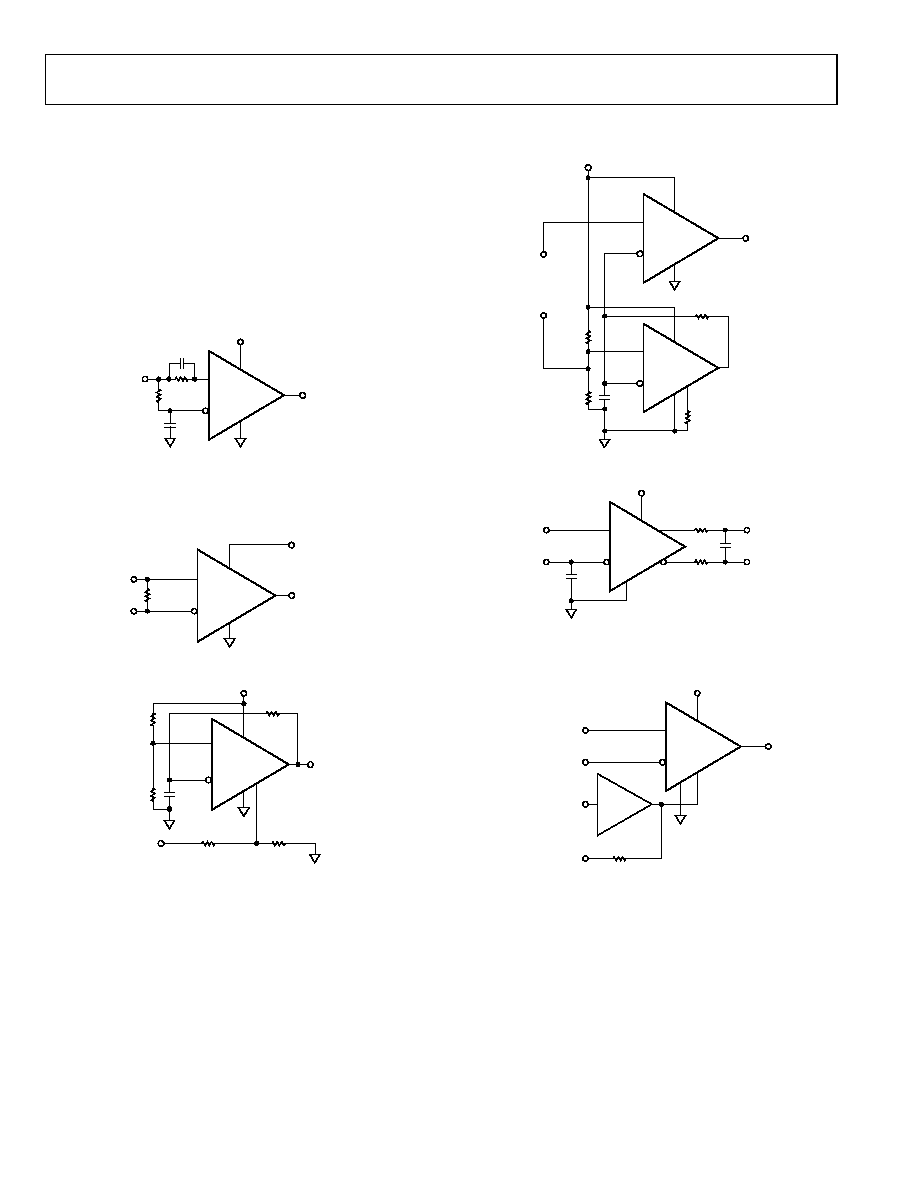
TYPICAL APPLICATION CIRCUITS
CMOS
PWM
OUTPUT
ADCMP608
2.5V
INPUT
1.25V
REF
INPUT
1.25V
±50mV
LE/HYS
ADCMP609
220pF
10k
10k
100k
10k
0
59
18
-
02
0
ADCMP608
OUTPUT
0.1µF
2.5V TO 5V
0.1µF
2k
2k
INPUT
05
91
8-
0
17
Figure 18. Self-Biased 50% Slicer
Figure 21. Oscillator and Pulse Width Modulator
ADCMP609
OUTPUT
+
5V
0.1µF
10k
10k
INPUT
V
REF
0.02µF
LE/HYS
0
59
18-
021
ADCMP608
CMOS
V
DD
2.5V TO 5V
100
LVDS
OUTPUT
05
91
8-
0
18
Figure 19. LVDS to CMOS Receiver
Figure 22. Duty Cycle to Differential Voltage
LE/HYS
ADCMP609
5V
150k
150k
CONTROL
VOLTAGE
0V TO 2.5V
OUTPUT
39k
39k
470pF
20k
05
91
8-
0
19
ADCMP609
2.5V TO 5V
10k
LE/HYS
DIGITAL
INPUT
HYSTERESIS
CURRENT
74AHC
1G07
05
91
8-
0
22
Figure 23. DAC Hysteresis Adjustment with Latch
Figure 20. Voltage Controlled Oscillator
Preliminary Technical Data
ADCMP608/ADCMP609
Rev. PrA | Page 13 of 16
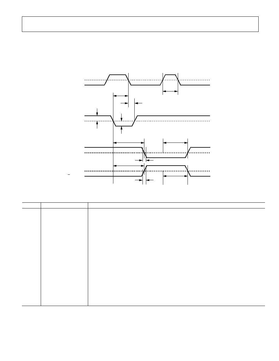
TIMING INFORMATION
Figure 24 illustrates the ADCMP608/ADCMP609 latch timing relationships. Table 6 provides definitions of the terms found in the figure.
1.1V
50%
V
N
± V
OS
50%
DIFFERENTIAL
INPUT VOLTAGE
LATCH ENABLE
Q OUTPUT
Q OUTPUT
t
H
t
PDL
t
PLOH
t
F
V
IN
V
OD
t
S
t
PL
t
PDH
t
PLOL
t
R
05
91
8-
0
23
Figure 24. System Timing Diagram
Table 6. Timing Descriptions
Symbol Timing
Description
t
PDH
Input to output high
delay
Propagation delay measured from the time the input signal crosses the reference (± the input offset
voltage) to the 50% point of an output low-to-high transition.
t
PDL
Input to output low
delay
Propagation delay measured from the time the input signal crosses the reference (± the input offset
voltage) to the 50% point of an output high-to-low transition.
t
PLOH
Latch enable to output
high delay
Propagation delay measured from the 50% point of the latch enable signal low-to-high transition to
the 50% point of an output low-to-high transition.
t
PLOL
Latch enable to output
low delay
Propagation delay measured from the 50% point of the latch enable signal low-to-high transition to
the 50% point of an output high-to-low transition.
t
H
Minimum hold time
Minimum time after the negative transition of the latch enable signal that the input signal must
remain unchanged to be acquired and held at the outputs.
t
PL
Minimum latch enable
pulse width
Minimum time that the latch enable signal must be high to acquire an input signal change.
t
S
Minimum setup time
Minimum time before the negative transition of the latch enable signal occurs that an input signal
change must be present to be acquired and held at the outputs.
t
R
Output rise time
Amount of time required to transition from a low to a high output as measured at the 20% and 80%
points.
t
F
Output fall time
Amount of time required to transition from a high to a low output as measured at the 20% and 80%
points.
V
OD
Voltage overdrive
Difference between the input voltages V
A
and V
B
.

ADCMP608/ACMP609
Preliminary Technical Data
Rev. PrA | Page 14 of 16
NOTES

Preliminary Technical Data
ADCMP608/ADCMP609
Rev. PrA | Page 15 of 16
NOTES

ADCMP608/ACMP609
Preliminary Technical Data
Rev. PrA | Page 16 of 16
NOTES
©2006 Analog Devices, Inc. All rights reserved. Trademarks and
registered trademarks are the property of their respective owners.
PR05918-0-2/06(PrA)