Document Outline
- ţ˙
- ţ˙
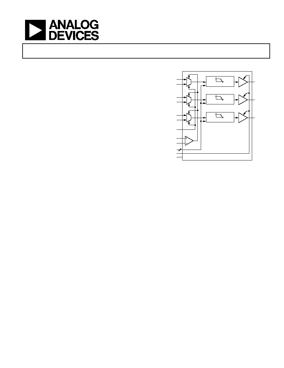
- FUNCTIONAL BLOCK DIAGRAM
- ţ˙
- ţ˙
- ţ˙
- ţ˙
- ţ˙
- ţ˙
- ţ˙
- ţ˙
- ţ˙
- ţ˙
- ţ˙
- ţ˙
- ţ˙
- ţ˙
- ţ˙
- INPUT AND OUTPUT COUPLING
- ţ˙
- ţ˙
Integrated Triple Video Filter and Buffer with Selectable
Cutoff Frequencies and Multiplexed Inputs for RGB, HD/SD
ADA4411-3
Rev. 0
Information furnished by Analog Devices is believed to be accurate and reliable. However, no
responsibility is assumed by Analog Devices for its use, nor for any infringements of patents or other
rights of third parties that may result from its use. Specifications subject to change without notice. No
license is granted by implication or otherwise under any patent or patent rights of Analog Devices.
Trademarks and registered trademarks are the property of their respective owners.
One Technology Way, P.O. Box 9106, Norwood, MA 02062-9106, U.S.A.
Tel: 781.329.4700
www.analog.com
Fax: 781.461.3113
© 2005 Analog Devices, Inc. All rights reserved.
FEATURES
FUNCTIONAL BLOCK DIAGRAM
Sixth-order adjustable video filters
0552
7-
001
CUTOFF SELECT
INPUT SELECT
DC
OFFSET
Y1/G1 IN
Y2/G2 IN
Pb1/B1 IN
Pb2/B2 IN
Pr1/R1 IN
Pr2/R2 IN
LEVEL2
LEVEL1
GAIN SELECT
2
Y/G OUT
Pb/B OUT
Pr/R OUT
DISABLE
36MHz, 18MHz, 9MHz
×2
×4
36MHz, 18MHz, 9MHz
×2
×4
36MHz, 18MHz, 9MHz
×2
×4
ADA4411-3
36 MHz, 18 MHz, and 9 MHz
Many video standards supported: RGB, YPbPr, YUV, SD, Y/C
Ideal for 720p and 1080i resolutions
-1 dB bandwidth of 30.5 MHz for HD
Low quiescent power
Only 265 mW for 3 channels on 5 V supply
Disable feature cuts supply current to 15 A
2:1 mux on all inputs
Variable gain: ×2 or ×4
DC output offset adjust: ±0.5 V, input referred
Excellent video specifications
Wide supply range: +4.5 V to ±5 V
Rail-to-rail output
Output can swing 4.5 V p-p on single 5 V supply
Small packaging: 24-lead QSOP
Figure 1.
APPLICATIONS
Set-top boxes
Personal video recorders
DVD players and recorders
HDTVs
Projectors
GENERAL DESCRIPTION
The ADA4411-3 is a comprehensive filtering solution designed
to give designers the flexibility to easily filter and drive various
video signals, including high definition video. Cutoff frequen-
cies of the sixth-order video filters range from 9 MHz to
36 MHz and can be selected by two logic pins to obtain four
filter combinations that are tuned for RGB, high definition, and
standard definition video signals. The ADA4411-3 has a rail-
to-rail output that can swing 4.5 V p-p on a single 5 V supply.
The ADA4411-3 can operate on a single +5 V supply as well as
on ±5 V supplies. Single-supply operation is ideal in
applications where power consumption is critical. The disable
feature allows for further power conservation by reducing the
supply current to typically 15 A when a particular device is not
in use.
Dual-supply operation is best for applications where the
negative-going video signal excursions must swing at or
below ground while maintaining excellent video performance.
The output buffers have the ability to drive two 75 doubly
terminated cables that are either dc-coupled or ac-coupled.
The ADA4411-3 offers gain and voltage offset adjustments.
With a single logic pin, the throughput filter gain can be
selected to be ×2 or ×4. Output voltage offset is continuously
adjustable over an input-referred range of ±500 mV by applying
a differential voltage to an independent offset control input.
The ADA4411-3 is available in the 24-lead, wide body
QSOP and is rated for operation over the extended
industrial temperature range of -40°C to +85°C.
The ADA4411-3 offers 2:1 multiplexers on all of its video
inputs, which are useful in applications where filtering is
required for multiple sources of video signals.

ADA4411-3
Rev. 0 | Page 2 of 16
TABLE OF CONTENTS
Features .............................................................................................. 1
Applications....................................................................................... 1
Functional Block Diagram .............................................................. 1
General Description ......................................................................... 1
Revision History ............................................................................... 2
Specifications..................................................................................... 3
Absolute Maximum Ratings............................................................ 5
Thermal Resistance ...................................................................... 5
ESD Caution.................................................................................. 5
Pin Configuration And Function Descriptions............................ 6
Typical Performance Characteristics ............................................. 7
Theory of Operation ...................................................................... 10
Applications..................................................................................... 11
Overview ..................................................................................... 11
Multiplexer Select Inputs........................................................... 11
Throughput Gain........................................................................ 11
Disable ......................................................................................... 11
Cutoff Frequency Selection....................................................... 11
Output DC Offset Control ........................................................ 11
Input and Output Coupling ...................................................... 12
Printed Circuit Board Layout ................................................... 13
Video Encoder Reconstruction Filter...................................... 13
Outline Dimensions ....................................................................... 15
Ordering Guide .......................................................................... 15
REVISION HISTORY
7/05--Revision 0: Initial Version

ADA4411-3
Rev. 0 | Page 3 of 16
SPECIFICATIONS
V
S
= 5 V, @ T
A
= 25°C, V
O
= 1.4 V p-p, G = ×2, R
L
= 150 , unless otherwise noted.
Table 1.
Parameter Test
Conditions/Comments
Min
Typ
Max
Unit
OVERALL
PERFORMANCE
Offset Error
Input referred, all channels
12
30
mV
Offset Adjust Range
Input referred
±500
mV
Input Voltage Range, All Inputs
V
S-
- 0.1
V
S+
- 2.0
V
Output Voltage Swing, All Outputs
Positive swing
V
S+
- 0.33
V
S+
- 0.22
V
Negative
swing
V
S-
+ 0.10
V
S-
+ 0.13
V
Linear Output Current per Channel
30
mA
Integrated Voltage Noise, Referred to Input
All channels
0.52
mV rms
Filter Input Bias Current
All channels
6.6
A
Total Harmonic Distortion at 1 MHz
F
C
= 36 MHz, F
C
= 18 MHz/F
C
= 9 MHz
0.01/0.04
%
Gain Error Magnitude
G = ×2/G = ×4
0.13/0.15
0.38/0.40
dB
FILTER DYNAMIC PERFORMANCE
-1 dB Bandwidth
Cutoff frequency select = 36 MHz
26.5
30.5
MHz
Cutoff frequency select = 18 MHz
13.5
15.5
MHz
Cutoff frequency select = 9 MHz
6.5
7.8
MHz
-3 dB Bandwidth
Cutoff frequency select = 36 MHz
34
37
MHz
Cutoff frequency select = 18 MHz
16
18
MHz
Cutoff frequency select = 9 MHz
8
9
MHz
Out-of-Band Rejection
f = 75 MHz
-31
-43
dB
Crosstalk
f = 5 MHz, F
C
= 36 MHz
-62
dB
Input Mux Isolation
f = 1 MHz, R
SOURCE
= 300
91
dB
Propagation Delay
f = 5 MHz, F
C
= 36 MHz
20
ns
Group Delay Variation
Cutoff frequency select = 36 MHz
7
ns
Cutoff frequency select = 18 MHz
11
ns
Cutoff frequency select = 9 MHz
24
ns
Differential Gain
NTSC, F
C
= 9 MHz
0.16
%
Differential Phase
NTSC, F
C
= 9 MHz
0.05
Degrees
CONTROL INPUT PERFORMANCE
Input Logic 0 Voltage
All inputs except DISABLE
0.8
V
Input Logic 1 Voltage
All inputs except DISABLE
2.0
V
Input Bias Current
All inputs except DISABLE
10
15
A
DISABLE
PERFORMANCE
DISABLE Assert Voltage
V
S+
- 0.5
V
DISABLE Assert Time
100
ns
DISABLE Deassert Time
130
ns
DISABLE Input Bias Current
10
15
A
Input-to-Output Isolation--Disabled
f = 10 MHz
90
dB
POWER
SUPPLY
Operating Range
4.5
12
V
Quiescent
Current
53 56 mA
Quiescent Current--Disabled
15
150
A
PSRR, Positive Supply
All channels
62
70
dB
PSRR, Negative Supply
All channels
57
65
dB

ADA4411-3
Rev. 0 | Page 4 of 16
V
S
= ±5 V, @ T
A
= 25°C, V
O
= 1.4 V p-p, G = ×2, R
L
= 150 , unless otherwise noted.
Table 2.
Parameter Test
Conditions/Comments
Min
Typ
Max
Unit
OVERALL
PERFORMANCE
Offset Error
Input referred, all channels
13
32
mV
Offset Adjust Range
Input referred
±500
mV
Input Voltage Range, All Inputs
V
S-
- 0.1
V
S+
- 2.0
V
Output Voltage Swing, All Outputs
Positive swing
V
S+
- 0.42
V
S+
- 0.24
V
Negative
swing
V
S-
+ 0.24
V
S-
+ 0.42
V
Linear Output Current per Channel
30
mA
Integrated Voltage Noise, Referred to Input
All channels
0.50
mV rms
Filter Input Bias Current
All channels
6.3
A
Total Harmonic Distortion at 1 MHz
F
C
= 36 MHz, F
C
= 18 MHz/F
C
= 9 MHz
0.01/0.03
%
Gain Error Magnitude
G = ×2/G = ×4
0.13/0.13
0.34/0.36
dB
FILTER DYNAMIC PERFORMANCE
-1 dB Bandwidth
Cutoff frequency select = 36 MHz
30.0
MHz
Cutoff frequency select = 18 MHz
15.0
MHz
Cutoff frequency select = 9 MHz
7.8
MHz
-3 dB Bandwidth
Cutoff frequency select = 36 MHz
33
36
MHz
Cutoff frequency select = 18 MHz
17
18
MHz
Cutoff frequency select = 9 MHz
8
9
MHz
Out-of-Band Rejection
f = 75 MHz
-31
-42
dB
Crosstalk
f = 5 MHz, F
C
= 36 MHz
-62
dB
Input MUX Isolation
f = 1 MHz, R
SOURCE
= 300
91
dB
Propagation Delay
f = 5 MHz, F
C
= 36 MHz
19
25
ns
Group Delay Variation
Cutoff frequency select = 36 MHz
7
ns
Cutoff frequency select = 18 MHz
13
ns
Cutoff frequency select = 9 MHz
22
ns
Differential Gain
NTSC, F
C
= 9 MHz
0.04
%
Differential Phase
NTSC, F
C
= 9 MHz
0.16
Degrees
CONTROL INPUT PERFORMANCE
Input Logic 0 Voltage
All inputs except DISABLE
0.8
V
Input Logic 1 Voltage
All inputs except DISABLE
2.0
V
Input Bias Current
All inputs except DISABLE
10
15
A
DISABLE
PERFORMANCE
DISABLE Assert Voltage
V
S+
- 0.5
V
DISABLE Assert Time
75
ns
DISABLE Deassert Time
125
ns
DISABLE Input Bias Current
34
45
A
Input-to-Output Isolation--Disabled
f = 10 MHz
90
dB
POWER
SUPPLY
Operating Range
4.5
12
V
Quiescent
Current
57 60 mA
Quiescent Current--Disabled
15
150
A
PSRR, Positive Supply
All channels
64
74
dB
PSRR, Negative Supply
All channels
57
65
dB

ADA4411-3
Rev. 0 | Page 5 of 16
ABSOLUTE MAXIMUM RATINGS
Table 3.
Parameter Rating
The power dissipated in the package (P
D
) is the sum of the
quiescent power dissipation and the power dissipated in the
package due to the load drive for all outputs. The quiescent
power is the voltage between the supply pins (V
Supply Voltage
12 V
Power Dissipation
See Figure 2
S
) times the
quiescent current (I
Storage Temperature
65°C to +125°C
S
). The power dissipated due to load drive
depends on the particular application. For each output, the
power due to load drive is calculated by multiplying the load
current by the associated voltage drop across the device. The
power dissipated due to all of the loads is equal to the sum of
the power dissipations due to each individual load. RMS
voltages and currents must be used in these calculations.
Operating Temperature Range
40°C to +85°C
Lead Temperature Range (Soldering 10 sec)
300°C
Junction Temperature
150°C
Stresses above those listed under Absolute Maximum Ratings
may cause permanent damage to the device. This is a stress
rating only; functional operation of the device at these or any
other conditions above those indicated in the operational
section of this specification is not implied. Exposure to absolute
maximum rating conditions for extended periods may affect
device reliability.
Airflow increases heat dissipation, effectively reducing
JA
.
In addition, more metal directly in contact with the package
leads from metal traces, through-holes, ground, and power
planes reduces the .
JA
THERMAL RESISTANCE
Figure 2 shows the maximum safe power dissipation in the
package vs. the ambient temperature for the 24-lead QSOP
(83°C/W) on a JEDEC standard 4-layer board.
is specified for the worst-case conditions, that is,
JA
JA
is
specified for device soldered in circuit board for surface-mount
packages.
JA
values are
approximations.
Table 4. Thermal Resistance
0
552
7-
002
AMBIENT TEMPERATURE (
°
C)
WA
TTS
40
20
0
20
40
60
0.5
0.7
0.9
1.1
1.3
1.5
1.7
1.9
2.1
2.3
2.5
80
Package Type
Unit
JA
24 Lead QSOP
83
°C/W
Maximum Power Dissipation
The maximum safe power dissipation in the ADA4411-3
package is limited by the associated rise in junction temperature
(T
J
) on the die. At approximately 150°C, which is the glass
transition temperature, the plastic changes its properties.
Even temporarily exceeding this temperature limit may change
the stresses that the package exerts on the die, permanently
shifting the parametric performance of the ADA4411-3.
Exceeding a junction temperature of 150°C for an extended
period can result in changes in the silicon devices potentially
causing failure.
Figure 2. Maximum Power Dissipation vs. Temperature for a 4-Layer Board
ESD CAUTION
ESD (electrostatic discharge) sensitive device. Electrostatic charges as high as 4000 V readily accumulate on
the human body and test equipment and can discharge without detection. Although this product features
proprietary ESD protection circuitry, permanent damage may occur on devices subjected to high energy
electrostatic discharges. Therefore, proper ESD precautions are recommended to avoid performance
degradation or loss of functionality.
ADA4411-3
Rev. 0 | Page 6 of 16
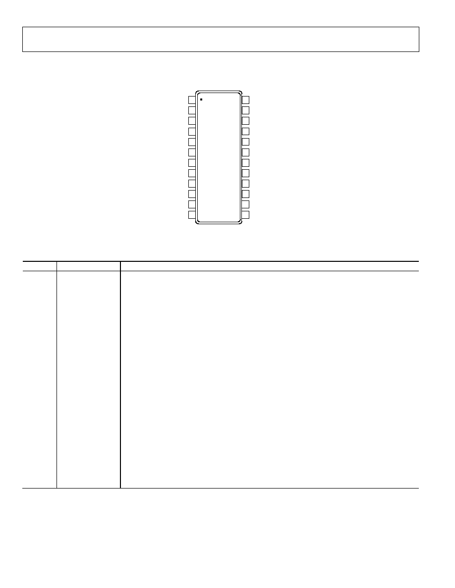
PIN CONFIGURATION AND FUNCTION DESCRIPTIONS
055
27-
00
3
1
2
3
4
5
6
7
8
9
10
20
21
22
23
24
19
18
17
16
15
14
13
12
11
DISABLE
Y1/G1
GND
Pr1/R1
GND
Pb1/B1
LEVEL1
G_SEL
VCC
Y/G_OUT
VEE
Pb/B_OUT
VEE
F_SEL_A
F_SEL_B
Pb2/B2
DGND
Y2/G2
Pr/R_OUT
VCC
DGND
Pr2/R2
MUX
LEVEL2
ADA4411-3
TOP VIEW
(Not to Scale)
Figure 3. 24-Lead QSOP Pin Configuration
Table 5. 24-Lead QSOP Pin Function Descriptions
Pin No.
Name
Description
1
LEVEL1
DC Level Adjust Pin 1
2 DISABLE
Disable/Power
Down
3
Y1/G1
Channel 1 Y/G Video Input
4
GND
Signal Ground Reference
5
Pb1/B1
Channel 1 Pb/B Video Input
6
GND
Signal Ground Reference
7
Pr1/R1
Channel 1 Pr/R Video Input
8
F_SEL_A
Filter Cutoff Select Input A
9
F_SEL_B
Filter Cutoff Select Input B
10
Y2/G2
Channel 2 Y/G Video Input
11
DGND
Digital Ground Reference
12
Pb2/B2
Channel 2 Pb/B Video Input
13
DGND
Digital Ground Reference
14
Pr2/R2
Channel 2 Pr/R Video Input
15
MUX
Input Mux Select Line
16
VCC
Positive Power Supply
17 Pr/R_OUT
Pr/R
Video
Output
18 VEE
Negative
Power
Supply
19 Pb/B_OUT
Pb/B
Video
Output
20 VEE
Negative
Power
Supply
21 Y/G_OUT
Y/G
Video
Output
22
VCC
Positive Power Supply
23 G_SEL
Gain
Select
24
LEVEL2
DC Level Adjust Pin 2
ADA4411-3
Rev. 0 | Page 7 of 16
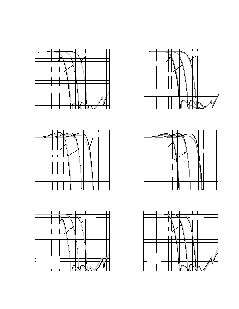
TYPICAL PERFORMANCE CHARACTERISTICS
Unless otherwise noted, G = ×2, R
L
= 150 , V = 1.4 V p-p, V = 5 V, T = 25°C.
O
S
A
05527-
007
FREQUENCY (MHz)
GA
IN
(
d
B
)
1
10
100
45
42
39
36
33
30
27
24
21
18
15
12
9
6
3
0
3
6
15
12
9
F
C
= 9MHz
F
C
= 18MHz
F
C
= 36MHz
BLACK LINE: V
S
= +5V
GRAY LINE: V
S
= ±5V
05527-
004
FREQUENCY (MHz)
GA
IN
(
d
B
)
1
10
100
48
45
42
39
36
33
30
27
24
21
18
15
12
9
6
3
0
3
6
9
F
C
= 9MHz
F
C
= 18MHz
F
C
= 36MHz
BLACK LINE: V
S
= +5V
GRAY LINE: V
S
= ±5V
Figure 4. Frequency Response vs. Power Supply and
Cutoff Frequency (G = ×2)
Figure 7. Frequency Response vs. Power Supply and
Cutoff Frequency (G = ×4)
05
527-
005
FREQUENCY (MHz)
G
A
IN
(
d
B
)
1
10
3.0
3.5
4.0
4.5
5.0
5.5
6.0
6.5
100
BLACK LINE: V
S
= +5V
GRAY LINE: V
S
= ±5V
F
C
= 9MHz
F
C
= 18MHz
F
C
= 36MHz
05
527-
008
FREQUENCY (MHz)
G
A
IN
(
d
B
)
1
10
9.0
12.5
12.0
11.5
11.0
10.5
10.0
9.5
100
F
C
= 9MHz
F
C
= 18MHz
F
C
= 36MHz
BLACK LINE: V
S
= +5V
GRAY LINE: V
S
= ±5V
Figure 5. Frequency Response Flatness vs. Power Supply and
Cutoff Frequency (G = ×2)
Figure 8. Frequency Response Flatness vs. Power Supply and Cutoff Frequency
(G = ×4)
05
527-
006
FREQUENCY (MHz)
G
A
IN
(
d
B
)
1
10
100
48
45
42
39
36
33
30
27
24
21
18
15
12
9
6
3
0
3
6
9
F
C
= 9MHz
F
C
= 18MHz
F
C
= 36MHz
BLACK LINE:
V
OUT
= 100mV p-p
GRAY LINE:
V
OUT
= 2V p-p
0
5527-
00
9
FREQUENCY (MHz)
GA
IN
(
d
B
)
1
10
100
48
45
42
39
36
33
30
27
24
21
18
15
12
9
6
3
0
3
6
9
F
C
= 36MHz
40
°
C
+25
°
C
+85
°
C
F
C
= 9MHz
F
C
= 18MHz
Figure 9. Frequency Response vs. Temperature and Cutoff Frequency
Figure 6. Frequency Response vs. Cutoff Frequency and Output Amplitude

ADA4411-3
Rev. 0 | Page 8 of 16
0
5527-
01
0
FREQUENCY (MHz)
GR
OU
P
D
E
LA
Y
(
n
s
)
1
10
10
100
90
80
70
60
50
40
30
20
100
F
C
= 9MHz
F
C
= 18MHz
F
C
= 36MHz
BLACK LINE: V
S
= +5V
GRAY LINE: V
S
= ±5V
05
52
7
-
01
3
OU
TP
U
T
V
O
LTA
G
E
(
V
)
ER
R
O
R
(
%
)
1.5
1.7
1.9
2.1
2.3
2.5
2.7
2.9
3.1
3.3
3.5
2.5
2.0
1.5
1.0
0.5
0
0.5
1.0
1.5
2.0
2.5
50ns/DIV
2 × INPUT
OUTPUT
ERROR
1% (58ns)
0.5% (70ns)
Figure 13. Settling Time
Figure 10. Group Delay vs. Frequency, Power Supply, and Cutoff Frequency
0
5527-
01
2
FREQUENCY (MHz)
M
UX
I
S
O
L
AT
I
O
N RE
F
E
RRE
D T
O
I
N
P
UT
(
d
B)
0.1
1
10
100
110
100
90
80
70
60
50
40
F
C
= 9MHz
F
C
= 18MHz
F
C
= 36MHz
R
SOURCE
= 300
UNSELECTED MUX IS DRIVEN
05
527-
011
FREQUENCY (MHz)
CRO
S
S
T
AL
K R
E
F
E
R
RE
D T
O
I
N
P
UT
(
d
B)
0.1
1
10
100
110
100
90
80
70
60
50
40
30
F
C
= 9MHz
F
C
= 18MHz
F
C
= 36MHz
R
SOURCE
= 300
Y AND Pr SOURCE CHANNELS
Pb RECEPTOR CHANNEL
Figure 11. Channel-to-Channel Crosstalk vs. Frequency and Cutoff Frequency
Figure 14. MUX Isolation vs. Frequency and Cutoff Frequency
05
52
7-
01
5
OU
TP
U
T V
O
LTA
G
E
(
V
)
1.5
1.7
1.9
2.1
2.3
2.5
2.7
2.9
3.1
3.3
3.5
100ns/DIV
F
C
= 9MHz
F
C
= 18MHz
F
C
= 36MHz
05
52
7-
0
14
OU
TP
U
T V
O
LTA
G
E
(
V
)
1.5
1.7
1.9
2.1
2.3
2.5
2.7
2.9
3.1
3.3
3.5
100ns/DIV
F
C
= 9MHz
F
C
= 18MHz
F
C
= 36MHz
Figure 15. Transient Response vs. Cutoff Frequency (G = ×4)
Figure 12. Transient Response vs. Cutoff Frequency (G = ×2)

ADA4411-3
Rev. 0 | Page 9 of 16
05
52
7-
01
7
FREQUENCY (MHz)
PS
R
R
REF
E
RR
ED T
O
I
N
P
U
T
(
d
B)
0.1
1
10
100
75
65
55
45
35
25
15
5
5
F
C
= 9MHz
F
C
= 18MHz
F
C
= 36MHz
05
52
7-
01
6
FREQUENCY (MHz)
P
S
R
R RE
F
E
RRE
D T
O
I
NP
U
T
(
d
B)
0.1
1
10
100
75
65
55
45
35
25
15
5
5
F
C
= 9MHz
F
C
= 18MHz
F
C
= 36MHz
Figure 16. Positive Supply PSRR vs. Frequency and Cutoff Frequency
Figure 18. Negative Supply PSRR vs. Frequency and Cutoff Frequency
05
52
7-
0
22
OU
TP
U
T V
O
LTA
G
E
(
V
)
1
6
5
4
3
2
1
0
200ns/DIV
2
×
INPUT
F
C
= 36MHz
F
C
= 18MHz
F
C
= 9MHz
055
27
-
0
51
MINIMUM-LOSS MATCHING NETWORK LOSS CALIBRATED OUT
50
118
R
L
= 150
50
86.6
50
NETWORK
ANALYZER Tx
NETWORK
ANALYZER Rx
DUT
Figure 19. Basic Test Circuit for Swept Frequency Measurements
Figure 17. Overdrive Recovery vs. Cutoff Frequency

ADA4411-3
Rev. 0 | Page 10 of 16
THEORY OF OPERATION
The ADA4411-3 is an integrated video filtering and driving
solution that offers variable bandwidth to meet the needs of a
number of different video resolutions. There are three filters,
targeted for use with component video signals. The filters
have selectable bandwidths that correspond to the popular
component video standards. Each filter has a sixth-order
Butterworth response that includes group delay optimization.
The group delay variation from 1 MHz to 36 MHz in the
36 MHz section is 7 ns, which produces a fast settling pulse
response.
The ADA4411-3 is designed to operate in many video
environments. The supply range is 5 V to 12 V, single supply or
dual supply, and requires a relatively low nominal quiescent
current of 15 mA per channel. In single-supply applications,
the PSRR is greater than 60 dB, providing excellent rejection
in systems with supplies that are noisy or under-regulated. In
applications where power consumption is critical, the part
can be powered down to draw typically 15 A by pulling the
DISABLE pin to the most positive rail. The ADA4411-3 is also
well-suited for high encoding frequency applications because it
maintains a stop-band attenuation of more than 40 dB to 400 MHz.
The ADA4411-3 is intended to take dc-coupled inputs
from an encoder or other ground referenced video signals.
The ADA4411-3 input is high impedance. No minimum or
maximum input termination is required, though input
terminations above 1 k can degrade crosstalk performance
at high frequencies. No clamping is provided internally. For
applications where dc restoration is required, dual supplies
work best. Using a termination resistance of less than a few
hundred ohms to ground on the inputs and suitably adjusting
the level-shifting circuitry provides precise placement of the
output voltage.
For single-supply applications (V
S-
= GND), the input voltage
range extends from 100 mV below ground to within 2.0 V of
the most positive supply. Each filter section has a 2:1 input
multiplexer that includes level-shifting circuitry. The level-
shifting circuitry adds a dc component to ground-referenced
input signals so that they can be reproduced accurately without
the output buffers hitting the negative rail. Because the filters
have negative rail input and rail-to-rail output, dc level shifting
is generally not necessary, unless accuracy greater than that of
the saturated output of the driver is required at the most
negative edge. This varies with load but is typically 100 mV
in a dc-coupled, single-supply application. If ac coupling is
used, the saturated output level is higher because the drivers
have to sink more current on the low side. If dual supplies are
used (V
S-
< GND), no level shifting is required. In dual-supply
applications, the level-shifting circuitry can be used to take a
ground referenced signal and put the blanking level at ground
while the sync level is below ground.
The output drivers on the ADA4411-3 have rail-to-rail output
capabilities. They provide either 6 dB or 12 dB of gain with
respect to the ground pins. Gain is controlled by the external
gain select pin. Each output is capable of driving two ac- or dc-
coupled 75 source-terminated loads. If a large dc output level
is required while driving two loads, ac coupling should be used
to limit the power dissipation.
Input MUX isolation is primarily a function of the source
resistance driving into the ADA4411-3. Higher resistances
result in lower isolation over frequency, while a low source
resistance, such as 75 , has the best isolation performance.
See Figure 14 for the MUX isolation performance.
ADA4411-3
Rev. 0 | Page 11 of 16
APPLICATIONS
OVERVIEW
CUTOFF FREQUENCY SELECTION
With its high impedance multiplexed inputs and high output
drive, the ADA4411-3 is ideally suited to video reconstruction
and antialias filtering applications. The high impedance inputs
give designers flexibility with regard to how the input signals
are terminated. Devices with DAC current source outputs that
feed the ADA4411-3 can be loaded in whatever resistance
provides the best performance, and devices with voltage outputs
can be optimally terminated as well. The ADA4411-3 outputs
can each drive up to two source-terminated 75 loads and can
therefore directly drive the outputs from set-top boxes, DVD
players, and the like without the need for a separate output
buffer.
Four combinations of cutoff frequencies are provided for the
video signals. The cutoff frequencies have been selected to
correspond with the most commonly deployed component
video scanning systems. Selection between the cutoff frequency
combinations is controlled by the logic signals applied to the
F_SEL_A and F_SEL_B inputs. Table 7 summarizes cutoff
frequency selection.
Table 7. Filter Cutoff Frequency Selection
F_SEL_A
F_SEL_B
Y/G Cutoff
Pb/B Cutoff
Pr/R Cutoff
0
0
36 MHz
36 MHz
36 MHz
Binary control inputs are provided to select cutoff frequency,
throughput gain, and input signal. These inputs are compatible
with 3 V and 5 V TTL and CMOS logic levels referenced to
GND. The disable feature is asserted by pulling the DISABLE
pin to the positive supply.
The LEVEL1 and LEVEL2 inputs comprise a differential input
that controls the dc level at the output pins.
MULTIPLEXER SELECT INPUTS
Selection between the two multiplexer inputs is controlled by
the logic signals applied to the MUX inputs. Table 6
summarizes the multiplexer operation.
THROUGHPUT GAIN
The throughput gain of the ADA4411-3 signal paths can
be either × 2 or × 4. Gain selection is controlled by the logic
signal applied to the G_SEL pin. Table 6 summarizes how the
gain is selected.
DISABLE
The ADA4411-3 includes a disable feature that can be used
to save power when a particular device is not in use. As
indicated in the Overview section, the disable feature is
asserted by pulling the DISABLE pin to the positive supply.
Table 6 summarizes the disable feature operation. The
DISABLE pin also functions as a reference level for the logic
inputs and therefore must be connected to ground when the
device is not disabled.
Table 6. Logic Pin Function Description
DISABLE MUX
G_SEL
V
S+
= Disabled
1 = Channel 1 Selected
1 = ×2 Gain
GND = Enabled
0 = Channel 2 Selected
0 = ×4 Gain
0
1
36 MHz
18 MHz
18 MHz
1
0
18 MHz
18 MHz
18 MHz
1
1
9 MHz
9 MHz
9 MHz
OUTPUT DC OFFSET CONTROL
The LEVEL1 and LEVEL2 inputs work as a differential, input-
referred output offset control. In other words, the output offset
voltage of a given channel is equal to the difference in voltage
between the LEVEL1 and LEVEL2 inputs, multiplied by the
overall filter gain. This relationship is expressed in Equation 1.
(1)
)
)(
(
)
(
G
LEVEL
LEVEL
OUT
V
OS
2
1
-
=
LEVEL1 and LEVEL2 are the voltages applied to the respective
inputs, and G is the throughput gain.
For example, with the G_SEL input set for ×2 gain, setting
LEVEL1 to 300 mV and LEVEL2 to 0 V shifts the offset voltages
at the ADA4411-3 outputs to 600 mV. This particular setting
can be used in most single-supply applications to keep the
output swings safely above the negative supply rail.
The maximum differential voltage that can be applied across the
LEVEL1 and LEVEL2 inputs is ±500 mV. From a single-ended
standpoint, the LEVEL1 and LEVEL2 inputs have the same
range as the filter inputs. See the Specifications tables for the
limits. The LEVEL1 and LEVEL2 inputs must each be bypassed
to GND with a 0.1 F ceramic capacitor.
In single-supply applications, a positive output offset must be
applied to keep the negative-most excursions of the output
signals above the specified minimum output swing limit.
ADA4411-3
Rev. 0 | Page 12 of 16
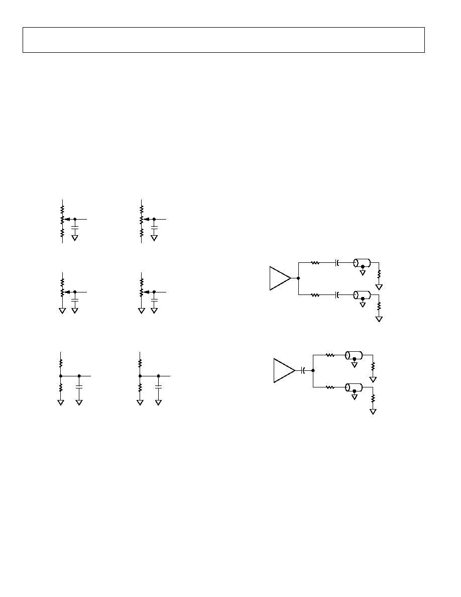
Figure 20 and Figure 21 illustrate several ways to use the
LEVEL1 and LEVEL2 inputs.
INPUT AND OUTPUT COUPLING
Figure 20 shows examples of how
to generate fully adjustable LEVEL1 and LEVEL2 voltages from
±5 V and single +5 V supplies. These circuits show a general
case, but a more practical approach is to fix one voltage and
vary the other.
Inputs to the ADA4411-3 are normally dc-coupled. Ac coupling
the inputs is not recommended; however, if ac coupling is
necessary, suitable circuitry must be provided following the ac
coupling element to provide proper dc level and bias currents at
the ADA4411-3 input stages. The ADA4411-3 outputs can be
either ac- or dc-coupled.
Figure 21 illustrates an effective way to produce
a 600 mV output offset voltage in a single-supply application.
Although the LEVEL2 input could simply be connected to
GND, Figure 21 includes bypassed resistive voltage dividers for
each input so that the input levels can be changed, if necessary.
Additionally, many in-circuit testers require that I/O signals not
be tied directly to the supplies or GND. DNP indicates do not
populate.
When driving single ac-coupled loads in standard 75 video
distribution systems, 220 F coupling capacitors are recom-
mended for use on all but the chrominance signal output. Since
the chrominance signal is a narrow-band modulated carrier, it
has no low frequency content and can therefore be coupled with
a 0.1 F capacitor.
05527-
018
DUAL SUPPLY
0.1
F
LEVEL1
9.53k
1k
9.53k
+5V
5V
0.1
F
LEVEL2
9.53k
1k
9.53k
+5V
5V
SINGLE SUPPLY
0.1
F
LEVEL1
1k
9.09k
+5V
0.1
F
LEVEL2
1k
9.09k
+5V
There are two ac coupling options when driving two loads from
one output. One simply uses the same value capacitor on the
second load, while the other is to use a common coupling
capacitor that is at least twice the value used for the single load
(see Figure 22 and Figure 23).
05
527-
02
0
75
ADA4411-3
75
220
F
220
F
75
75
75
CABLE
75
CABLE
Figure 20. Generating Fully Adjustable Output Offsets
Figure 22. Driving Two AC-Coupled Loads with Two Coupling Capacitors
0552
7-
021
75
75
75
75
470
F
75
CABLE
75
CABLE
ADA4411-3
05527-
019
0.1
F
LEVEL1
634
10k
+5V
DNP
LEVEL2
0
DNP
+5V
Figure 21. Flexible Circuits to Set the LEVEL1 and LEVEL2 Inputs to
Obtain a 600 mV Output Offset on a Single Supply
Figure 23. Driving Two AC-Coupled Loads with One Common Coupling Capacitor
When driving two parallel 150 loads (75 effective load),
the 3 dB bandwidth of the filters typically varies from that of
the filters with a single 150 load. For the 9 MHz and 18 MHz
filters, the typical variation is within ±1.0%; for the 36 MHz
filters, the typical variation is within ±2.5%.

ADA4411-3
Rev. 0 | Page 13 of 16
PRINTED CIRCUIT BOARD LAYOUT
As with all high speed applications, attention to printed
circuit board layout is of paramount importance. Standard high
speed layout practices should be adhered to when designing
with the ADA4411-3. A solid ground plane is recommended,
and surface-mount, ceramic power supply decoupling
capacitors should be placed as close as possible to the supply
pins. All of the ADA4411-3 GND pins should be connected to
the ground plane with traces that are as short as possible.
Controlled impedance traces of the shortest length possible
should be used to connect to the signal I/O pins and should not
pass over any voids in the ground plane. A 75 impedance
level is typically used in video applications. All signal outputs of
the ADA4411-3 should include series termination resistors
when driving transmission lines.
When the ADA4411-3 receives its inputs from a device
with current outputs, the required load resistor value for
the output current is often different from the characteristic
impedance of the signal traces. In this case, if the intercon-
nections are sufficiently short (<< 0.1 wavelength), the trace
does not have to be terminated in its characteristic impedance.
Traces of 75 can be used in this instance, provided their
lengths are an inch or two at the most. This is easily achieved
because the ADA4411-3 and the device feeding it are usually
adjacent to each other, and connections can be made that are
less than one inch in length.
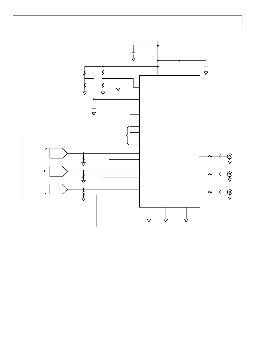
VIDEO ENCODER RECONSTRUCTION FILTER
The ADA4411-3 is easily applied as a reconstruction filter at
the DAC outputs of a video encoder. Figure 24 illustrates how to
use the ADA4411-3 in this type of application with an ADV7322
video encoder in a single-supply application with ac-coupled
outputs.
ADA4411-3
Rev. 0 | Page 14 of 16
Y1/G1
Y2/G2
3
10
Pb1/B1
Pb2/B2
5
12
Pr1/R1
Pr2/R2
7
14
5V
(ANALOG)
LEVEL1
LEVEL2
VCC
16
1
24
G_SEL
23
DISABLE
2
MUX
15
F_SEL_A
8
F_SEL_B
9
BINARY
CONTROL
INPUTS
GND
4, 6
VEE
18, 20
21
Y/G_OUT
19
Pb/B_OUT
17
Pr/R_OUT
0.1
F
22
VCC
ADA4411-3
CHANNEL 2
VIDEO
INPUTS
DGND
11, 13
ADV7322
VIDEO ENCODER
VIDEO
DAC
OUTPUTS
R
L
R
L
R
L
0.1
F
0.1
F
0.1
F
10k
DNP
0
634
75
220
F
75
220
F
75
220
F
05527-
024
Figure 24. The ADA4411-3 Applied as a Single-Supply Reconstruction Filter Following the ADV7322

ADA4411-3
Rev. 0 | Page 15 of 16
OUTLINE DIMENSIONS
24
13
12
1
0.236
BSC
PIN 1
0.154
BSC
SEATING
PLANE
0.010
0.004
0.012
0.008
0.025
BSC
0.069
0.053
0.010
0.006
0.050
0.016
8°
0°
0.065
0.049
COPLANARITY
0.004
0.341
BSC
COMPLIANT TO JEDEC STANDARDS MO-137AE
Figure 25. 24-Lead Shrink Small Outline Package [QSOP]
(RQ-24)
Dimensions shown in inches
ORDERING GUIDE
Model
Temperature Range
Package Description
Order Quantity
Package Option
ADA4411-3ARQZ
40°C to +85°C
24-Lead QSOP
1
RQ-24
1
ADA4411-3ARQZ-R7
40°C to +85°C
24-Lead QSOP
1,000
RQ-24
1
ADA4411-3ARQZ-RL
40°C to +85°C
24-Lead QSOP
2,500
RQ-24
1
1
Z = Pb-free part.

ADA4411-3
Rev. 0 | Page 16 of 16
NOTES
© 2005 Analog Devices, Inc. All rights reserved. Trademarks and
registered trademarks are the property of their respective owners.
D0552707/05(0)