Document Outline
- FEATURES
- APPLICATIONS
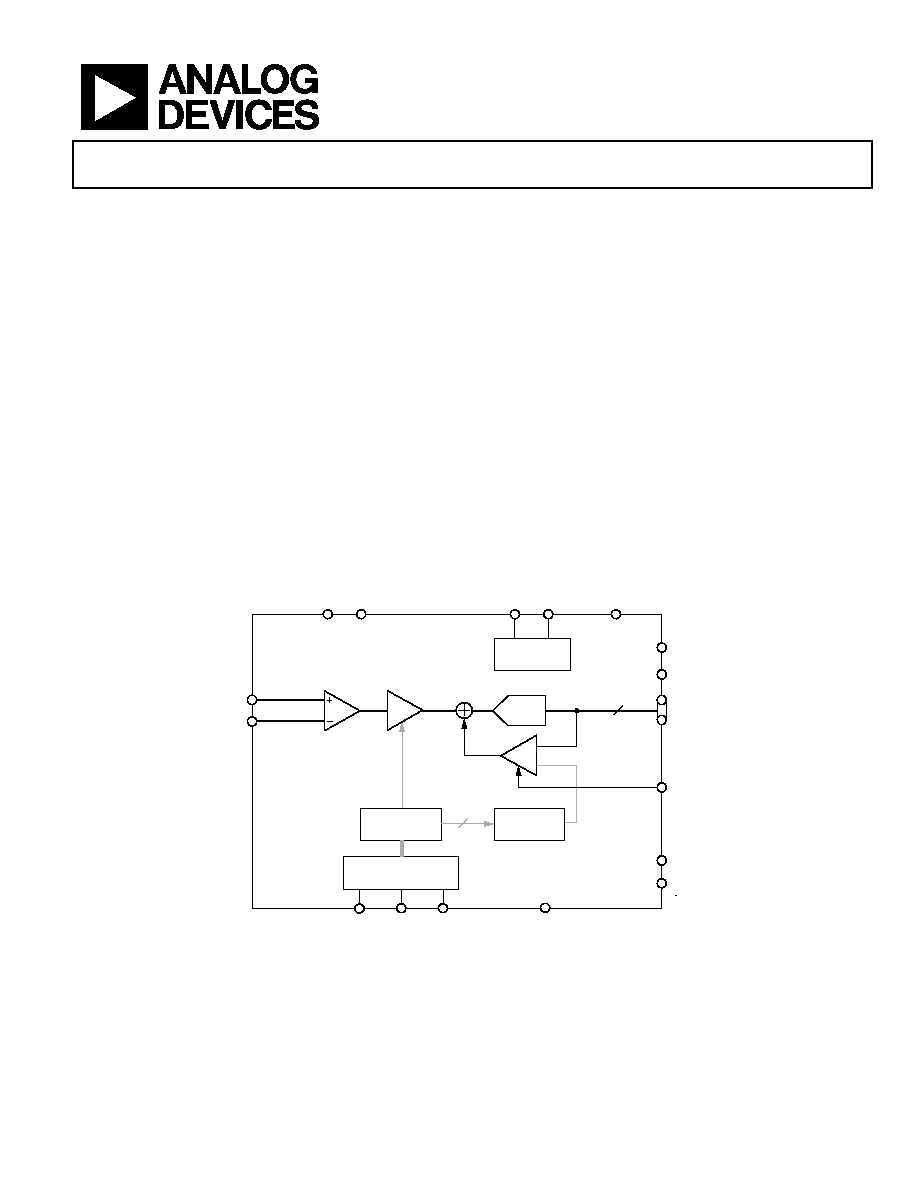
- FUNCTIONAL BLOCK DIAGRAM
- GENERAL DESCRIPTION
- ţ˙
- ţ˙
- ţ˙
- ţ˙
- ţ˙
- ţ˙
- ţ˙
- ţ˙
- VARIABLE GAIN AMPLIFIER
- ţ˙
- OPTICAL BLACK CLAMP
- ţ˙
- ţ˙
Complete 14-Bit, 56 MSPS
Imaging Signal Processor
AD9941
Rev. 0
Information furnished by Analog Devices is believed to be accurate and reliable.
However, no responsibility is assumed by Analog Devices for its use, nor for any
infringements of patents or other rights of third parties that may result from its use.
Specifications subject to change without notice. No license is granted by implication
or otherwise under any patent or patent rights of Analog Devices. Trademarks and
registered trademarks are the property of their respective owners.
One Technology Way, P.O. Box 9106, Norwood, MA 02062-9106, U.S.A.
Tel: 781.329.4700
www.analog.com
Fax: 781.461.3113
© 2005 Analog Devices, Inc. All rights reserved.
FEATURES
Differential sensor input with 1 V p-p input range
0 dB/6 dB variable gain amplifier (VGA)
Low noise optical black clamp circuit
14-bit, 56 MSPS analog-to-digital converter (ADC)
No missing codes guaranteed
3-wire serial digital interface
3 V single-supply operation
Low power CMOS: 145 mW @ 3.0 V, 56 MHz
48-lead LQFP package
APPLICATIONS
Digital still cameras using CMOS imagers
Professional HDTV camcorders
Professional/high-end digital cameras
Broadcast cameras
GENERAL DESCRIPTION
The AD9941 is a complete analog signal processor for imaging
applications that do not require correlated double sampling
(CDS). It is also suitable for processing the output signal from
the AD9940 CDS front end product. It features a 56 MHz, single-
channel architecture designed to sample and condition the output
of CMOS imagers and CCD arrays already containing on-chip
CDS. The AD9941 signal chain consists of a differential input
sample-and-hold amplifier (SHA), a digitally controlled variable
gain amplifier (VGA), a black level clamp, and a 14-bit ADC.
The internal registers are programmed through a 3-wire serial
digital interface.
The AD9941 operates from a single 3 V supply, typically
dissipates 145 mW, and is packaged in a 48-lead LQFP.
FUNCTIONAL BLOCK DIAGRAM
ADCLK
BAND GAP
REFERENCE
DOUT
PBLK
REFT
REFB
0dB, 6dB
VIN+
DVDD
DVSS
VIN
DRVDD
DRVSS
DIGITAL
INTERFACE
SDATA
SCK
SL
CLPOB
14
VGA
CLP
AD9941
8
INTERNAL
REGISTERS
BLK CLAMP
LEVEL
14-BIT
ADC
AVDD AVSS
05504-001
SHA
Figure 1.

AD9941
Rev. 0 | Page 2 of 16
TABLE OF CONTENTS
Specifications .....................................................................................3
Digital Specifications ....................................................................3
Analog Specifications ...................................................................4
Timing Specifications ...................................................................5
Timing Diagrams ..........................................................................5
Absolute Maximum Ratings ............................................................6
Thermal Characteristics...............................................................6
ESD Caution ..................................................................................6
Pin Configuration and Function Descriptions .............................7
Terminology.......................................................................................8
Equivalent Input/Output Circuits...................................................9
Serial Interface Timing...................................................................10
Circuit Description and Operation ..............................................12
Differential Input SHA ...............................................................12
Variable Gain Amplifier .............................................................13
ADC..............................................................................................13
Optical Black Clamp...................................................................13
Applications Information...............................................................14
Outline Dimensions........................................................................16
Ordering Guide ...........................................................................16
REVISION HISTORY
7/05--Revision 0: Initial Version

AD9941
Rev. 0 | Page 3 of 16
SPECIFICATIONS
Table 1.
Parameter
Min
Typ
Max
Unit
TEMPERATURE RANGE
Operating
-25
+85
°C
Storage
-65
+150
°C
POWER SUPPLY VOLTAGE
AVDD, DVDD, DRVDD
2.9
3.0
3.6
V
POWER DISSIPATION
Normal Operation--56 MHz, AVDD = DVDD = DRVDD = 3.0 V
145
mW
Standby Mode
2
mW
MAXIMUM CLOCK RATE
56
MHz
DIGITAL SPECIFICATIONS
DRVDD = 2.9 V, C
L
= 20 pF, unless otherwise noted.
Table 2.
Parameter
Symbol
Min
Typ
Max
Unit
LOGIC INPUTS
High Level Input Voltage
V
IH
2.1
V
Low Level Input Voltage
V
IL
0.6
V
High Level Input Current
I
IH
10
A
Low Level Input Current
I
IL
10
A
Input Capacitance
C
IN
10
pF
LOGIC OUTPUTS
High Level Output Voltage , I
OH
= 2 mA
V
OH
2.2
V
Low Level Output Voltage , I
OL
= 2 mA
V
OL
0.5
V

AD9941
Rev. 0 | Page 4 of 16
ANALOG SPECIFICATIONS
T
MIN
to T
MAX
, AVDD = DVDD, f
ADCLK
= 56 MHz,
unless otherwise noted.
Table 3.
Parameter
Min
Typ
Max
Unit
Notes
ANALOG INPUTS (VIN+, VIN-)
Input Common-Mode Range
1
1.1
2.3
V
Linear operating range for VIN+, VIN-
Maximum Input Amplitude
1
1.0
V p-p
VIN+ and VIN- signal swing
Maximum Differential Input Amplitude
1
2.0
V p-p
Defined as VIN+ - VIN-
OB Correction Range
OB offset shown in Note 1
Gain 1 (6 dB)
1
±90 mV
Gain 2 (0 dB)
1
±180
mV
VARIABLE GAIN AMPLIFIER (VGA)
Gain Control Resolution
2
Steps
Gain Range
CCD Mode Gain 1
5.0
5.5
6.0
dB
CCD Mode Gain 2
-0.5
0
+0.5
dB
BLACK LEVEL CLAMP
Clamp Level Resolution
256
Steps
Clamp Level
Clamp level = 4 × REFBLK
Minimum Clamp Level (Code 0)
0
LSB
Maximum Clamp Level (Code 255)
1020
LSB
A/D CONVERTER
Resolution 14
Bits
Differential Nonlinearity (DNL)
±0.5
LSB
No Missing Codes
Guaranteed
Integral Nonlinearity
0.3
% FS
Full-Scale Input Voltage
2.0
V p-p
VOLTAGE REFERENCE
Reference Top Voltage (REFT)
2.0
V
Reference Bottom Voltage (REFB)
1.0
V
1
Input signal characteristics defined as
05504-002
2.3V
1V p-p MAX INPUT SIGNAL SWING, VIN+ AND VIN
2V p-p MAX DIFFERENTIAL SIGNAL, VIN+ VIN
1.1V
VIN+
GND
VIN
BLACK
LEVEL
WHITE
LEVEL
MAX OB OFFSET
AD9941
Rev. 0 | Page 5 of 16
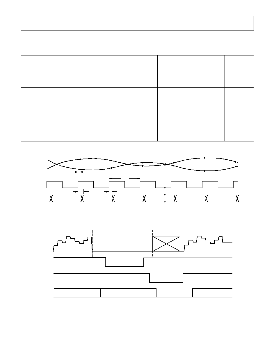
TIMING SPECIFICATIONS
C
L
= 20 pF, f
ADCLK
= 56 MHz, refer to Figure 2 and Figure 8.
Table 4.
Parameter
Symbol
Min
Typ
Max
Unit
SAMPLE CLOCKS
ADCLK Clock Period
18
ns
ADCLK High/Low Pulse Width
8
ns
CLPOB Pulse Width
20
Pixels
Internal Clock Delay
T
ID
3
ns
DATA OUTPUTS
Output Delay
T
OD
20
ns
Output Hold Time
T
H
5 ns
Pipeline Delay
9
Cycles
SERIAL INTERFACE
Maximum SCK Frequency
f
SCLK
10
MHz
SL to SCK Setup Time
t
LS
10
ns
SCK to SL Hold Time
t
LH
10
ns
SDATA Valid to SCK Rising Edge Setup
t
DS
10
ns
SCK Rising Edge to SDATA Valid Hold
t
DH
10
ns
TIMING DIAGRAMS
t
OD
t
H
t
ID
t
CONV
NOTES
1. VIN+ AND VIN SIGNALS ARE SAMPLED AT ADCLK RISING EDGES (CAN BE INVERTED USING THE ADCPOL REGISTER).
2. INTERNAL SAMPLING DELAY (APERTURE) t
ID
IS TYPICALLY 3ns.
3. OUTPUT DATA LATENCY IS NINE ADCLK CYCLES.
ADCLK
OUTPUT
DATA
VIN+
N
N + 1
N + 2
N + 8
N + 9
N 10
N 1
N 8
N 9
N
VIN
05504-007
Figure 2. Input/Output Data Timing
IMAGER
SIGNAL
EFFECTIVE PIXELS
CLPOB
OPTICAL BLACK PIXELS
HORIZONTAL
BLANKING
EFFECTIVE PIXELS
PBLK
OUTPUT
DATA
EFFECTIVE PIXEL DATA
OB PIXEL DATA
EFFECTIVE DATA
NOTES
1. CLPOB OVERWRITES PBLK. PBLK DOES NOT AFFECT CLAMP OPERATION IF OVERLAPPING CLPOB.
2. PBLK SIGNAL IS OPTIONAL.
3. DIGITAL OUPUT DATA IS ALL ZEROS DURING PBLK. OUTPUT DATA LATENCY IS NINE ADCLK CYCLES.
05504-008
Figure 3. Typical Imager Timing

AD9941
Rev. 0 | Page 6 of 16
ABSOLUTE MAXIMUM RATINGS
Table 5.
Parameter
Rating
REFT, REFB
AVSS - 0.3 V to AVDD + 0.3 V
VIN+, VIN-
AVSS - 0.3 V to AVDD + 0.3 V
ADCLK, RST, SL, SDI, SCK
DVSS - 0.3 V to DVDD + 0.3 V
AVDD to AVSS
-0.3 V to + 3.9 V
DVDD and DRVDD to DVSS
and DRVSS
-0.3 V to +3.9 V
Any VSS to Any VSS
-0.3 V to +0.3 V
Digital Outputs to DRVSS
-0.3 V to DRVDD + 0.3 V
CLPOB/PBLK to DVSS
-0.3 V to DVDD + 0.3 V
SCK, SL, and SDATA to DVSS
-0.3 V to DVDD + 0.3 V
Stresses above those listed under Absolute Maximum Ratings
may cause permanent damage to the device. This is a stress
rating only; functional operation of the device at these or any
other conditions above those indicated in the operational
section of this specification is not implied. Exposure to absolute
maximum rating conditions for extended periods may affect
device reliability.
THERMAL CHARACTERISTICS
Thermal resistance for the 48-lead LQFP package:
JA
= 92°C/W
1
1
JA
is measured using a 4-layer PCB.
ESD CAUTION
ESD (electrostatic discharge) sensitive device. Electrostatic charges as high as 4000 V readily accumulate on the
human body and test equipment and can discharge without detection. Although this product features
proprietary ESD protection circuitry, permanent damage may occur on devices subjected to high energy
electrostatic discharges. Therefore, proper ESD precautions are recommended to avoid performance
degradation or loss of functionality.
AD9941
Rev. 0 | Page 7 of 16
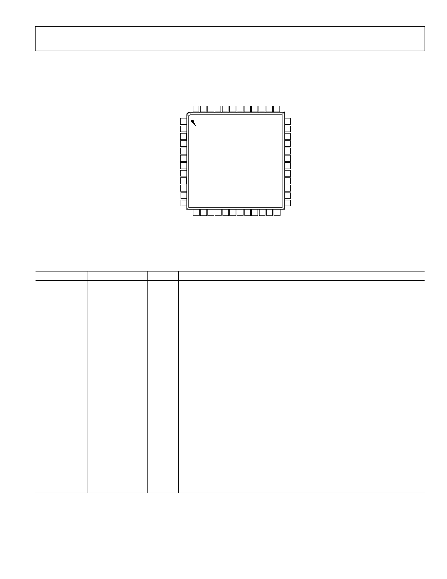
PIN CONFIGURATION AND FUNCTION DESCRIPTIONS
48
D1
47
D0
46
SL
45
SC
K
44
S
DAT
A
43
RS
T
42
D
VSS
41
NC
40
NC
39
RE
FB
38
RE
FT
37
D
VSS
35
AVSS
34
NC
33
AVDD
30
VIN+
31
VIN
32
NC
36
NC
29
NC
28
NC
27
NC
25
NC
26
NC
2
D3
3
D4
4
D5
7
D8
6
D7
5
D6
1
D2
8
D9
9
D10
10
D11
12
D13
11
D12
NC = NO CONNECT
13
DRV
DD
14
D
R
VSS
15
D
VSS
16
ADCLK
17
DV
DD
18
NC
19
PB
LK
20
CLP
O
B
21
NC
22
NC
23
NC
24
NC
PIN 1
AD9941
TOP VIEW
(Not to Scale)
05504-003
Figure 4. Pin Configuration
Table 6. Pin Function Descriptions
Pin No.
Mnemonic
Type
Description
1 to 12
D2 to D13
DO
Digital Data Outputs
13
DRVDD
P
Digital Output Driver Supply
14
DRVSS
P
Digital Output Ground
15
DVSS
P
Digital Ground
16
ADCLK
DI
Digital Data Output Clock
17
DVDD
P
Digital Supply
18, 21 to 29, 32,
34, 36, 40, 41
NC
NC
No Connection (tie to V
DD
or GND)
19
PBLK
DI
Preblanking Clock Input (internal 50 k pull-up)
20
CLPOB
DI
Black Level Clamp Clock Input
30
VIN+
AI
Positive Data Input
31
VIN-
AI
Negative Data Input
33
AVDD
P
Analog Supply
35
AVSS
P
Analog Ground (GND)
37
DVSS
P
Digital Ground
38
REFT
AO
ADC Reference Voltage Top (bypass to GND with a 0.1 F capacitor)
39
REFB
AO
ADC Reference Voltage Bottom (bypass to GND with a 0.1 F capacitor)
42 DVSS P
Digital
Ground
43
RST
DI
Reset Control for Internal Registers (active low)
44
SDATA
DI
Serial Data Input Signal
45
SCK
DI
Serial Clock
46
SL
DI
Serial Load Enable
47
D0
DO
Digital Data Output
48
D1
DO
Digital Data Output

AD9941
Rev. 0 | Page 8 of 16
TERMINOLOGY
Differential Nonlinearity (DNL)
An ideal ADC exhibits code transitions that are exactly 1 LSB
apart. DNL is the deviation from this ideal value; therefore, every
code must have a finite width. No missing codes guaranteed to
14-bit resolution indicates that all 16,384 codes must be present
over all operating conditions.
Peak Nonlinearity
Peak nonlinearity, a full signal chain specification, refers to the
peak deviation of the output of the AD9941 from a true straight
line. The point used as zero scale occurs 0.5 LSB before the first
code transition. Positive full scale is defined as a level 1 LSB and
0.5 LSB beyond the last code transition. The deviation is measured
from the middle of each output code to the true straight line. The
error is then expressed as a percentage of the 2 V ADC full-scale
signal. The input signal is always appropriately gained up to fill
the ADC's full-scale range.
Power Supply Rejection (PSR)
The PSR is measured with a step change applied to the supply
pins. The PSR specification is calculated from the change in the
data outputs for a given step change in the supply voltage.
Total Output Noise
The rms output noise is measured using histogram techniques.
The standard deviation of the ADC output codes is calculated
in LSB and represents the rms noise level of the total signal
chain at the specified gain setting. The output noise can be
converted to an equivalent voltage, using the relationship
1 LSB = (ADC full scale/2
n
codes)
where n is the bit resolution of the ADC, and 1 LSB is
approximately 122 V.
Internal Delay for SHA
The internal delay, or aperture delay, is the time delay from
when the sampling edge is applied to the AD9941 to when the
actual sample of the input signal is held. The ADCLK samples
the input signal during the transition from low to high; therefore,
the internal delay is measured from each clock's rising edge to
the instant the actual sample is taken.

AD9941
Rev. 0 | Page 9 of 16
EQUIVALENT INPUT/OUTPUT CIRCUITS
05504-004
DVDD
DVSS
330
Figure 5. Digital Inputs--ADCLK, CLPOB, PBLK, SCK, SDATA, SL, RST
DVSS
DRVDD
DVSS
DRVSS
DATA
THREE-STATE
DOUT
05504-005
Figure 6. Data Outputs--D0 to D13
60
AVDD
AVSS
AVSS
05504-006
Figure 7. VIN+, VIN-
AD9941
Rev. 0 | Page 10 of 16
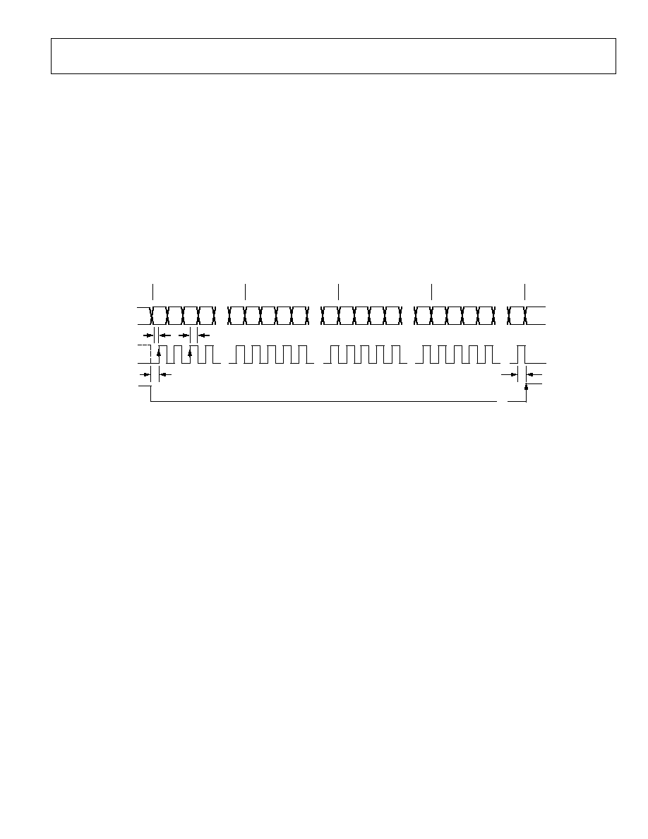
SERIAL INTERFACE TIMING
All of the internal registers of the AD9941 are accessed through
a 3-wire serial interface. Each register consists of an 8-bit data
byte, starting with the LSB bit. As shown in Figure 8, the data
bits are clocked in on the rising edge of SCK after SL is asserted
low, and the entire 8-bit word is latched in on the rising edge of
SL after the last MSB bit. Consecutive serial writes are performed
starting with Address 00 and ending with an address MSB bit
prior to asserting SL high.
Note that Address 00 must be written at the start of any write
operation to specify the PARTSEL bit. The LSB of Address 00
(PARTSEL) must be set high to write to the AD9941 registers.
A hard reset is recommended after power-up to reset the
AD9941 prior to performing a serial interface write. A hard
reset is performed by asserting the RST pin low for a minimum
of 10 s. The serial interface pins SCK, SL, and SDI must be in a
known state after the RST has been applied.
SDATA
SCK
SL
D0
D2
D3
D7 D0
D3
D2
D7
D0
...
...
...
...
ADDR 01
D2
D3
D7
D0
D3
D2
D7
...
...
...
...
...
NOTES
1. ANY NUMBER OF ADJACENT REGISTERS MAY BE LOADED SEQUENTIALLY, BEGINNING WITH THE LOWER ADDRESS 00.
2. WHEN SEQUENTIALLY LOADING MULTIPLE REGISTERS, THE EXACT REGISTER LENGTH (SHOWN ABOVE) MUST BE USED
FOR EACH REGISTER.
3. ALL LOADED REGISTERS ARE SIMULTANEOUSLY UPDATED ON THE RISING EDGE OF SL.
ADDR N
ADDR N + 1
ADDR 00
t
LS
t
LH
t
DH
t
DS
D1
D1
D1
D1
05504-009
Figure 8. Consecutive Serial Write Interface Timing

AD9941
Rev. 0 | Page 11 of 16
Table 7. Serial Interface Registers
Address
Data Bit Content
Default Value
Name
Description
00
[0]
1
PARTSEL
1 = select AD9941, 0 = select AD9940
[2:1]
1
OPERATION MODE
0 = standby mode
1 = 6 dB VGA gain mode
2 = test mode
3 = 0 dB VGA gain mode
[3]
0
TESTMODE
Always set to 0
[4]
0
ADCPOL
0 = ADCLK rising edge update
1 = ADCLK falling edge update
[5]
0
CLPMODE
0 = fast clamp off
1 = fast clamp on (the OB loop time constant is reduced by half)
[6]
0
TESTMODE
Always set to 0
[7]
0
DOUT DISABLE
0 = normal operation, 1 = data outputs are three-state
01
[5:0]
0
TESTMODE
Always set to 0
[6]
CLPDISABLE
0 = OB clamp enabled, 1= OB clamp disabled
[7]
TESTMODE
Always set to 0
02
[7:0]
0
TESTMODE
Always set to 72
03
[7:0]
0
TESTMODE
Always set to 99
04
[7:0]
0
TESTMODE
Always set to 16
05
[0]
0
CLPLEVEL ENABLE
0 = disable CLAMPLEVEL register, clamp level fixed at 492 LSB
1 = enable CLAMPLEVEL register, clamp level is set to value in
Register Value 06 CLAMPLEVEL
[1]
0
CLPUPDATE
0 = ignore new value in CLAMPLEVEL register
1 = update new clamp level value with CLAMPLEVEL register
[7:2]
0
TESTMODE
Always set to 0
06
[7:0]
0
CLAMPLEVEL
OB clamp level (0 = 0 LSB, 123 = 492, 255 = 1020 LSB)
Clamp level (LSB) = 4 × REFBLK
AD9941
Rev. 0 | Page 12 of 16
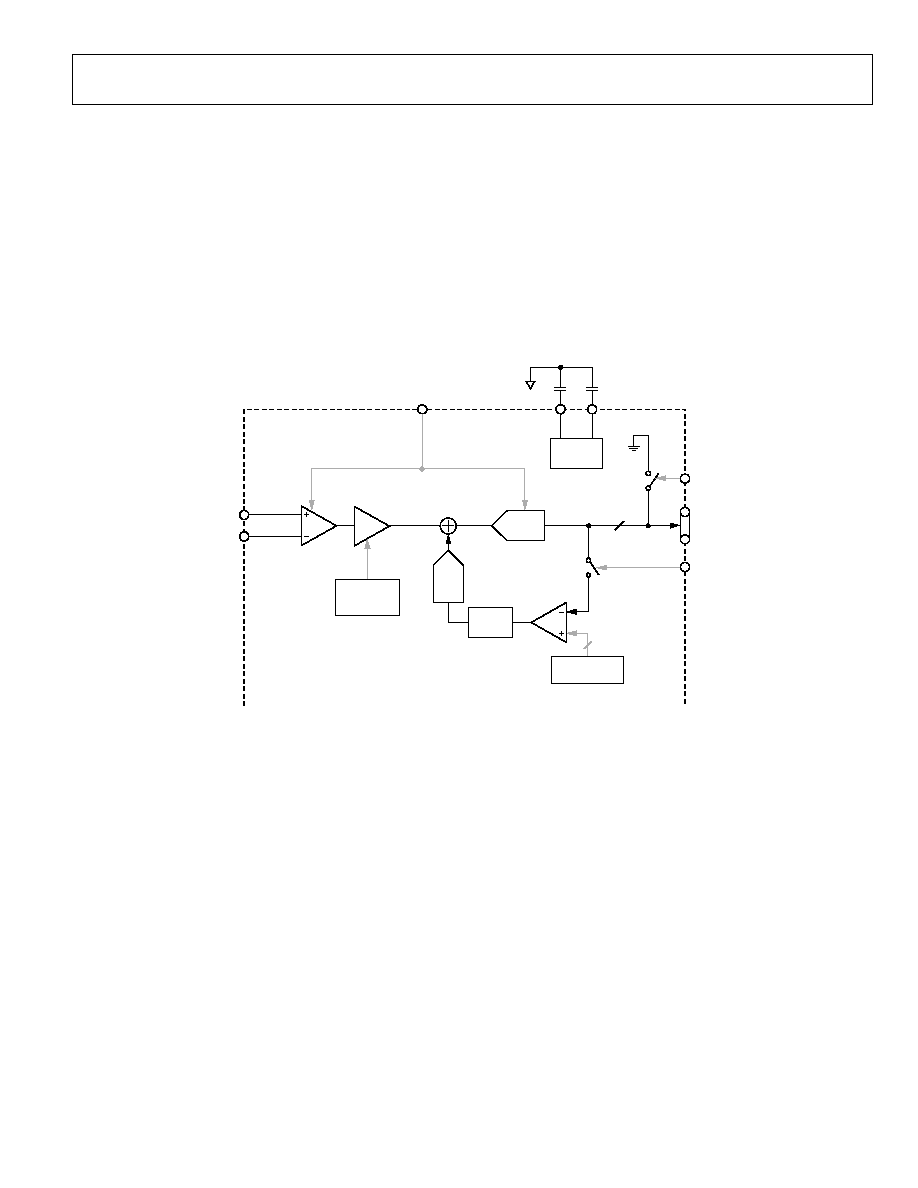
CIRCUIT DESCRIPTION AND OPERATION
The AD9941 signal processing chain is shown in Figure 9. Each
processing step is essential in achieving a high quality image
from the raw data of the imager.
DIFFERENTIAL INPUT SHA
The differential input SHA circuit is designed to accommodate
a variety of image sensor output voltages. The timing shown in
Figure 2 illustrates how the ADCLK signal is used to sample
both VIN+ and VIN- signals simultaneously. The imager's
signal is sampled on the rising edge of ADCLK. Placement of
this clock signal is critical in achieving the best performance
from the imager. An internal ADCLK delay (t
ID
) of 3 ns is caused
by internal propagation delays.
05504-010
DIGITAL
FILTER
CLPOB
OPTICAL BLACK
CLAMP
14-BIT
ADC
8-BIT
DAC
8
SHA
INTERNAL
V
REF
0dB, 6dB
VGA
REFT
REFB
PBLK
1.0V
2.0V
DOUT
AD9941
0.1
F 0.1
F
OPERATION
MODE
REGISTER
CLAMP LEVEL
REGISTER
14
VIN+
ADCLK
VIN
Figure 9. Internal Block Diagram

AD9941
Rev. 0 | Page 13 of 16
VARIABLE GAIN AMPLIFIER
The VGA stage can be programmed to either 0 dB or 6 dB using
the OPERATION MODE register. The 6 dB gain setting is needed
to match a 1 V input signal with the ADC full-scale range of 2 V.
The 0 dB gain setting can be used with the AD9940 CDS front
end component, which has a 2 V differential output range. Note
that the OB correction range is different for each gain setting, as
outlined in Table 3.
ADC
The AD9941 uses a high performance ADC architecture,
optimized for high speed and low power. Differential
nonlinearity (DNL) performance is typically better than
0.5 LSB. The ADC uses a 2 V input range.
OPTICAL BLACK CLAMP
The optical black clamp loop is used to remove residual offsets
in the signal chain and to track low frequency variations in the
imager's black level. During the optical black (shielded) pixel
interval on each line, the ADC output is compared with a fixed
black level reference, selected by the user in the CLAMPLEVEL
register. The value can be programmed between 0 LSB and
1020 LSB in 256 steps. The resulting error signal is filtered to
reduce noise, and the correction value is applied to the ADC
input through a digital-to-analog converter. Normally, the
optical black clamp loop is turned on once per horizontal line,
but this loop can be updated more slowly to suit a particular
application. If external digital clamping is used during the
postprocessing, the AD9941 optical black clamping can be
disabled using the CLPDISABLE register.
The CLPOB pulse should be placed during the imager's optical
black pixels. It is recommended that the CLPOB pulse duration
be at least 20 pixels wide to minimize clamp noise. Shorter pulse
widths can be used, but clamp noise may increase and the
ability to track low frequency variations in the black level will
be reduced.
AD9941
Rev. 0 | Page 14 of 16
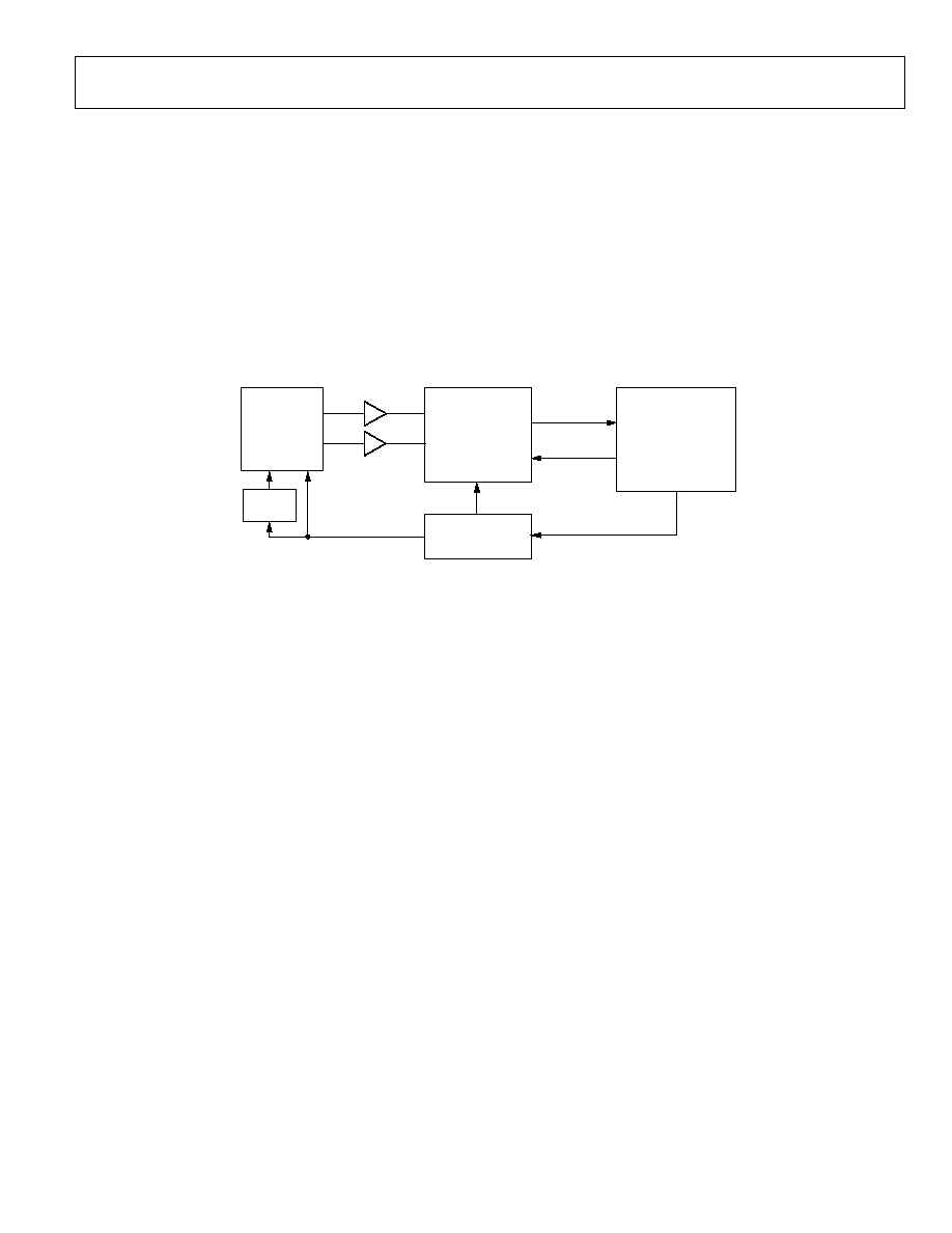
APPLICATIONS INFORMATION
All signals should be carefully routed on the PCB to maintain
low noise performance. The clock inputs are located on the
package side opposite the analog pins and should be connected
to the digital ASIC. A single ground plane is recommended for
the AD9941. This ground plane should be as continuous as
possible, particularly where analog pins are concentrated. This
ensures that all analog decoupling capacitors provide the lowest
possible impedance path between the power and bypass pins
and their respective ground pins. All decoupling capacitors
should be located as close as possible to the package pins.
Careful placement of a split in the ground plane on the board
can help prevent the return current of the horizontal driver
from flowing into the analog ground, thereby reducing digital-
to-analog coupling noise. Power supply decoupling is very
important for achieving low noise performance. Figure 11
shows the local high frequency decoupling capacitors, but
additional capacitance is recommended for lower frequencies.
Additional capacitors and ferrite beads can further reduce noise.
CMOS
OR
CCD
IMAGER
VIN+
OUT+
AD9941
ADC
OUT
REGISTER-
DATA
IMAGER
TIMING
DIGITAL IMAGE
PROCESSING
ASIC
DIGITAL
OUTPUTS
BUFFER
OR
LEVEL SHIFT
TIMING
GENERATOR
V-DRIVER
(CCD)
ADCLK/CLAMP
TIMING
SERIAL
INTERFACE
(MAY ALSO
INCLUDE TG)
VIN
OUT
05504-011
Figure 10. System Application Diagram

AD9941
Rev. 0 | Page 15 of 16
3V
ANALOG
SUPPLY
CLOCK
INPUTS
3V
ANALOG
SUPPLY
3V
DRIVER
SUPPLY
VIN INPUT
VIN+ INPUT
RST
SERIAL
INTERFACE
0.1
F
0.1
F
DATA
OUTPUTS
48
D1
47
D0
46
SL
45
SC
K
44
S
DATA
43
RS
T
42
D
VSS
41
NC
40
NC
39
RE
FB
38
RE
FT
37
D
VSS
35
AVSS
34
NC
33
AVDD
30
VIN+
31
VIN
32
NC
36
NC
29
NC
28
NC
27
NC
25
NC
26
NC
2
D3
3
D4
4
D5
7
D8
6
D7
5
D6
1
D2
8
D9
9
D10
10
D11
12
D13
11
D12
13
DRV
DD
14
D
R
VSS
15
D
VSS
16
ADCLK
17
DV
DD
18
NC
19
PB
LK
20
CLP
O
B
21
NC
22
NC
23
NC
24
NC
PIN 1
AD9941
TOP VIEW
(Not to Scale)
0.1
F
0.1
F
0.1
F
3
14
3
05504-012
Figure 11. Recommended Circuit Configuration

AD9941
Rev. 0 | Page 16 of 16
OUTLINE DIMENSIONS
COMPLIANT TO JEDEC STANDARDS MS-026-BBC
TOP VIEW
(PINS DOWN)
1
12
13
25
24
36
37
48
0.27
0.22
0.17
0.50
BSC
LEAD PITCH
7.00
BSC SQ
1.60
MAX
0.75
0.60
0.45
VIEW A
9.00
BSC SQ
PIN 1
0.20
0.09
1.45
1.40
1.35
0.08 MAX
COPLANARITY
VIEW A
ROTATED 90° CCW
SEATING
PLANE
7°
3.5°
0°
0.15
0.05
Figure 12. 48-Lead Low Profile Quad Flat Package [LQFP]
(ST-48)
Dimensions shown in millimeters
ORDERING GUIDE
Model
Temperature Range
Package Description
Package Option
AD9941BSTZ
1
-25°C to +85°C
48-Lead Low Profile Quad Flat Package (LQFP)
ST-48
AD9941BSTZRL
1
-25°C to +85°C
48-Lead Low Profile Quad Flat Package (LQFP)
ST-48
1
Z = Pb-free part.
© 2005 Analog Devices, Inc. All rights reserved. Trademarks and
registered trademarks are the property of their respective owners.
D0550407/05(0)