Document Outline
- FEATURES
- APPLICATIONS
- GENERAL DESCRIPTION
- PRODUCT HIGHLIGHTS
- ţ˙
- ţ˙
- ţ˙
- ţ˙
- ţ˙
- ţ˙
- ţ˙
- ţ˙
- ţ˙
- ţ˙
- ţ˙

Dual, 12-/14-/16-Bit,
1.0 GSPS D/A Converter
AD9776/AD9778/AD9779
Rev. 0
Information furnished by Analog Devices is believed to be accurate and reliable.
However, no responsibility is assumed by Analog Devices for its use, nor for any
infringements of patents or other rights of third parties that may result from its use.
Specifications subject to change without notice. No license is granted by implication
or otherwise under any patent or patent rights of Analog Devices. Trademarks and
registered trademarks are the property of their respective owners.
One Technology Way, P.O. Box 9106, Norwood, MA 02062-9106, U.S.A.
Tel: 781.329.4700
www.analog.com
Fax: 781.461.3113
© 2005 Analog Devices, Inc. All rights reserved.
FEATURES
DAC output sample rate: 1 GSPS
1.8 V/3.3 V single supply operation
Low power: 1.0 W @ 1 GSPS, 600 mW @ 500 MSPS,
full operating conditions
SFDR = 78 dBc to f
OUT
= 100 MHz
Single carrier WCDMA ACLR = 79 dBc @ 80 MHz IF
CMOS data input interface with adjustable setup and hold
Analog output: adjustable 8.7 mA to 31.7 mA,
RL = 25 to 50
Novel 2×, 4×, and 8× interpolator/coarse complex modulator
allows carrier placement anywhere in DAC bandwidth
Auxiliary DACs allow control of external VGA and offset control
Multiple chip synchronization interface
High performance, low noise PLL clock multiplier
Digital inverse sinc filter
100-lead, exposed paddle TQFP package
APPLICATIONS
Wireless infrastructure
Digital high or low IF synthesis
Internal digital upconversion capability
Transmit diversity
Wideband communications systems
point-to-point wireless, LMDS
Multicarrier WCDMA
Multicarrier GSM
GENERAL DESCRIPTION
The AD9776/AD9778/AD9779 are dual, 12-/14-/16-bit, high
dynamic range DACs that provide a sample rate of 1 GSPS, thus
permitting multicarrier generation up to its Nyquist frequency.
They include features optimized for direct conversion transmit
applications, including complex digital modulation, and gain
and offset compensation. The DAC outputs are optimized to
interface seamlessly with analog quadrature modulators such as
the AD8349. A serial peripheral interface (SPI) provides for
programming/readback of many internal parameters. The
output current can be programmed over a range of 10 mA to
30 mA. The devices are manufactured on an advanced 0.18 m
CMOS process and operate from 1.8 V and 3.3 V supplies for
a total power consumption of 1.0 W. They are enclosed in
100-lead TQFP packages.
PRODUCT HIGHLIGHTS
1.
Ultralow noise and intermodulation distortion (IMD)
enable high quality synthesis of wideband signals from
baseband to high intermediate frequencies.
2.
A proprietary DAC output switching technique enhances
dynamic performance.
3.
The current outputs can be easily configured for various
single-ended or differential circuit topologies.

AD9776/AD9778/AD9779
Rev. 0 | Page 2 of 56
TABLE OF CONTENTS
Functional Block Diagram .............................................................. 3
Specifications..................................................................................... 4
Absolute Maximum Ratings............................................................ 7
ESD Caution.................................................................................. 7
Pin Configurations and Function Descriptions ........................... 8
Typical Performance Characteristics ........................................... 14
Terminology .................................................................................... 22
Theory of Operation ...................................................................... 23
Serial Peripheral Interface ......................................................... 23
MSB/LSB Transfers..................................................................... 24
SPI Register Map............................................................................. 25
Interpolation Filter Architecture .................................................. 29
Interpolation Filter Minimum and Maximum Bandwidth
Specifications .............................................................................. 33
Driving the DACCLK Input ..................................................... 33
Full-Scale Current Generation ................................................. 36
Power Dissipation....................................................................... 37
Power-Down and Sleep Modes................................................. 38
Interleaved Data Mode .............................................................. 39
Timing Information ................................................................... 39
Evaluation Board Operation ......................................................... 45
Modifying the Evaluation Board to Use the AD8349 On-
Board Quadrature Modulator................................................... 47
Evaluation Board Schematics ................................................... 48
Outline Dimensions ....................................................................... 55
Ordering Guide .......................................................................... 55
REVISION HISTORY
7/05--Revision 0: Initial Version
AD9776/AD9778/AD9779
Rev. 0 | Page 3 of 56
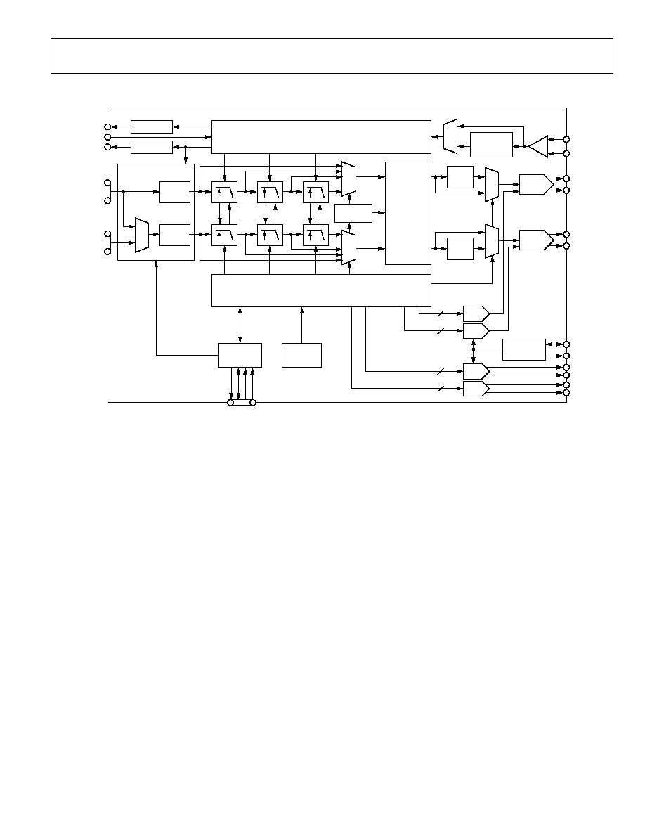
FUNCTIONAL BLOCK DIAGRAM
10
10
10
10
CLOCK GENERATION/DISTRIBUTION
DATA
ASSEMBLER
DIGITAL CONTROLLER
2
×
2
×
SYNC
1
CLOCK
MULTIPLIER
2
×
/4
×
/8
×
16-BIT
IDAC
CLK+
CLK
IOUT1_P
IOUT1_N
AUX1_P
AUX1_N
AUX2_P
AUX2_N
IOUT2_P
IOUT2_N
VREF
RSET
GAIN
GAIN
GAIN
GAIN
16-BIT
QDAC
2
×
SYNC
1
I LATCH
DELAY LINE
Q LATCH
P2D(15:0)
P1D(15:0)
SYNC_O
SYNC_I
DATACLK_OUT
2
×
2
×
2
×
n
×
f
DAC
/8
n = 1 TO 7
POWER-ON
RESET
SDO
SDIO
SCLK
CSB
REFERENCE
AND BIAS
SERIAL
PERIPHERAL
INTERFACE
COMPLEX
MODULATOR
DELAY LINE
05361-001
Figure 1.

AD9776/AD9778/AD9779
Rev. 0 | Page 4 of 56
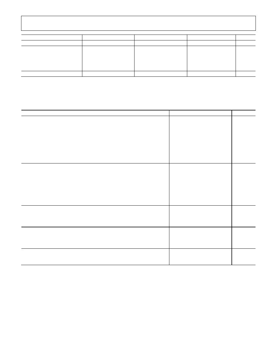
SPECIFICATIONS
T
MIN
to T
MAX
, AVDD33 = 3.3 V, DVDD33 = 3.3 V, DVDD18 = 1.8 V, CVDD18 =1.8 V, I
OUTFS
= 20 mA, maximum sample rate, unless
otherwise noted.
Table 1. AD9776, AD9778, and AD9779 DC Specifications
AD9776
AD9778
AD9779
Parameter Min
Typ
Max
Min
Typ Max Min Typ Max Unit
RESOLUTION
12
14
16
Bits
ACCURACY
Differential Nonlinearity (DNL)
±0.1
±0.65
±2.1
LSB
Integral Nonlinearity (INL)
±0.6
±1
±3.7
LSB
MAIN DAC OUTPUTS
Offset Error
0.001
0
+0.001
0.001
0
+0.001
0.001
0
+0.001
% FSR
Gain Error (with Internal
Reference)
±2
±2
±2
%
FSR
Full-Scale Output Current
1
8.66 20.2
31.66 8.66 20.2
31.66 8.66 20.2
31.66
mA
Output Compliance Range
1.0
+1.0
1.0
+1.0
1.0
+1.0
V
Output Resistance
10
10
10
M
Gain DAC Monotonicity
Guaranteed
MAIN DAC TEMPERATURE DRIFT
Offset
0.04
0.04
0.04
ppm/°C
Gain
100
100
100
ppm/°C
Reference Voltage
30
30
30
ppm/°C
AUX DAC OUTPUTS
Resolution
10
10
10
Bits
Full-Scale Output Current
1
1.998
+1.998 1.998
+1.998 1.998
+1.998
mA
Output Compliance Range
(Source)
0 1.6
0 1.6
0
1.6
V
Output Compliance Range
(Sink)
0.8 1.6 0.8 1.6 0.8 1.6 V
Output Resistance
1
1
1
M
Aux DAC Monotonicity
Guaranteed
REFERENCE
Internal Reference Voltage
1.2
1.2
1.2
V
Output Resistance
5
5
5
k
ANALOG SUPPLY VOLTAGES
AVDD33 3.13
3.3
3.47
3.13
3.3
3.47
3.13
3.3
3.47
V
CVDD18 1.70
1.8
1.90
1.70
1.8
1.90
1.70
1.8
1.90
V
DIGITAL SUPPLY VOLTAGES
DVDD33 3.13
3.3
3.47
3.13
3.3
3.47
3.13
3.3
3.47
V
DVDD18 1.70
1.8
1.90
1.70
1.8
1.90
1.70
1.8
1.90
V
POWER CONSUMPTION
1× Mode, f
DAC
= 100 MSPS,
IF = 1 MHz
250
300
250
300
250
300
mW
2× Mode, f
DAC
= 320 MSPS,
IF = 16 MHz, PLL Off
498
498
498
mW
2× Mode, f
DAC
= 320 MSPS,
IF = 16 MHz, PLL On
588
588
588
mW
4× Mode, f
DAC
/4 Mod,
f
DAC
= 500 MSPS,
IF = 137.5 MHz, Q DAC Off
572
572
572
mW
AD9776/AD9778/AD9779
Rev. 0 | Page 5 of 56
AD9776
AD9778
AD9779
Parameter Min
Typ
Max
Min
Typ Max Min Typ Max Unit
8× Mode, f
DAC
/4 Mod,
f
DAC
= 1 GSPS, IF = 262.5 MHz
980
980
980
mW
Power-Down Mode
2
3.7
2
3.7
2
3.7
mW
Power Supply Rejection Ratio--
AVDD33
0.3
+0.3 0.3
+0.3 0.3 +0.3
%
FSR/V
OPERATING RANGE
40
+25
+85
40 +25
+85 40 +25
+85
°C
1
Based on a 10 k
external resistor.
T
MIN
to T
MAX
, AVDD33 = 3.3 V, DVDD33 = 3.3 V, DVDD18 = 1.8 V, CVDD18 = 1.8 V, I
OUTFS
= 20 mA, maximum sample rate, unless
otherwise noted. LVDS driver and receiver are compliant to the IEEE-1596 reduced range link, unless otherwise noted.
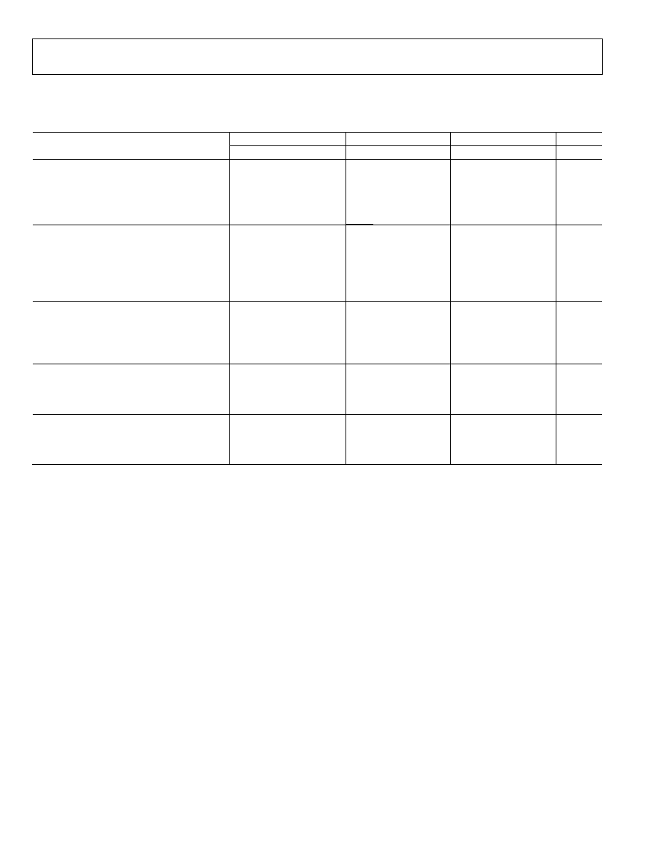
Table 2. AD9776, AD9778, and AD9779 Digital Specifications
Parameter
Min Typ Max Unit
LVDS RECEIVER INPUTS
(SYNC_I+, SYNC_I), SYNC_I+ = V
IA
, SYNC_I = V
IB
Input Voltage Range, V
IA
or V
IB
825
1575 mV
Input Differential Threshold, V
IDTH
100
+100
mV
Input Differential Hysteresis, V
IDTHH
- V
IDTHL
20
mV
Receiver Differential Input Impedance, R
IN
1
80
120
LVDS Input Rate
125
MSPS
Set-Up Time, Sync_I to DAC Clock
0.2
ns
Hold Time, Sync_I to DAC Clock
1
ns
LVDS DRIVER OUTPUTS
(SYNC_O+, SYNC_O), SYNC_O+ = V
OA
, SYNC_O = V
OB
, 100 Termination
Output Voltage High, V
OA
or V
OB
825
1575 mV
Output Voltage Low, V
OA
or V
OB
1025
mV
Output Differential Voltage, |V
OD
| 150
200
250
mV
Output Offset Voltage, V
OS
1150
1250 mV
Output Impedance, Single-Ended, R
O
80 100
120
Maximum Clock Rate
1
GHz
DAC CLOCK INPUT (CLK+, CLK)
Peak-to-Peak Voltage at CLK+ and CLK
2
400 800 1600 mV
Common-Mode Voltage
300
400
500
mV
Maximum Clock Rate
3
1
GSPS
SERIAL PERIPHERAL INTERFACE
Maximum Clock Rate (SCLK)
40
MHz
Minimum Pulse Width High
12.5
ns
Minimum Pulse Width Low
12.5
ns
INPUT DATA
Set-Up Time, Input Data To DATACLK (All Modes)
3.0
ns
Hold Time, Input Data To DATACLK (All Modes)
0.78
ns
1
Guaranteed at 25°C. Can drift above 120
at temperatures above 25°C.
2
When using the PLL, a minimum 1 V swing is recommended.
3
Typical maximum clock rate when DVDD18 = CVDD18 = 1.9 V.
AD9776/AD9778/AD9779
Rev. 0 | Page 6 of 56
T
MIN
to T
MAX
, AVDD33 = 3.3 V, DVDD33 = 3.3 V, DVDD18 = 1.8 V, CVDD18 = 1.8 V, I
OUTFS
= 20 mA, maximum sample rate, unless
otherwise noted.
Table 3. AD9776, AD9778, and AD9779 AC Specifications
AD9776
AD9778
AD9779
Parameter Min
Typ
Max
Min
Typ Max
Min
Typ Max
Unit
SPURIOUS FREE DYNAMIC RANGE (SFDR)
f
DAC
= 100 MSPS, f
OUT
= 20 MHz
82
82
82
dBc
f
DAC
= 200 MSPS, f
OUT
= 50 MHz
81
81
82
dBc
f
DAC
= 400 MSPS, f
OUT
= 70 MHz
80
80
80
dBc
f
DAC
= 800 MSPS, f
OUT
= 70 MHz
85
85
87
dBc
TWO-TONE INTERMODULATION DISTORTION
(IMD)
f
DAC
= 200 MSPS, f
OUT
= 50 MHz
87
87
91
dBc
f
DAC
= 400 MSPS, f
OUT
= 60 MHz
80
85
85
dBc
f
DAC
= 400 MSPS, f
OUT
= 80 MHz
75
81
81
dBc
f
DAC
= 800 MSPS, f
OUT
= 100 MHz
75
80
81
dBc
NOISE SPECTRAL DENSITY (NSD) Eight-Tone,
500 kHz Tone Spacing
f
DAC
= 200 MSPS, f
OUT
= 80 MHz
152
155
158
dBm/Hz
f
DAC
= 400 MSPS, f
OUT
= 80 MHz
155
159
160
dBm/Hz
f
DAC
= 800 MSPS, f
OUT
= 80 MHz
157.5
160
161
dBm/Hz
WCDMA ADJACENT CHANNEL LEAKAGE
RATIO (ACLR), SINGLE CARRIER
f
DAC
= 491.52 MSPS, f
OUT
= 100 MHz
76
78
79
dBc
f
DAC
= 491.52 MSPS, f
OUT
= 200 MHz
69
73
74
dBc
WCDMA SECOND ADJACENT CHANNEL
LEAKAGE RATIO (ACLR), SINGLE CARRIER
f
DAC
= 491.52 MSPS, f
OUT
= 100 MHz
77.5
80
81
dBc
f
DAC
= 491.52 MSPS, f
OUT
= 200 MHz
76
78
78
dBc
AD9776/AD9778/AD9779
Rev. 0 | Page 7 of 56
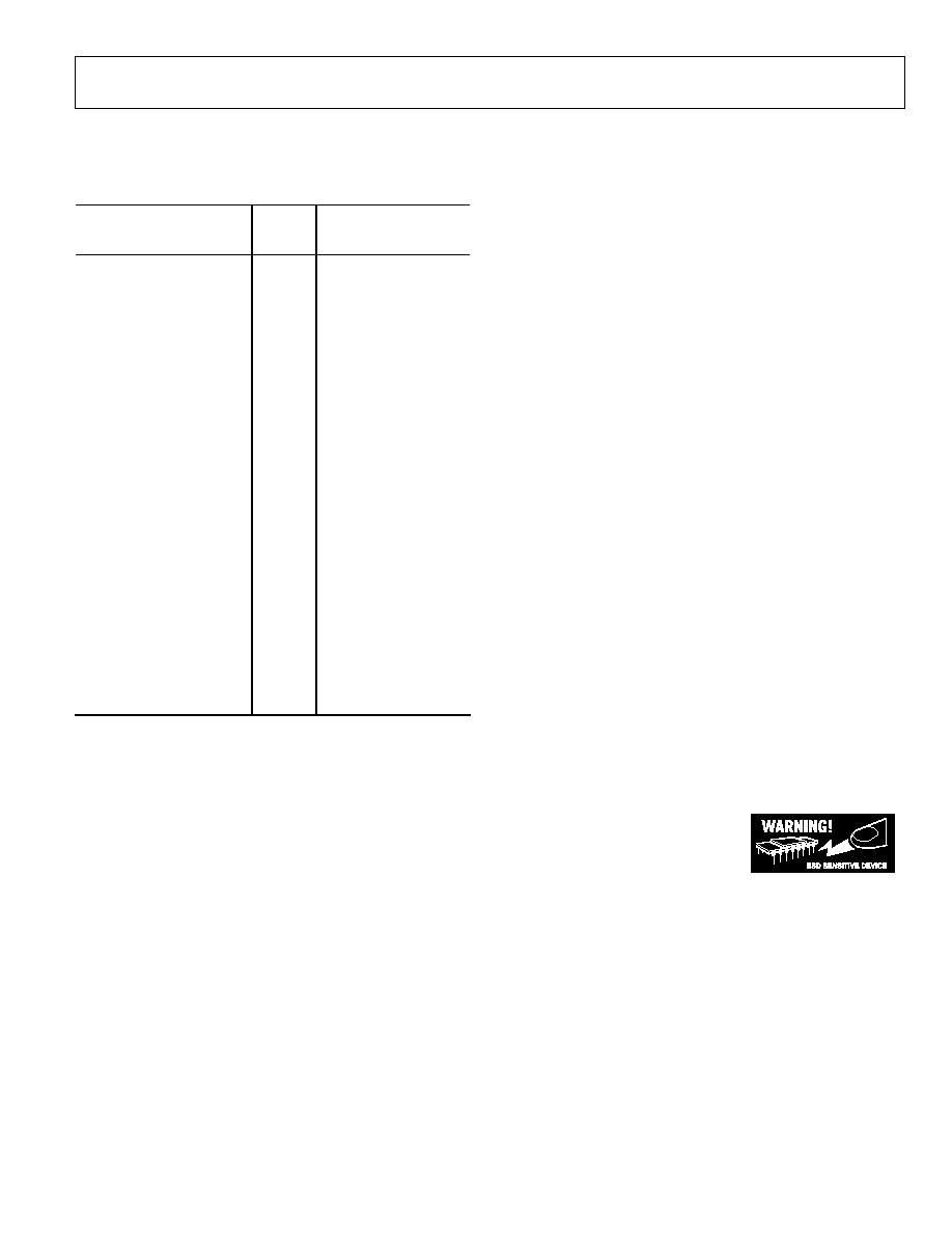
ABSOLUTE MAXIMUM RATINGS
Table 4.
Parameter
With
Respect
to Rating
AVDD33 AGND
DGND
CGND
-0.3 V to +3.6 V
DVDD33, DVDD18, CVDD18
AGND
DGND
CGND
-0.3 V to +1.98 V
AGND DGND
CGND
-0.3 V to +0.3 V
DGND AGND
CGND
-0.3 V to +0.3 V
CGND AGND
DGND
-0.3 V to +0.3 V
I120, VREF, IPTAT
AGND
-0.3 V to AVDD33 + 0.3 V
I
OUT1-P
, I
OUT1-N
, I
OUT2-P
,
I
OUT2-N
, Aux
1-P
, Aux
1-N
, Aux
2-P
,
Aux
2-N
AGND
-1.0 V to AVDD33 + 0.3 V
P1D15 to P1D0,
P2D15 to P2D0
DGND
-0.3 V to DVDD33 + 0.3 V
DATACLK, TXENABLE
DGND
-0.3 V to DVDD33 + 0.3 V
CLK+, CLK-, RESET, IRQ,
PLL_LOCK, SYNC_O+,
SYNC_O-, SYNC_I+, SYNC_I
CGND
-0.3 V to CVDD18 + 0.3 V
RESET, IRQ, PLL_LOCK,
SYNC_O+, SYNC_O,
SYNC_I+, SYNC_I, CSB,
SCLK, SDIO, SDO
DGND
0.3 V to DVDD33 + 0.3 V
Junction Temperature
+125°C
Storage Temperature
-65°C to +150°C
Thermal Resistance
100-lead, thermally enhanced TQFP Package
JA
= 27.4°C/W
(with no airflow movement).
Stresses above those listed under Absolute Maximum Ratings
may cause permanent damage to the device. This is a stress
rating only and functional operation of the device at these or
any other conditions above those indicated in the operational
section of this specification is not implied. Exposure to absolute
maximum rating conditions for extended periods may affect
device reliability.
ESD CAUTION
ESD (electrostatic discharge) sensitive device. Electrostatic charges as high as 4000 V readily accumulate on
the human body and test equipment and can discharge without detection. Although this product features
proprietary ESD protection circuitry, permanent damage may occur on devices subjected to high energy
electrostatic discharges. Therefore, proper ESD precautions are recommended to avoid performance
degradation or loss of functionality.
AD9776/AD9778/AD9779
Rev. 0 | Page 8 of 56
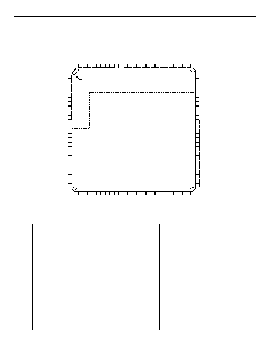
PIN CONFIGURATIONS AND FUNCTION DESCRIPTIONS
74
VREF
73
IPTAT
72
AGND
69
CSB
70
RESET
71
IRQ
75
I120
68
SCLK
67
SDIO
66
SDO
64
DGND
63
SYNC_O+
62
SYNC_O
61
DVDD33
60
DVDD18
59
NC
58
NC
57
NC
56
NC
55
P2D<0>
54
DGND
53
DVDD18
52
P2D<1>
51
P2D<2>
65
PLL_LOCK
PIN 1
100
AV
DD3
3
99
AGND
98
AV
DD3
3
97
AGND
96
AV
DD3
3
95
AGND
94
AGND
93
OU
T1_P
92
OU
T1_N
91
AGND
90
AUX
1
_
P
89
AUX
1
_
N
88
AGND
87
AUX
2
_
N
86
AUX
2
_
P
85
AGND
84
OU
T2_N
83
OU
T2_P
82
AGND
81
AGND
80
AV
DD3
3
79
AGND
78
AV
DD3
3
77
AGND
76
AV
DD3
3
26
P1D
<
4>
27
P1D
<
3>
28
P1D
<
2>
29
P1D
<
1>
30
P1D
<
0>
31
NC
32
DGND
33
DV
DD1
8
34
NC
35
NC
36
NC
37
DATACLK
38
DV
DD3
3
39
TX
E
NABLE
40
P2D
<
11>
41
P2D
<
10>
42
P2D
<
9>
43
DV
DD1
8
44
DGND
45
P2D
<
8>
46
P2D
<
7>
47
P2D
<
6>
48
P2D
<
5>
49
P2D
<
4>
50
P2D
<
3>
2
CVDD18
3
CGND
4
CGND
7
CGND
6
CLK
5
CLK+
1
CVDD18
8
CGND
9
CVDD18
10
CVDD18
12
AGND
13
SYNC_I+
14
SYNC_I
15
DGND
16
DVDD18
17
P1D<11>
18
P1D<10>
19
P1D<9>
20
P1D<8>
21
P1D<7>
22
DGND
23
DVDD18
24
P1D<6>
25
P1D<5>
11
CGND
AD9776
TOP VIEW
(Not to Scale)
ANALOG DOMAIN
DIGITAL DOMAIN
NC = NO CONNECT
05361-004
Figure 2. AD9776 Pin Configuration
Table 5. AD 9776 Pin Function Description
Pin No.
Mnemonic
Description
1
CVDD18
1.8 V Clock Supply
2
CVDD18
1.8 V Clock Supply
3 CGND Clock
Common
4 CGND Clock
Common
5 CLK+
1
Differential Clock Input
6 CLK
1
Differential Clock Input
7 CGND Clock
Common
8 CGND Clock
Common
9
CVDD18
1.8 V Clock Supply
10
CVDD18
1.8 V Clock Supply
11 CGND
Clock
Common
12 AGND
Analog
Common
13
SYNC_I+
Differential Synchronization Input
14
SYNC_I
Differential Synchronization Input
15 DGND
Digital
Common
16
DVDD18
1.8 V Digital Supply
17
P1D <11>
Port 1, Data Input D11 (MSB)
18
P1D <10>
Port 1, Data Input D10
Pin No.
Mnemonic
Description
19
P1D <9>
Port 1, Data Input D9
20
P1D <8>
Port 1, Data Input D8
21
P1D <7>
Port 1, Data Input D7
22 DGND
Digital
Common
23
DVDD18
1.8 V Digital Supply
24
P1D <6>
Port 1, Data Input D6
25
P1D <5>
Port 1, Data Input D5
26
P1D <4>
Port 1, Data Input D4
27
P1D <3>
Port 1, Data Input D3
28
P1D <2>
Port 1, Data Input D2
29
P1D <1>
Port 1, Data Input D1
30
P1D <0>
Port 1, Data Input D0
31 NC
No
Connect
32 DGND
Digital
Common
33
DVDD18
1.8 V Digital Supply
34 NC
No
Connect
35 NC
No
Connect
36 NC
No
Connect

AD9776/AD9778/AD9779
Rev. 0 | Page 9 of 56
Pin No.
Mnemonic
Description
37
DATACLK
Data Clock Output
38
DVDD33
3.3 V Digital Supply
39 TXENABLE
Transmit
Enable
40
P2D <11>
Port 2, Data Input D11 (MSB)
41
P2D <10>
Port 2, Data Input D10
42
P2D <9>
Port 2, Data Input D9
43
DVDD18
1.8 V Digital Supply
44 DGND
Digital
Common
45
P2D <8>
Port 2, Data Input D8
46
P2D <7>
Port 2, Data Input D7
47
P2D <6>
Port 2, Data Input D6
48
P2D <5>
Port 2, Data Input D5
49
P2D <4>
Port 2, Data Input D4
50
P2D <3>
Port 2, Data Input D3
51
P2D <2>
Port 2, Data Input D2
52
P2D <1>
Port 2, Data Input D1
53
DVDD18
1.8 V Digital Supply
54 DGND
Digital
Common
55
P2D <0>
Port 2, Data Input D0
56 NC
No
Connect
57 NC
No
Connect
58 NC
No
Connect
59 NC
No
Connect
60
DVDD18
1.8 V Digital Supply
61
DVDD33
3.3 V Digital Supply
62
SYNC_O
Differential Synchronization Output
63
SYNC_O+
Differential Synchronization Output
64 DGND
Digital
Common
65
PLL_LOCK
PLL Lock Indicator
66
SDO
SPI Port Data Output
67
SDIO
SPI Port Data Input/Output
68
SCLK
SPI Port Clock
69
CSB
SPI Port Chip Select Bar
70
RESET
Reset, Active High
71 IRQ
Interrupt
Request
72 AGND
Analog
Common
73 IPTAT
Reference
Current
Pin No.
Mnemonic
Description
74
VREF
Voltage Reference Output
75
I120
120 A Reference Current
76
AVDD33
3.3 V Analog Supply
77 AGND
Analog
Common
78
AVDD33
3.3 V Analog Supply
79 AGND
Analog
Common
80
AVDD33
3.3 V Analog Supply
81 AGND
Analog
Common
82 AGND
Analog
Common
83 OUT2_P Differential DAC Current Output,
Channel 2
84 OUT2_N Differential DAC Current Output,
Channel 2
85 AGND
Analog
Common
86 AUX2_P Auxiliary DAC Voltage Output,
Channel 2
87 AUX2_N Auxiliary DAC Voltage Output,
Channel 2
88 AGND
Analog
Common
89 AUX1_N Auxiliary DAC Voltage Output,
Channel 1
90 AUX1_P Auxiliary DAC Voltage Output,
Channel 1
91 AGND
Analog
Common
92 OUT1_N Differential DAC Current Output,
Channel 1
93 OUT1_P Differential DAC Current Output,
Channel 1
94 AGND
Analog
Common
95 AGND
Analog
Common
96
AVDD33
3.3 V Analog Supply
97 AGND
Analog
Common
98
AVDD33
3.3 V Analog Supply
99 AGND
Analog
Common
100
AVDD33
3.3 V Analog Supply
1
The combined differential clock input at the CLK+ and CLK pins are referred
to as DACCLK.
AD9776/AD9778/AD9779
Rev. 0 | Page 10 of 56
74
VREF
73
IPTAT
72
AGND
69
CSB
70
RESET
71
IRQ
75
I120
68
SCLK
67
SDIO
66
SDO
64
DGND
63
SYNC_O+
62
SYNC_O
61
DVDD33
60
DVDD18
59
NC
58
NC
57
P2D<0>
56
P2D<1>
55
P2D<2>
54
DGND
53
DVDD18
52
P2D<3>
51
P2D<4>
65
PLL_LOCK
PIN 1
100
AV
DD3
3
99
AGND
98
AV
DD3
3
97
AGND
96
AV
DD3
3
95
AGND
94
AGND
93
OU
T1_P
92
OU
T1_N
91
AGND
90
A
U
X1_P
89
A
U
X1_N
88
AGND
87
A
U
X2_N
86
A
U
X2_P
85
AGND
84
OU
T2_N
83
OU
T2_P
82
AGND
81
AGND
80
AV
DD3
3
79
AGND
78
AV
DD3
3
77
AGND
76
AV
DD3
3
26
P1D
<
6>
27
P1D
<
5>
28
P1D
<
4>
29
P1D
<
3>
30
P1D
<
2>
31
P1D
<
1>
32
DGND
33
DV
DD1
8
34
P1D
<
0>
35
NC
36
NC
37
DATACLK
38
DV
DD3
3
39
TX
E
NABLE
40
P2D
<
13>
41
P2D
<
12>
42
P2D
<
11>
43
DV
DD1
8
44
DGND
45
P2D
<
10>
46
P2D
<
9>
47
P2D
<
8>
48
P2D
<
7>
49
P2D
<
6>
50
P2D
<
5>
2
CVDD18
3
CGND
4
CGND
7
CGND
6
CLK
5
CLK+
1
CVDD18
8
CGND
9
CVDD18
10
CVDD18
12
AGND
13
SYNC_I+
14
SYNC_I
15
DGND
16
DVDD18
17
P1D<13>
18
P1D<12>
19
P1D<11>
20
P1D<10>
21
P1D<9>
22
DGND
23
DVDD18
24
P1D<8>
25
P1D<7>
11
CGND
AD9778
TOP VIEW
(Not to Scale)
ANALOG DOMAIN
DIGITAL DOMAIN
NC = NO CONNECT
05361-003
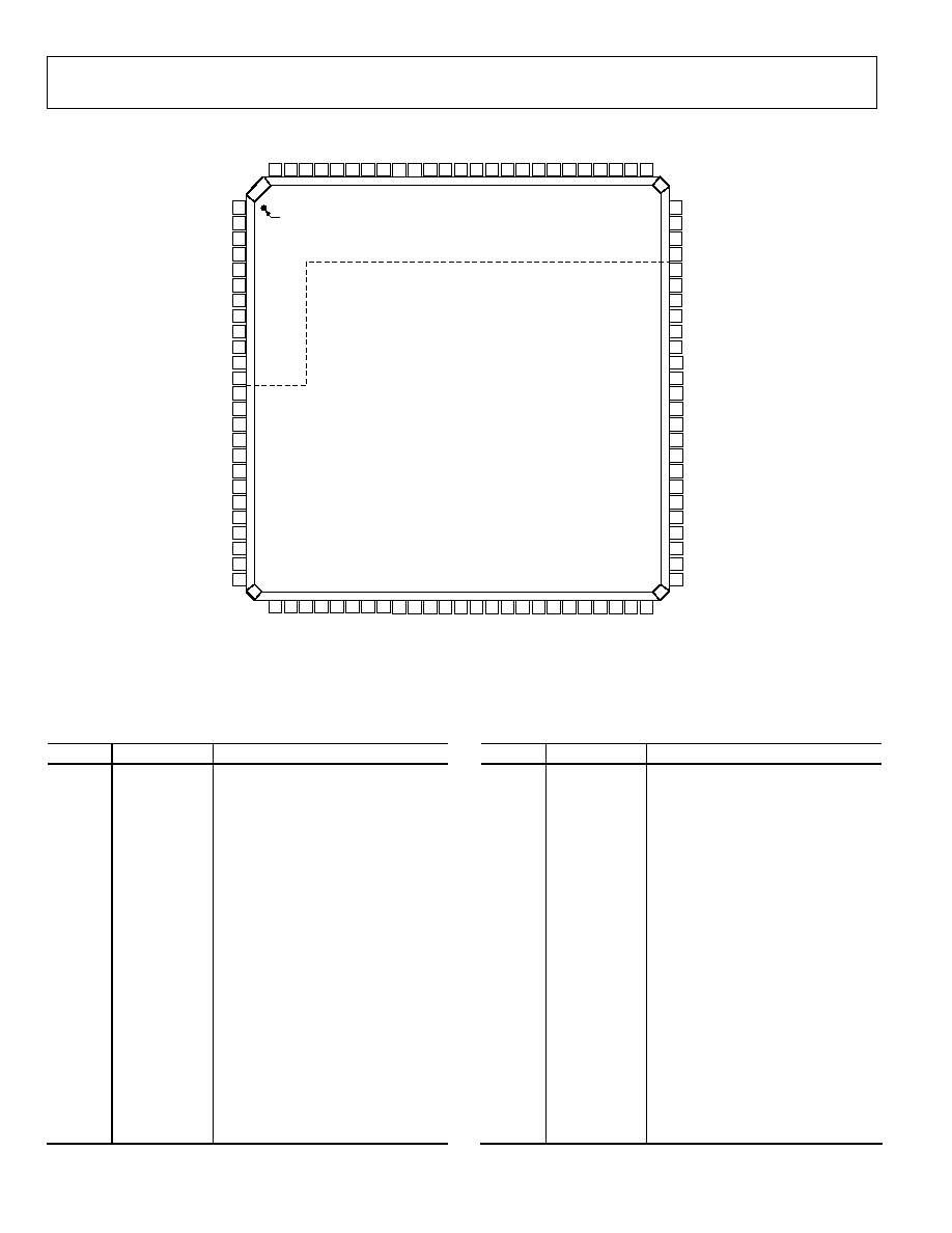
Figure 3. AD9778 Pin Configuration
Table 6. AD 9778 Pin Function Description
Pin No.
Mnemonic
Description
1
CVDD18
1.8 V Clock Supply
2
CVDD18
1.8 V Clock Supply
3 CGND Clock
Common
4 CGND Clock
Common
5 CLK+
1
Differential Clock Input
6 CLK
1
Differential Clock Input
7 CGND Clock
Common
8 CGND Clock
Common
9
CVDD18
1.8 V Clock Supply
10
CVDD18
1.8 V Clock Supply
11 CGND
Clock
Common
12 AGND
Analog
Common
13
SYNC_I+
Differential Synchronization Input
14
SYNC_I
Differential Synchronization Input
15 DGND
Digital
Common
16
DVDD18
1.8 V Digital Supply
17
P1D <13>
Port 1, Data Input D13 (MSB)
18
P1D <12>
Port 1, Data Input D12
19
P1D <11>
Port 1, Data Input D11
20
P1D <10>
Port 1, Data Input D10
Pin No.
Mnemonic
Description
21
P1D <9>
Port 1, Data Input D9
22 DGND
Digital
Common
23
DVDD18
1.8 V Digital Supply
24
P1D <8>
Port 1, Data Input D8
25
P1D <7>
Port 1, Data Input D7
26
P1D <6>
Port 1, Data Input D6
27
P1D <5>
Port 1, Data Input D5
28
P1D <4>
Port 1, Data Input D4
29
P1D <3>
Port 1, Data Input D3
30
P1D <2>
Port 1, Data Input D2
31
P1D <1>
Port 1, Data Input D1
32 DGND
Digital
Common
33
DVDD18
1.8 V Digital Supply
34
P1D <0>
Port 1, Data Input D0
35 NC
No
Connect
36 NC
No
Connect
37
DATACLK
Data Clock Output
38
DVDD33
3.3 V Digital Supply
39 TXENABLE
Transmit
Enable
40
P2D <13>
Port 2, Data Input D13 (MSB)

AD9776/AD9778/AD9779
Rev. 0 | Page 11 of 56
Pin No.
Mnemonic
Description
41
P2D <12>
Port 2, Data Input D12
42
P2D <11>
Port 2, Data Input D11
43
DVDD18
1.8 V Digital Supply
44 DGND
Digital
Common
45
P2D <10>
Port 2, Data Input D10
46
P2D <9>
Port 2, Data Input D9
47
P2D <8>
Port 2, Data Input D8
48
P2D <7>
Port 2, Data Input D7
49
P2D <6>
Port 2, Data Input D6
50
P2D <5>
Port 2, Data Input D5
51
P2D <4>
Port 2, Data Input D4
52
P2D <3>
Port 2, Data Input D3
53
DVDD18
1.8 V Digital Supply
54 DGND
Digital
Common
55
P2D <2>
Port 2, Data Input D2
56
P2D <1>
Port 2, Data Input D1
57
P2D <0>
Port 2, Data Input D0
58 NC
No
Connect
59 NC
No
Connect
60
DVDD18
1.8 V Digital Supply
61
DVDD33
3.3 V Digital Supply
62
SYNC_O
Differential Synchronization Output
63
SYNC_O+
Differential Synchronization Output
64 DGND
Digital
Common
65
PLL_LOCK
PLL Lock Indicator
66
SDO
SPI Port Data Output
67
SDIO
SPI Port Data Input/Output
68
SCLK
SPI Port Clock
69
CSB
SPI Port Chip Select Bar
70
RESET
Reset, Active High
71 IRQ
Interrupt
Request
72 AGND
Analog
Common
73 IPTAT
Reference
Current
74
VREF
Voltage Reference Output
75
I120
120 A Reference Current
Pin No.
Mnemonic
Description
76
AVDD33
3.3 V Analog Supply
77 AGND
Analog
Common
78
AVDD33
3.3 V Analog Supply
79 AGND
Analog
Common
80
AVDD33
3.3 V Analog Supply
81 AGND
Analog
Common
82 AGND
Analog
Common
83 OUT2_P Differential DAC Current Output,
Channel 2
84 OUT2_N Differential DAC Current Output,
Channel 2
85 AGND
Analog
Common
86 AUX2_P Auxiliary DAC Voltage Output,
Channel 2
87 AUX2_N Auxiliary DAC Voltage Output,
Channel 2
88 AGND
Analog
Common
89 AUX1_N Auxiliary DAC Voltage Output,
Channel 1
90 AUX1_P Auxiliary DAC Voltage Output,
Channel 1
91 AGND
Analog
Common
92 OUT1_N Differential DAC Current Output,
Channel 1
93 OUT1_P Differential DAC Current Output,
Channel 1
94 AGND
Analog
Common
95 AGND
Analog
Common
96
AVDD33
3.3 V Analog Supply
97 AGND
Analog
Common
98
AVDD33
3.3 V Analog Supply
99 AGND
Analog
Common
100
AVDD33
3.3 V Analog Supply
1
The combined differential clock input at the CLK+ and CLK pins are referred
to as DACCLK.

AD9776/AD9778/AD9779
Rev. 0 | Page 12 of 56
74
VREF
73
IPTAT
72
AGND
69
CSB
70
RESET
71
IRQ
75
I120
68
SCLK
67
SDIO
66
SDO
64
DGND
63
SYNC_O+
62
SYNC_O
61
DVDD33
60
DVDD18
59
NC
58
NC
57
NC
56
NC
55
P2D<0>
54
DGND
53
DVDD18
52
P2D<1>
51
P2D<2>
65
PLL_LOCK
PIN 1
100
AV
DD3
3
99
AGND
98
AV
DD3
3
97
AGND
96
AV
DD3
3
95
AGND
94
AGND
93
OU
T1_P
92
OU
T1_N
91
AGND
90
A
U
X1_P
89
A
U
X1_N
88
AGND
87
A
U
X2_N
86
A
U
X2_P
85
AGND
84
OU
T2_N
83
OU
T2_P
82
AGND
81
AGND
80
AV
DD3
3
79
AGND
78
AV
DD3
3
77
AGND
76
AV
DD3
3
26
P1D
<
4>
27
P1D
<
3>
28
P1D
<
2>
29
P1D
<
1>
30
P1D
<
0>
31
NC
32
DGND
33
DV
DD1
8
34
NC
35
NC
36
NC
37
DATACLK
38
DV
DD3
3
39
TX
E
NABLE
40
P2D
<
11>
41
P2D
<
10>
42
P2D
<
9>
43
DV
DD1
8
44
DGND
45
P2D
<
8>
46
P2D
<
7>
47
P2D
<
6>
48
P2D
<
5>
49
P2D
<
4>
50
P2D
<
3>
2
CVDD18
3
CGND
4
CGND
7
CGND
6
CLK
5
CLK+
1
CVDD18
8
CGND
9
CVDD18
10
CVDD18
12
AGND
13
SYNC_I+
14
SYNC_I
15
DGND
16
DVDD18
17
P1D<11>
18
P1D<10>
19
P1D<9>
20
P1D<8>
21
P1D<7>
22
DGND
23
DVDD18
24
P1D<6>
25
P1D<5>
11
CGND
AD9776
TOP VIEW
(Not to Scale)
ANALOG DOMAIN
DIGITAL DOMAIN
NC = NO CONNECT
05361-004
Figure 4. AD9779 Pin Configuration
Table 7. AD9779 Pin Function Descriptions
Pin No.
Mnemonic
Description
1
CVDD18
1.8 V Clock Supply
2
CVDD18
1.8 V Clock Supply
3 CGND Clock
Common
4 CGND Clock
Common
5 CLK+
1
Differential Clock Input
6 CLK
1
Differential Clock Input
7 CGND Clock
Common
8 CGND Clock
Common
9
CVDD18
1.8 V Clock Supply
10
CVDD18
1.8 V Clock Supply
11 CGND
Clock
Common
12 AGND
Analog
Common
13
SYNC_I+
Differential Synchronization Input
14
SYNC_I
Differential Synchronization Input
15 DGND
Digital
Common
16
DVDD18
1.8 V Digital Supply
17
P1D <15>
Port 1, Data Input D15 (MSB)
18
P1D <14>
Port 1, Data Input D14
19
P1D <13>
Port 1, Data Input D13
Pin No.
Mnemonic
Description
20
P1D <12>
Port 1, Data Input D12
21
P1D <11>
Port 1, Data Input D11
22 DGND
Digital
Common
23
DVDD18
1.8 V Digital Supply
24
P1D <10>
Port 1, Data Input D10
25
P1D <9>
Port 1, Data Input D9
26
P1D <8>
Port 1, Data Input D8
27
P1D <7>
Port 1, Data Input D7
28
P1D <6>
Port 1, Data Input D6
29
P1D <5>
Port 1, Data Input D5
30
P1D <4>
Port 1, Data Input D4
31
P1D <3>
Port 1, Data Input D3
32 DGND
Digital
Common
33
DVDD18
1.8 V Digital Supply
34
P1D <2>
Port 1, Data Input D2
35
P1D <1>
Port 1, Data Input D1
36
P1D <0>
Port 1, Data Input D0 (LSB)
37
DATACLK
Data Clock Output
38
DVDD33
3.3 V Digital Supply

AD9776/AD9778/AD9779
Rev. 0 | Page 13 of 56
Pin No.
Mnemonic
Description
39 TXENABLE
Transmit
Enable
40
P2D <15>
Port 2, Data Input D15 (MSB)
41
P2D <14>
Port 2, Data Input D14
42
P2D <13>
Port 2, Data Input D13
43
DVDD18
1.8 V Digital Supply
44 DGND
Digital
Common
45
P2D <12>
Port 2, Data Input D12
46
P2D <11>
Port 2, Data Input D11
47
P2D <10>
Port 2, Data Input D10
48
P2D <9>
Port 2, Data Input D9
49
P2D <8>
Port 2, Data Input D8
50
P2D <7>
Port 2, Data Input D7
51
P2D <6>
Port 2, Data Input D6
52
P2D <5>
Port 2, Data Input D5
53
DVDD18
1.8 V Digital Supply
54 DGND
Digital
Common
55
P2D <4>
Port 2, Data Input D4
56
P2D <3>
Port 2, Data Input D3
57
P2D <2>
Port 2, Data Input D2
58
P2D <1>
Port 2, Data Input D1
59
P2D <0>
Port 2, Data Input D0 (LSB)
60
DVDD18
1.8 V Digital Supply
61
DVDD33
3.3 V Digital Supply
62
SYNC_O
Differential Synchronization Output
63
SYNC_O+
Differential Synchronization Output
64 DGND
Digital
Common
65
PLL_LOCK
PLL Lock Indicator
66
SPI_SDO
SPI Port Data Output
67 SPI_SDIO SPI
Port Data Input/Output
68
SCLK
SPI Port Clock
69
SPI_CSB
SPI Port Chip Select Bar
70
RESET
Reset, Active High
71 IRQ
Interrupt
Request
72 AGND
Analog
Common
73 IPTAT
Reference
Current
74
VREF
Voltage Reference Output
Pin No.
Mnemonic
Description
75
I120
120 A Reference Current
76
AVDD33
3.3 V Analog Supply
77 AGND
Analog
Common
78
AVDD33
3.3 V Analog Supply
79 AGND
Analog
Common
80
AVDD33
3.3 V Analog Supply
81 AGND
Analog
Common
82 AGND
Analog
Common
83 OUT2_P Differential DAC Current Output,
Channel 2
84 OUT2_N Differential DAC Current Output,
Channel 2
85 AGND
Analog
Common
86 AUX2_P Auxiliary DAC Voltage Output,
Channel 2
87 AUX2_N Auxiliary DAC Voltage Output,
Channel 2
88 AGND
Analog
Common
89 AUX1_N Auxiliary DAC Voltage Output,
Channel 1
90 AUX1_P Auxiliary DAC Voltage Output,
Channel 1
91 AGND
Analog
Common
92 OUT1_N Differential DAC Current Output,
Channel 1
93 OUT1_P Differential DAC Current Output,
Channel 1
94 AGND
Analog
Common
95 AGND
Analog
Common
96
AVDD33
3.3 V Analog Supply
97 AGND
Analog
Common
98
AVDD33
3.3 V Analog Supply
99 AGND
Analog
Common
100
AVDD33
3.3 V Analog Supply
1
The combined differential clock input at the CLK+ and CLK pins are referred
to as DACCLK.

AD9776/AD9778/AD9779
Rev. 0 | Page 14 of 56
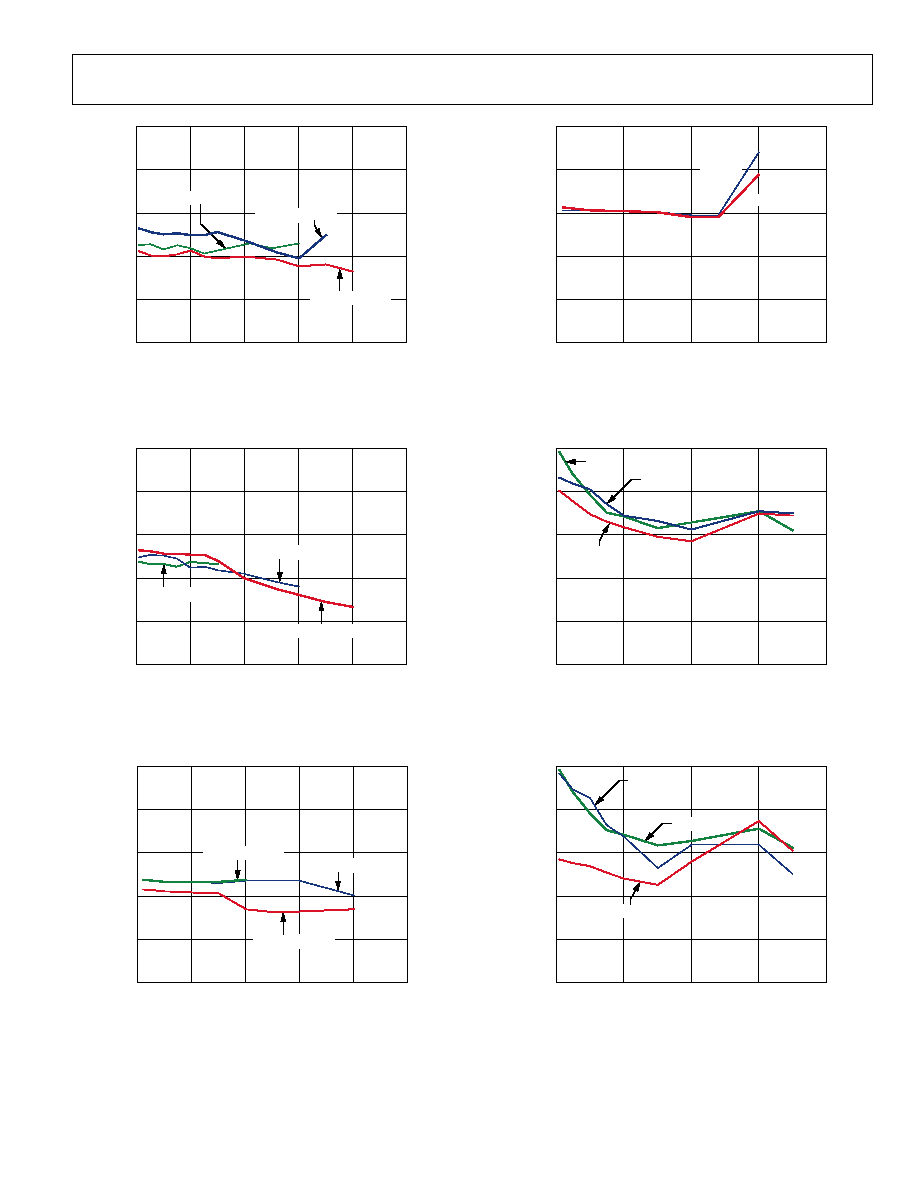
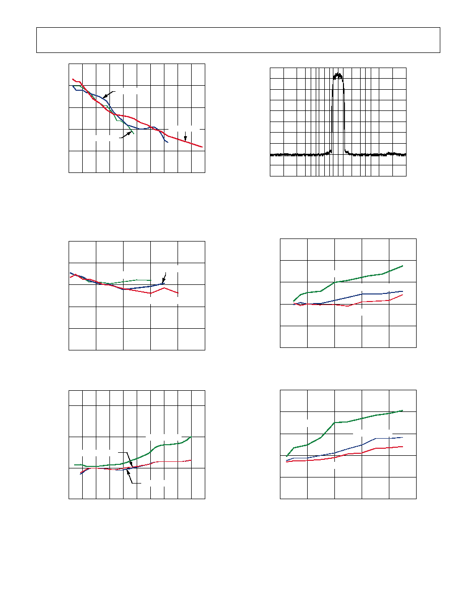
TYPICAL PERFORMANCE CHARACTERISTICS
4.0
6.0
0
80k
CODE
INL (16-BIT LSB)
3.0
2.0
1.0
0
1.0
2.0
3.0
4.0
5.0
10k
20k
30k
40k
50k
60k
70k
05361-005
Figure 5. AD9779 Typical INL
1.0
2.0
0
80k
CODE
DNL (1
6
-
BI
T LS
B)
10k
20k
30k
40k
50k
60k
70k
0.5
0
0.5
1.0
1.5
05361-006
Figure 6. AD9779 Typical DNL
100
50
0
100
f
OUT
(MHz)
S
F
DR (dBc
)
90
80
70
60
20
40
60
80
f
DATA
= 160MSPS
f
DATA
= 200MSPS
f
DATA
= 250MSPS
05361-007
Figure 7. AD9779 In-Band SFDR vs. f
OUT
, 1x Interpolation
100
50
0
100
f
OUT
(MHz)
S
F
DR (dBc
)
90
80
70
60
20
40
60
80
f
DATA
= 160MSPS
f
DATA
= 200MSPS
f
DATA
= 250MSPS
05361-008
Figure 8. AD9779 In-Band SFDR vs. f
OUT
, 2× Interpolation
100
50
0
100
f
OUT
(MHz)
S
F
DR (dBc
)
90
80
70
60
20
40
60
80
f
DATA
= 100MSPS
f
DATA
= 200MSPS
f
DATA
= 150MSPS
05361-009
Figure 9. AD9779 In-Band SFDR vs. f
OUT
, 4× Interpolation
100
50
0
50
f
OUT
(MHz)
S
F
DR (dBc
)
90
80
70
60
10
20
30
40
f
DATA
= 50MSPS
f
DATA
= 100MSPS
f
DATA
= 125MSPS
05361-010
Figure 10. AD9779 In-Band SFDR vs. f
OUT
, 8× Interpolation
AD9776/AD9778/AD9779
Rev. 0 | Page 15 of 56
100
50
0
100
f
OUT
(MHz)
S
F
DR (dBc
)
90
80
70
60
20
40
60
80
f
DATA
= 200MSPS
f
DATA
= 160MSPS
f
DATA
= 250MSPS
05361-011
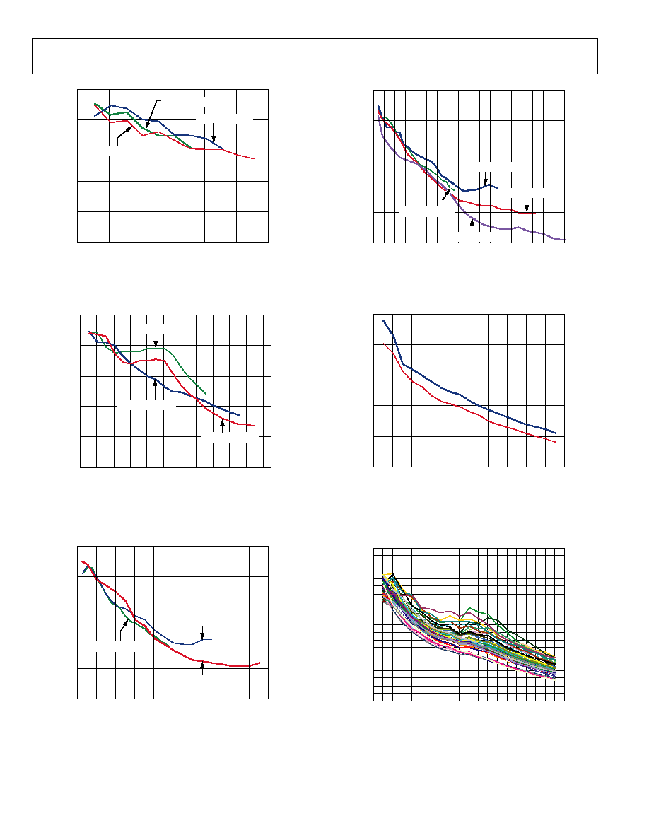
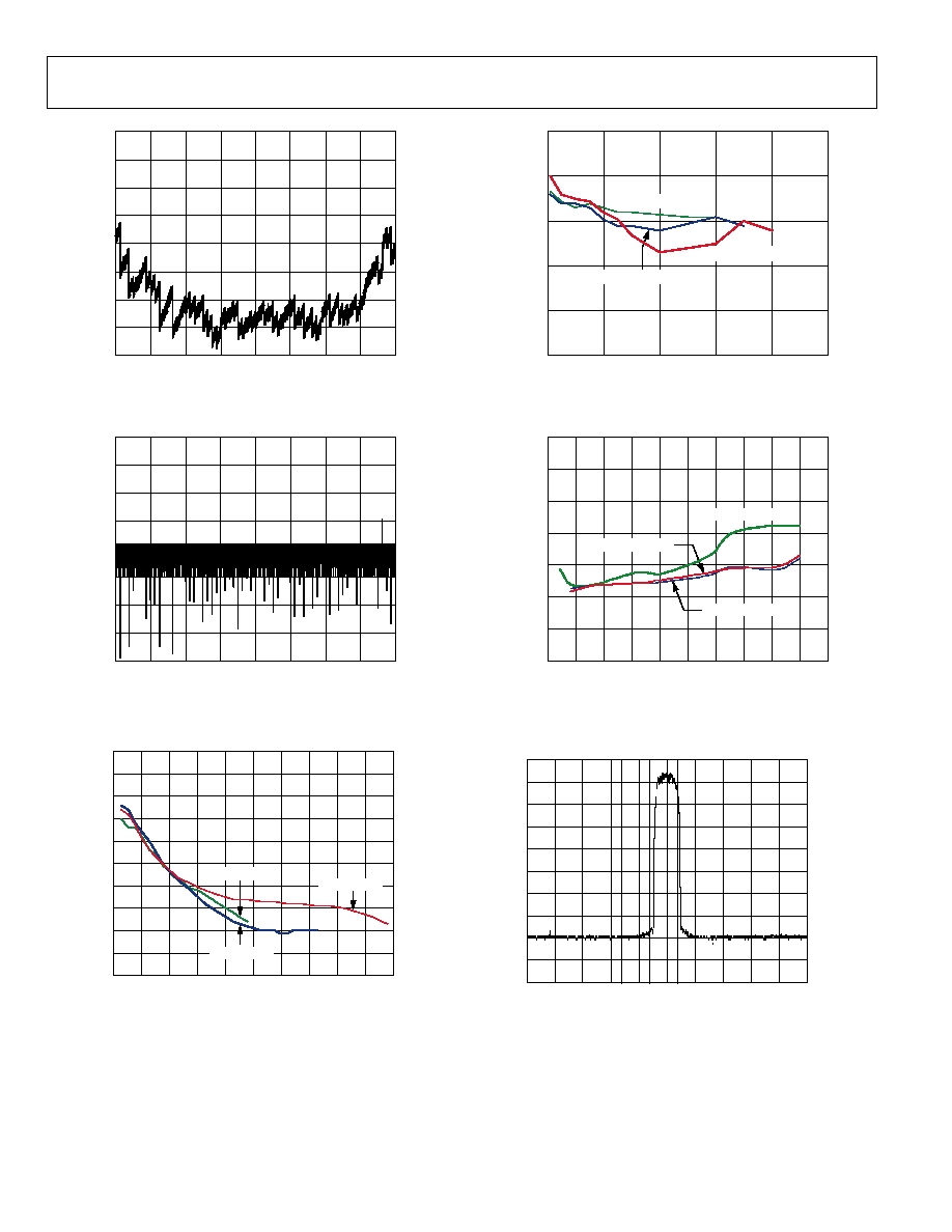
Figure 11. AD9779 Out-of-Band SFDR vs. f
OUT
, 2× Interpolation
100
50
0
100
f
OUT
(MHz)
S
F
DR (dBc
)
90
80
70
60
20
40
60
80
f
DATA
= 150MSPS
f
DATA
= 100MSPS
f
DATA
= 200MSPS
05361-012
Figure 12. AD9779 Out-of-Band SFDR vs. f
OUT
, 4× Interpolation
100
50
0
50
f
OUT
(MHz)
S
F
DR (dBc
)
90
80
70
60
10
20
30
40
f
DATA
= 50MSPS
f
DATA
= 100MSPS
f
DATA
= 125MSPS
05361-013
Figure 13. AD9779 Out-of-Band SFDR vs. f
OUT
, 8× Interpolation
100
50
0
40
f
OUT
(MHz)
S
F
DR (dBc
)
90
80
70
60
10
20
30
PLL OFF
PLL ON
05361-014
Figure 14. AD9779 In-Band SFDR, 4× Interpolation,
f
DATA
= 100 MSPS, PLL On/Off
100
50
0
80
f
OUT
(MHz)
S
F
DR (dBc
)
90
80
70
60
20
40
60
3dBFS
0dBFS
6dBFS
05361-015
Figure 15. AD9779 In-Band SFDR vs. Digital Full-Scale Input
100
50
0
80
f
OUT
(MHz)
S
F
DR (dBc
)
90
80
70
60
20
40
60
10mA
20mA
30mA
05361-016
Figure 16. AD9779 In-Band SFDR vs. Output Full-Scale Current
AD9776/AD9778/AD9779
Rev. 0 | Page 16 of 56
100
50
0
120
f
OUT
(MHz)
IMD (dBc
)
90
80
70
60
20
40
60
80
100
f
DATA
= 200MSPS
f
DATA
= 250MSPS
f
DATA
= 160MSPS
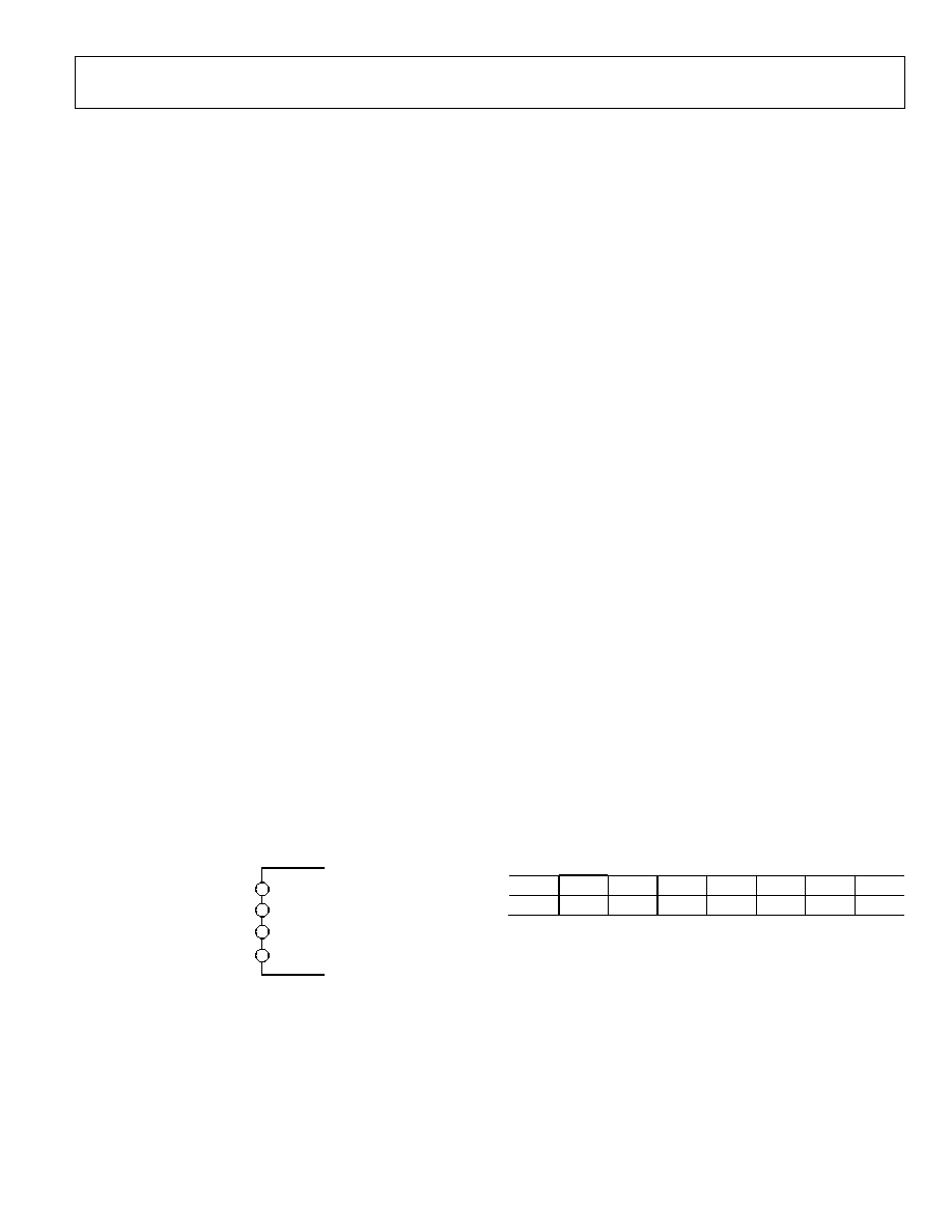
05361-017
Figure 17. AD9779 Third Order IMD vs. f
OUT
, 1× Interpolation
100
50
0
20
40
60
80
100 120 140 160 180 200 220
f
OUT
(MHz)
IMD (dBc
)
90
80
70
60
f
DATA
= 160MSPS
f
DATA
= 250MSPS
f
DATA
= 200MSPS
05361-018
Figure 18. AD9779 Third Order IMD vs. f
OUT
, 2× Interpolation
100
50
0
400
f
OUT
(MHz)
IMD (dBc
)
90
80
70
60
40
80
120
160
200
240
280
320
360
f
DATA
= 150MSPS
f
DATA
= 200MSPS
f
DATA
= 100MSPS
05361-019
Figure 19. AD9779 Third Order IMD vs. f
OUT
, 4× Interpolation
f
OUT
(MHz)
IMD (dBc
)
f
DATA
= 75MSPS
f
DATA
= 125MSPS
f
DATA
= 100MSPS
90
100
80
70
60
50
450
425
400
375
350
325
300
275
250
225
200
175
150
125
100
75
50
25
0
f
DATA
= 50MSPS
05361-020
Figure 20. AD9779 Third Order IMD vs. f
OUT
, 8× Interpolation
100
50
0
200
f
OUT
(MHz)
IMD (dBc
)
90
80
70
60
100
20
40
60
80
120
140
160
180
PLL OFF
PLL ON
05361-021
Figure 21. AD9779 Third Order IMD vs. f
OUT
, 4× Interpolation,
f
DATA
= 100 MSPS, PLL On vs. PLL Off
100
95
50
55
0
400
360
f
OUT
(MHz)
IMD (dBc
)
90
80
85
70
75
60
65
40
80
120
160
200
240
280
320
05361-022
Figure 22. AD9779 Third Order IMD vs. f
OUT
, over 50 Parts,4× Interpolation,
f
DATA
= 200 MSPS

AD9776/AD9778/AD9779
Rev. 0 | Page 17 of 56
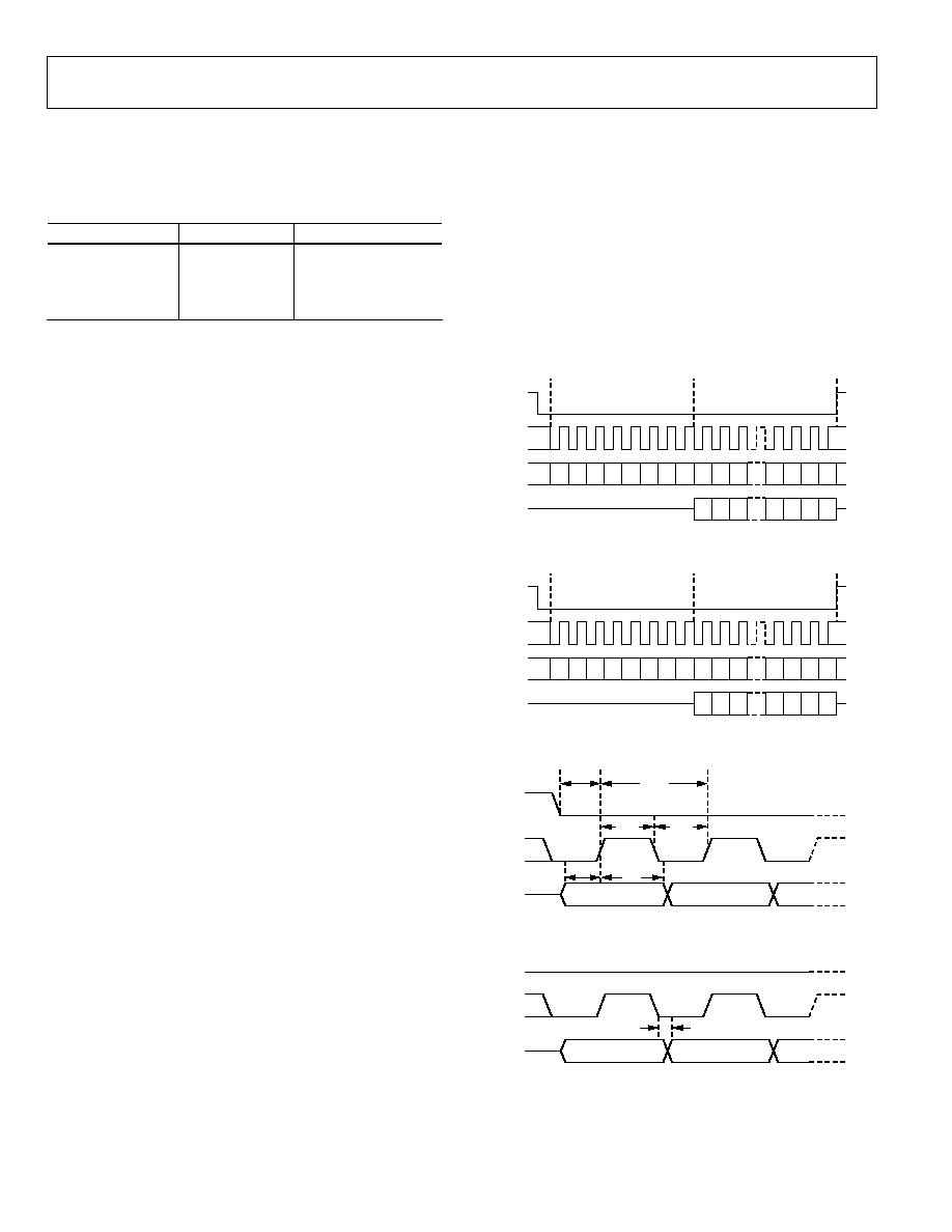
STOP 400.0MHz
SWEEP 1.203s (601 pts)
VBW 20kHz
START 1.0MHz
*RES BW 20kHz
REF 0dBm
*PEAK
Log
10dB/
LGAV
51
W1
S3
Ł(f):
FTUN
SWP
S2
FC
AA
*ATTEN 20dB
EXT REF
DC COUPLED
05361-023
Figure 23. AD9779 Single Tone, 4× Interpolation, f
DATA
= 100 MSPS,
f
OUT
= 30 MHz
STOP 400.0MHz
SWEEP 1.203s (601 pts)
VBW 20kHz
START 1.0MHz
*RES BW 20kHz
REF 0dBm
*PEAK
Log
10dB/
LGAV
51
W1
S3
Ł(f):
FTUN
SWP
S2
FC
AA
*ATTEN 20dB
EXT REF
DC COUPLED
05361-024
Figure 24. AD9779 Two-Tone Spectrum, 4× Interpolation, f
DATA
= 100 MSPS,
f
OUT
= 30,35 MHz
142
146
150
154
158
162
166
170
0
f
OUT
(MHz)
NS
D (dBm/Hz)
20
40
60
80
0dBFS
3dBFS
6dBFS
05361-025
Figure 25. AD9779 Noise Spectral Density vs. Digital Full-Scale of Single-Tone
Input, f
DATA
= 200 MSPS, 2× Interpolation
150
170
0
100
f
OUT
(MHz)
NS
D (dBm/Hz)
154
158
162
166
20
40
60
80
f
DAC
= 800MSPS
f
DAC
= 400MSPS
f
DAC
= 200MSPS
05361-026
Figure 26. AD9779 Noise Spectral Density vs. f
DAC
, Eight-Tone Input
with 500 kHz Spacing, f
DATA
= 200 MSPS
150
170
0
100
f
OUT
(MHz)
NS
D (dBm/Hz)
154
158
162
166
20
40
60
80
f
DAC
= 800MSPS
f
DAC
= 400MSPS
f
DAC
= 200MSPS
05361-027
Figure 27. AD9779 Noise Spectral Density vs. f
DAC
,
Single-Tone Input at 6 dBFS
55
90
0
260
f
OUT
(MHz)
ACLR (dBc
)
60
65
70
75
80
85
20
40
60
80 100 120 140 160 180 200 220 240
6dBFS
3dBFS
0dBFS PLL ON
0dBFS
05361-028
Figure 28. AD9779 ACLR for First Adjacent Band WCDMA, 4× Interpolation,
f
DATA
= 122.88 MSPS, On-Chip Modulation Translates Baseband Signal to IF

AD9776/AD9778/AD9779
Rev. 0 | Page 18 of 56
SPAN 50MHz
SWEEP 162.2ms (601 pts)
VBW 300kHz
CENTER 143.88MHz
*RES BW 30kHz
RMS RESULTS
CARRIER POWER
12.49dBm/
3.84000MHz
FREQ OFFSET
5.000MHz
10.00MHz
15.00MHz
REF BW
3.840MHz
3.840MHz
3.840MHz
dBc
76.75
80.94
79.95
dBm
89.23
93.43
92.44
LOWER
dBc
77.42
80.47
78.96
dBm
89.91
92.96
91.45
UPPER
REF 25.28dBm
*AVG
Log
10dB/
PAVG
10
W1 S2
*ATTEN 4dB
EXT REF
05361-031
Figure 29. AD9779 WCDMA Signal, 4× Interpolation,
f
DATA
=122.88 MSPS, f
DAC
/4 Modulation
55
90
0
260
f
OUT
(MHz)
ACLR (dBc
)
60
65
70
75
80
85
20
40
60
80 100 120 140 160 180 200 220 240
6dBFS
3dBFS
0dBFS PLL ON
0dBFS
05361-030
Figure 30. AD9779 ACLR for Third Adjacent Band WCDMA, 4× Interpolation,
f
DATA
= 122.88 MSPS, On-Chip Modulation Translates Baseband Signal to IF
55
90
0
260
f
OUT
(MHz)
ACLR (dBc
)
60
65
70
75
80
85
20
40
60
80 100 120 140 160 180 200 220 240
6dBFS
3dBFS
0dBFS PLL ON
0dBFS
05361-029
Figure 31. AD9779 ACLR for Second Adjacent Band WCDMA, 4×
Interpolation, f
DATA
= 122.88 MSPS. On-Chip Modulation Translates
Baseband Signal to IF
SPAN 50MHz
SWEEP 162.2ms (601 pts)
VBW 300kHz
CENTER 151.38MHz
*RES BW 30kHz
1 17.87dBm
2 20.65dBm
3 18.26dBm
4 18.23dBm
TOTAL CARRIER POWER 12.61dBm/15.3600MHz
REF CARRIER POWER 17.87dBm/3.84000MHz
FREQ OFFSET
5.000MHz
10.00MHz
15.00MHz
INTEG BW
3.840MHz
3.840MHz
3.840MHz
dBc
67.70
70.00
71.65
dBm
85.57
97.87
99.52
LOWER
dBc
67.70
69.32
71.00
dBm
85.57
87.19
88.88
UPPER
REF 30.28dBm
*AVG
Log
10dB/
PAVG
10
W1 S2
*ATTEN 4dB
EXT REF
05361-032
Figure 32. AD9779 Multicarrier WCDMA Signal, 4× Interpolation,
f
DAC
=122.88 MSPS, f
DAC
/4 Modulation
1.5
0
20k
CODE
INL (14-BIT LSB)
10k
1.0
0.5
0
0.5
1.0
1.5
2k
4k
6k
8k
12k
14k
16k
18k
05361-033
Figure 33. AD778 Typical INL
0.6
0
18k
CODE
DNL (1
4
-
BI
T LS
B)
0.2
1.0
2k
4k
6k
8k
10k
12k
14k
16k
0.4
0.2
0
0.4
0.6
0.8
05361-034
Figure 34. AD9778 Typical DNL
AD9776/AD9778/AD9779
Rev. 0 | Page 19 of 56
100
50
0
400
f
OUT
(MHz)
IMD (dBc
)
90
80
70
60
40
80
120
160
200
240
280
320
360
4
×
200MSPS
4
×
150MSPS
4
×
100MSPS
05361-035
Figure 35. AD9778 IMD, 4× Interpolation
100
50
0
100
f
OUT
(MHz)
S
F
DR (dBc
)
90
80
70
60
20
40
60
80
f
DATA
= 250MSPS
f
DATA
= 200MSPS
f
DATA
= 160MSPS
05361-036
Figure 36. AD9778 In-Band SFDR, 2× Interpolation
90
0
250
f
OUT
(MHz)
ACLR (dBc
)
70
80
60
25
50
75
100
125
150
175
200
225
1ST ADJ CHAN
2ND ADJ CHAN
3RD ADJ CHAN
05361-037
Figure 37. AD9778 ACLR, Single-Carrier WCDMA, 4× Interpolation,
f
DATA
= 122.88 MSPS, Amplitude = 3 dBFS
SPAN 50MHz
SWEEP 162.2ms (601 pts)
VBW 300kHz
CENTER 143.88MHz
*RES BW 30kHz
RMS RESULTS
CARRIER POWER
12.74dBm/
3.84000MHz
FREQ OFFSET
5.000MHz
10.00MHz
15.00MHz
REF BW
3.884MHz
3.840MHz
3.840MHz
dBc
76.49
80.13
80.90
dBm
89.23
92.87
93.64
LOWER
dBc
76.89
80.02
79.53
dBm
89.63
92.76
92.27
UPPER
REF 25.39dBm
*AVG
Log
10dB/
PAVG
10
W1 S2
*ATTEN 4dB
05361-038
Figure 38. AD9778 ACLR, f
DATA
= 122.88 MSPS, 4× Interpolation,
f
DAC
/4 Modulation
150
170
0
100
f
OUT
(MHz)
NS
D (dBm/Hz)
154
158
162
166
20
40
60
80
f
DAC
= 800MSPS
f
DAC
= 400MSPS
f
DAC
= 200MSPS
05361-039
Figure 39. AD9778 Noise Spectral Density vs. f
DAC
Eight-Tone Input
with 500 kHz Spacing, f
DATA
= 200 MSPS
150
170
0
100
f
OUT
(MHz)
NS
D (dBm/Hz)
154
158
162
166
20
40
60
80
f
DAC
= 800MSPS
f
DAC
= 400MSPS
f
DAC
= 200MSPS
05361-040
Figure 40. AD9778 Noise Spectral Density vs. f
DAC
Single-Tone Input
at 6 dBFS, f
DATA
= 200 MSPS
AD9776/AD9778/AD9779
Rev. 0 | Page 20 of 56
0.4
0
4096
CODE
INL (12-BIT LSB)
0.4
512
1024
2560
2048
1536
3072
3584
0.3
0.2
0.1
0
0.1
0.2
0.3
05361-041
Figure 41. AD9776 Typical INL
0.20
0
4096
CODE
DNL (1
2
-
BI
T LS
B)
2048
0.20
512
1024
1536
2560
3072
3584
0.15
0.10
0.05
0
0.05
0.10
0.15
05361-042
Figure 42. AD9776 Typical DNL
100
50
0
400
f
OUT
(MHz)
I
M
D (dBc
)
40
80
120
160
200
240
280
320
360
4
×
200MSPS
4
×
100MSPS
4
×
150MSPS
95
90
85
80
75
70
65
60
55
05361-043
Figure 43. AD9776 IMD, 4× Interpolation
100
50
0
100
f
OUT
(MHz)
S
F
DR (dBc
)
90
80
70
60
20
40
60
80
f
DATA
= 250MSPS
f
DATA
= 200MSPS
f
DATA
= 160MSPS
05361-044
Figure 44. AD9776 In-Band SFDR, 2× Interpolation
90
0
250
f
OUT
(MHz)
ACLR (dBc
)
55
25
50
75
100
125
150
175
200
225
1ST ADJ CHAN
2ND ADJ CHAN
3RD ADJ CHAN
60
65
70
75
80
85
05361-045
Figure 45. AD9776, Single Carrier WCDMA, 4× Interpolation,
f
DATA
= 122.88 MSPS, Amplitude = 3 dBFS
SPAN 50MHz
SWEEP 162.2ms (601 pts)
VBW 300kHz
CENTER 143.88MHz
*RES BW 30kHz
RMS RESULTS
CARRIER POWER
12.67dBm/
3.84000MHz
FREQ OFFSET
5.000MHz
10.00MHz
15.00MHz
REF BW
3.884MHz
3.840MHz
3.840MHz
dBc
75.00
78.05
77.73
dBm
87.67
90.73
90.41
LOWER
dBc
75.30
77.99
77.50
dBm
87.97
90.66
90.17
UPPER
REF 25.29dBm
*AVG
Log
10dB/
PAVG
10
W1 S2
*ATTEN 4dB
05361-046
Figure 46. AD9776 ACLR, f
DATA
= 122.88 MSPS, 4× Interpolation,
f
DAC
/4 Modulation

AD9776/AD9778/AD9779
Rev. 0 | Page 21 of 56
150
170
0
100
f
OUT
(MHz)
NS
D (dBm/Hz)
154
158
162
166
20
40
60
80
f
DAC
= 800MSPS
f
DAC
= 400MSPS
f
DAC
= 200MSPS
10
30
50
70
90
05361-047
Figure 47. AD9776 Noise Spectral Density vs. f
DAC
, Eight-Tone Input
with 500 kHz Spacing, f
DATA
= 200 MSPS
150
170
0
100
f
OUT
(MHz)
NS
D (dBm/Hz)
154
158
162
166
20
40
60
80
f
DAC
= 800MSPS
f
DAC
= 400MSPS
f
DAC
= 200MSPS
10
30
50
70
90
05361-048
Figure 48. AD9776 Noise Spectral Density vs. f
DAC
,
Single-Tone Input at 6 dBFS, f
DATA
= 200 MSPS

AD9776/AD9778/AD9779
Rev. 0 | Page 22 of 56
TERMINOLOGY
Linearity Error (Integral Nonlinearity or INL)
Linearity error is defined as the maximum deviation of the
actual analog output from the ideal output, determined by a
straight line drawn from zero scale to full scale.
Differential Nonlinearity (DNL)
DNL is the measure of the variation in analog value, normalized
to full scale, associated with a 1 LSB change in digital input
code.
Monotonicity
A DAC is monotonic if the output either increases or remains
constant as the digital input increases.
Offset Error
The deviation of the output current from the ideal of zero is
called offset error. For I
OUTA
, 0 mA output is expected when the
inputs are all 0s. For I
OUTB
, 0 mA output is expected when all
inputs are set to 1.
B
Gain Error
The difference between the actual and ideal output span. The
actual span is determined by the difference between the output
when all inputs are set to 1 and the output when all inputs are
set to 0.
Output Compliance Range
The range of allowable voltage at the output of a current-output
DAC. Operation beyond the maximum compliance limits can
cause either output stage saturation or breakdown, resulting in
nonlinear performance.
Temperature Drift
Temperature drift is specified as the maximum change from the
ambient (25°C) value to the value at either T
MIN
or T
MAX
. For
offset and gain drift, the drift is reported in ppm of full-scale
range (FSR) per degree Celsius. For reference drift, the drift is
reported in ppm per degree Celsius.
Power Supply Rejection
The maximum change in the full-scale output as the supplies
are varied from minimum to maximum specified voltages.
Settling Time
The time required for the output to reach and remain within a
specified error band around its final value, measured from the
start of the output transition.
In-Band Spurious Free Dynamic Range (SFDR)
The difference, in decibels, between the peak amplitude of the
output signal and the peak spurious signal between dc and the
frequency equal to half the input data rate.
Out-of-Band Spurious Free Dynamic Range (SFDR)
The difference, in decibels, between the peak amplitude of the
output signal and the peak spurious signal within the band that
starts at the frequency of the input data rate and ends at the
Nyquist frequency of the DAC output sample rate. Normally,
energy in this band is rejected by the interpolation filters. This
specification therefore defines how well the interpolation filters
work and the effect of other parasitic coupling paths to the DAC
output.
Total Harmonic Distortion (THD)
THD is the ratio of the rms sum of the first six harmonic com-
ponents to the rms value of the measured fundamental. It is
expressed as a percentage or in decibels.
Signal-to-Noise Ratio (SNR)
SNR is the ratio of the rms value of the measured output signal
to the rms sum of all other spectral components below the
Nyquist frequency, excluding the first six harmonics and dc.
The value for SNR is expressed in decibels.
Interpolation Filter
If the digital inputs to the DAC are sampled at a multiple rate of
f
DATA
(interpolation rate), a digital filter can be constructed that
has a sharp transition band near f
DATA
/2. Images that typically
appear around f
DAC
(output data rate) can be greatly suppressed.
Adjacent Channel Leakage Ratio (ACLR)
The ratio in dBc between the measured power within a channel
relative to its adjacent channel.
Complex Image Rejection
In a traditional two-part upconversion, two images are created
around the second IF frequency. These images have the effect of
wasting transmitter power and system bandwidth. By placing
the real part of a second complex modulator in series with the
first complex modulator, either the upper or lower frequency
image near the second IF can be rejected.
AD9776/AD9778/AD9779
Rev. 0 | Page 23 of 56
THEORY OF OPERATION
The AD9776/AD9778/AD9779 combine many features that
make them very attractive DACs for wired and wireless
communications systems. The dual digital signal path and dual
DAC structure allow an easy interface with common quadra-
ture modulators when designing single sideband transmitters.
The speed and performance of the parts allow wider band-
widths and more carriers to be synthesized than in previously
available DACs. The digital engine uses a breakthrough filter
architecture that combines the interpolation with a digital
quadrature modulator. This allows the parts to do digital
quadrature frequency upconversion. They also have features
that allow simplified synchronization with incoming data and
between multiple parts.
The serial port configuration is controlled by Reg. 0x00,
Bits <6: 7>. It is important to note that the configuration
changes immediately upon writing to the last bit of the byte.
For multibyte transfers, writing to this register might occur
during the middle of a communication cycle. Care must be
taken to compensate for this new configuration for the
remaining bytes of the current communication cycle.
The same considerations apply to setting the software reset,
RESET (Reg. 0x00, Bit 5) or pulling the RESET pin (Pin 70)
high. All registers are set to their default values, except
Reg. 0x00 and Reg. 0x04, which remain unchanged.
Use of only single-byte transfers when changing serial port
configurations or initiating a software reset is recommended to
prevent unexpected device behavior.
As described in this section, all serial port data is transferred
to/from the device in synchronization to the SCLK pin. If
synchronization is lost, the device has the ability to asynchro-
nously terminate an I/O operation, putting the serial port
controller into a known state and thereby regaining synchro-
nization.
SERIAL PERIPHERAL INTERFACE
SPI_SDO
SPI
PORT
66
SPI_SDI
67
SPI_SCLK
68
SPI_CSB
69
05361-049
Figure 49. SPI Port
The serial port is a flexible, synchronous serial communications
port allowing easy interface to many industry-standard micro-
controllers and microprocessors. The serial I/O is compatible
with most synchronous transfer formats, including both the
Motorola SPI
®
and Intel
®
SSR protocols. The interface allows
read/write access to all registers that configure the AD9776/
AD9778/AD9779. Single or multiple byte transfers are sup-
ported, as well as MSB-first or LSB-first transfer formats. The
serial interface ports can be configured as a single pin I/O (SDIO)
or two unidirectional pins for input/output (SDIO/SDO).
General Operation of the Serial Interface
There are two phases to a communication cycle with the
AD977x. Phase 1 is the instruction cycle, which is the writing of
an instruction byte into the device, coincident with the first
eight SCLK rising edges. The instruction byte provides the
serial port controller with information regarding the data
transfer cycle, which is Phase 2 of the communication cycle.
The Phase 1 instruction byte defines whether the upcoming
data transfer is a read or write, the number of bytes in the data
transfer, and the starting register address for the first byte of the
data transfer. The first eight SCLK rising edges of each commu-
nication cycle are used to write the instruction byte into the
device.
A logic high on the CSB pin followed by a logic low resets the
SPI port timing to the initial state of the instruction cycle.
From this state, the next eight rising SCLK edges represent the
instruction bits of the current I/O operation, regardless of the
state of the internal registers or the other signal levels at the
inputs to the SPI port. If the SPI port is in the midst of an
instruction cycle or a data transfer cycle, none of the present
data is written.
The remaining SCLK edges are for Phase 2 of the communi-
cation cycle. Phase 2 is the actual data transfer between the
device and the system controller. Phase 2 of the communication
cycle is a transfer of 1, 2, 3, or 4 data bytes as determined by the
instruction byte. Using one multibyte transfer is preferred.
Single-byte data transfers are useful to reduce CPU overhead
when register access requires only one byte. Registers change
immediately upon writing to the last bit of each transfer byte.
Instruction Byte
The instruction byte contains the information shown in
Table 8.
Table 8. SPI Instruction Byte
MSB
LSB
I7 I6 I5 I4 I3 I2 I1 I0
R/W
N1 N0 A4 A3 A2 A1 A0
R/W, Bit 7 of the instruction byte, determines whether a read or
a write data transfer occurs after the instruction byte write.
Logic high indicates a read operation. Logic 0 indicates a write
operation.
N1 and N0, Bits 6 and 5 of the instruction byte, determine the
number of bytes to be transferred during the data transfer cycle.
The bit decodes are shown in Table 9.
A4, A3, A2, A1, and A0--Bits 4, 3, 2, 1, and 0, respectively, of
the instruction byte--determine which register is accessed
AD9776/AD9778/AD9779
Rev. 0 | Page 24 of 56
during the data transfer portion of the communications cycle.
For multibyte transfers, this address is the starting byte address.
The remaining register addresses are generated by the device
based on the LSB-first bit (Reg. 0x00, Bit 6).
Table 9. Byte Transfer Count
N0 N1
Description
0
0
Transfer one byte
0
1
Transfer two bytes
1
0
Transfer three bytes
1
1
Transfer four bytes
Serial Interface Port Pin Descriptions
Serial Clock (SCLK)
The serial clock pin is used to synchronize data to and from the
device and to run the internal state machines. SCLK's maxi-
mum frequency is 40 MHz. All data input is registered on the
rising edge of SCLK. All data is driven out on the falling edge of
SCLK.
Chip Select (CSB)
Active low input starts and gates a communication cycle. It
allows more than one device to be used on the same serial
communications lines. The SDO and SDIO pins go to a high
impedance state when this input is high. Chip select should stay
low during the entire communication cycle.
Serial Data I/O (SDIO)
Data is always written into the device on this pin. However, this
pin can be used as a bidirectional data line. The configuration
of this pin is controlled by Register 0x00, Bit 7. The default is
Logic 0, which configures the SDIO pin as unidirectional.
Serial Data Out (SDO)
Data is read from this pin for protocols that use separate lines
for transmitting and receiving data. In the case where the device
operates in a single bidirectional I/O mode, this pin does not
output data and is set to a high impedance state.
MSB/LSB TRANSFERS
The serial port can support both MSB-first and LSB-first data
formats. This functionality is controlled by Register Bit LSB first
(Reg. 0x00, Bit 6). The default is MSB first (LSB first = 0).
When LSB first = 0 (MSB first) the instruction and data bit
must be written from MSB to LSB. Multibyte data transfers in
MSB-first format start with an instruction byte that includes the
register address of the most significant data byte. Subsequent
data bytes should follow from high address to low address. In
MSB-first mode, the serial port internal byte address generator
decrements for each data byte of the multibyte communication
cycle.
When LSB first = 1 (LSB first) the instruction and data bit must
be written from LSB to MSB. Multibyte data transfers in LSB-
first format start with an instruction byte that includes the
register address of the least significant data byte followed by
multiple data bytes. The serial port internal byte address gener-
ator increments for each byte of the multibyte communication
cycle.
The serial port controller data address decrements from the
data address written toward 0x00 for multibyte I/O operations if
the MSB-first mode is active. The serial port controller address
increments from the data address written toward 0x1F for
multibyte I/O operations if the LSB-first mode is active.
R/W N1 N0 A4 A3
A2 A1 A0 D7 D6
N
D5
N
D0
0
D1
0
D2
0
D3
0
D7 D6
N
D5
N
D0
0
D1
0
D2
0
D3
0
INSTRUCTION CYCLE
DATA TRANSFER CYCLE
CSB
SCLK
SDIO
SDO
05361-050
Figure 50. Serial Register Interface Timing MSB First
A0 A1 A2 A3 A4
N0 N1 R/W D0
0
D1
0
D2
0
D7
N
D6
N
D5
N
D4
N
D0
0
D1
0
D2
0
D7
N
D6
N
D5
N
D4
N
INSTRUCTION CYCLE
DATA TRANSFER CYCLE
CSB
SCLK
SDIO
SDO
05361-051
Figure 51. Serial Register Interface Timing LSB First
INSTRUCTION BIT 6
INSTRUCTION BIT 7
CSB
SCLK
SDIO
t
DS
t
DS
t
DH
t
PWH
t
PWL
t
SCLK
05361-052
Figure 52. Timing Diagram for SPI Register Write
DATA BIT n1
DATA BIT n
CSB
SCLK
SDIO
SDO
t
DV
05361-053
Figure 53. Timing Diagram for SPI Register Read

AD9776/AD9778/AD9779
Rev. 0 | Page 25 of 56
SPI REGISTER MAP
Table 10.
Register
Name
Address
Bit 7
Bit 6
Bit 5
Bit 4
Bit 3
Bit 2
Bit 1
Bit 0
Def.
Comm 0x00
00 SDIO
Bidirectional
LSB/MSB First
Software
Reset
Power-Down
Mode
Auto Power-
Down Enable
PLL
Lock
Indicator
(Read Only)
0x00
Digital
Control
0x01 01
Filter Interpolation Factor <1:0>
Filter Modulation Mode <3:0>
Zero
Stuffing
Enable
0x00
0x02
02
Data
Format
Dual/Interleaved
Data Bus Mode
Real Mode
Data Clock
Delay Enable
Inverse Sinc
Enable
DATACLK
Invert
TxEnable
Invert
Q First
0x00
Sync
Control
0x03 03
Data Clock Delay Mode <1:0>
Data Clock Divide Ratio <1:0>
Reserved
0x00
0x04 04
Data Clock Delay <3:0>
Output Sync Pulse Divide <2:0>
Sync Out
Delay <4>
0x00
0x05 05
Sync Out Delay <3:0>
Input Sync Pulse Frequency Ratio <2:0> Sync Input
Delay <4>
0x00
0x06 06
Sync Input Delay <3:0>
Input Sync Pulse Timing Error Tolerance <3:0>
0x00
0x07
07
Sync
Receiver
Enable
Sync Driver
Enable
Sync
Triggering
Edge
DAC Clock Offset <4:0>
0x00
PLL Control 0x08 08
PLL Band Select <5:0>
PLL VCO AGC Gain
<1:0>
0xCF
0x09 09
PLL Enable
PLL VCO Divider Ratio <1:0>
PLL Loop Divide Ratio <1:0> PLL Bias Setting <2:0>
0x37
Misc
Control
0x0A 10
PLL Control Voltage Range <2:0> (Read Only)
PLL Loop Bandwidth Adjustment <4:0>
0x38
0x0B 11
I DAC Gain Adjustment<7:0>
0xF9
I DAC
Control
Register
0x0C 12
I DAC Sleep
I DAC Power
Down
I DAC Gain Adjustment
<9:8>
0x01
Aux DAC1
Control
Register
0x0D 13
Auxiliary DAC1 Data <7:0>
0x00
0x0E
14
Auxiliary
DAC1
Sign
Auxiliary DAC1
Current
Direction
Auxiliary DAC1
Power-Down
Auxiliary DAC1 Data
<9:8>
0x00
Q DAC
Control
Register
0x0F 15
Q DAC Gain Adjustment <7;0>
0xF9
0x10 16
Q DAC Sleep
Q DAC Power-
Down
Q DAC Gain Adjustment
<9:8>
0x01
Aux DAC2
Control
Register
0x11 17
Auxiliary DAC2 Data <7:0>
0x00
0x12
18
Auxiliary
DAC2
Sign
Auxiliary DAC2
Current
Direction
Auxiliary DAC2
Power-Down
Auxiliary DAC2 Data
<9:8>
0x00
0x13
to
0x18
19 to
24
Reserved
Interrupt
Register
0x19 25
Sync Delay IRQ
Sync Delay
IRQ Enable
Internal
Sync
Loopback
0x00
0x1A
to
0x1F
26 to
31
Reserved

AD9776/AD9778/AD9779
Rev. 0 | Page 26 of 56
Table 11. SPI Register Description
Address
Register Name
Hex
Decimal
Name
Function
Default
Comm Register
00
7
SDIO Bidirectional
0: Use SDIO pin as input data only
1: Use SDIO as both input and output data
0
00
6
LSB/MSB
First
0: First bit of serial data is MSB of data byte
1: First bit of serial data is LSB of data byte
0
00
5
Software
Reset
Bit must be written with a 1, then 0 to soft reset
SPI register map
0
00
4
Power-Down
Mode
0: All circuitry is active
1: Disable all digital and analog circuitry, only SPI
port is active
00
3
Auto Power-Down Enable
Controls auto power-down mode, see Power-
Down and Sleep Modes section
0
00
1
PLL Lock (Read Only)
0: PLL is not locked
1: PLL is locked
0
Digital Control
Register
01
7:6
Filter Interpolation Factor
00:1× interpolation
01:2× interpolation
10:4× interpolation
11:8× interpolation
00
01
5:2
Filter Modulation Mode
See Table 19 for filter modes
0000
01
0
Zero
Stuffing
0: Zero stuffing off
1: Zero stuffing on
0
02
7
Data
Format
0: Signed binary
1: Unsigned binary
0
02
6
Dual/Interleaved Data Bus
Mode
0: Both input data ports receive data
1: Data port 1 only receives data
0
02
5
Real
Mode
0: Enable Q path for signal processing
1: Disable Q path data (internal Q channel clocks
disabled, I and Q modulators disabled)
0
02
3
Inverse Sinc Enable
0: Inverse sinc filter disabled
1: Inverse sinc filter enabled
0
02
2
DATACLK
Invert
0: Output DATACLK same phase as internal
capture clock
1: Output DATACLK opposite phase as internal
capture clock
0
02
1
TxEnable
Invert
Inverts the function of TxEnable Pin 39, see
Interleaved Data Mode section
0
02
0
Q
First 0: First byte of data is always I data at beginning
of transmit
1: First byte of data is always Q data at beginning
of transmit
Sync Control Register
03
7:6
Data Clock Delay Mode
00: Manual, no error correction
00
03
5:4
Extra Data Clock Divide Ratio
Data Clock Output Divider (see Table 22 for
Divider Ratio)
00
03
3:0
Reserved
000
04
7:4
Data Clock Delay
Sets delay of DACCLK in to DATACLK out
0000
04
3:1
Output Sync Pulse Divide
Sets frequency of Sync_O pulses
000
04
0
Sync Out Delay
Sync Output Delay, Bit 4
05
7:4
Sync Out Delay
Sync Output Delay, Bit <3:0>
0
05
3:1
Input Sync Pulse Frequency
Input Sync Pulse Frequency Divider, see the
Sync Pulse Receiver (Slave Devices) section
000
05
0
Sync Input Delay
Sync Input Delay, Bit 4
0
AD9776/AD9778/AD9779
Rev. 0 | Page 27 of 56
Address
Register Name
Hex
Decimal
Name
Function
Default
Sync Control Register
06
7:4
Sync Input Delay
See Multi-DAC Synchronization section for
details on using these registers to synchronize
multiple DACs.
0
06
3:0
Input Sync Pulse Timing Error
Tolerance
0
07
7
Sync Receiver Enable
0
07
6
Sync Driver Enable
0
07
5
Sync
Triggering
Edge
0
07
4:0
Sync_I to Input Data
Sampling Clock Offset
0
PLL Control
08
7:2
PLL Band Select
VCO frequency range vs. PLL band select value
(see Table 17)
110011
08
1:0
VCO AGC Gain Control
Lower number (low gain) is generally better for
performance.
11
09
7
PLL
Enable
0: PLL off, DAC rate clock supplied by outside
source
1: PLL on, DAC rate clock synthesized internally
from external reference clock via PLL clock
multiplier
0
09
6:5
PLL VCO Divide Ratio
FVCO/f
DAC
00 × 1
01 × 2
10 × 4
11 × 8
09
4:3
PLL Loop Divide Ratio
f
DAC
/f
REF
00 × 2
01 × 4
10 × 8
11 × 16
09
2:0
PLL Bias Setting
Always set to 111
111
Misc Control
0A
7:5
PLL Control Voltage Range
000 to 111, proportional to voltage at PLL loop
filter output, readback only
0A
4:0
PLL Loop Bandwidth
Adjustment
See PLL Loop Filter Bandwidth section for details
I DAC Control Register
0B
7:0
I DAC Gain Adjustment
(7:0) LSB slice of 10-bit gain setting word
for I DAC
11111001
0C
7
I DAC Sleep
0: I DAC on
1: I DAC off
0
0C
6
I DAC Power-Down
0: I DAC on
1: I DAC off
0
0C
1:0
I DAC Gain Adjustment
(9:8) MSB slice of 10-bit gain setting word
for I DAC
01
Aux DAC1 Control
Register
0D
7:0
Aux DAC1 Gain Adjustment
(7:0) LSB slice of 10-bit gain setting word for Aux
DAC1
00000000
0E
7
Aux DAC1 Sign
0: Positive
1: Negative
0E
6
Aux DAC1 Current Direction
0: Source
1: Sink
0
0E
5
Aux DAC1 Power-Down
0: Aux DAC1 on
1: Aux DAC1 off
0
0E
1:0
Aux DAC1 Gain Adjustment
(9:8) MSB slice of 10 bit gain setting word for Aux
DAC1
00
AD9776/AD9778/AD9779
Rev. 0 | Page 28 of 56
Address
Register Name
Hex
Decimal
Name
Function
Default
Q DAC Control
Register
0F
7:0
Q DAC Gain Adjustment
(7:0) LSB slice of 10-bit gain setting word for Q
DAC
11111001
10
7
Q DAC Sleep
0: Q DAC on
1: Q DAC off
0
10
6
Q DAC Power-Down
0: Q DAC on
1: Q DAC off
0
10
1:0
Q DAC Gain Adjustment
(9:8) MSB slice of 10-bit gain setting word for Q
DAC
Aux DAC2 Control
Register
11
7:0
Aux DAC2 Gain Adjustment
(7:0) LSB slice of 10-bit gain setting word for Aux
DAC2
00000000
12
7
Aux DAC2 Sign
0: Positive
1: Negative
12
6
Aux DAC2 Current Direction
0: Source
1: Sink
0
12
5
Aux DAC2 Power-Down
0: Aux DAC 2 on
1: Aux DAC 2 off
0
12
1:0
Aux DAC2 Gain Adjustment
(9:8) MSB slice of 10-bit gain setting word for
Aux DAC2
00
Interrupt Register
19
7
0
19
6
Sync Delay IRQ
Readback , must write 0 to clear
0
19
5
0
19
3
0
19
2
Sync Delay IRQ Enable
0
19
1
0
19
0
Internal Sync Loopback
0
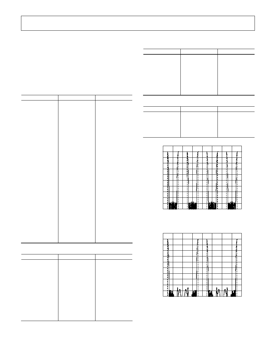
AD9776/AD9778/AD9779
Rev. 0 | Page 29 of 56
INTERPOLATION FILTER ARCHITECTURE
The AD9776/AD9778/AD9779 can provide up to 8× interpola-
tion or disable the interpolation filters entirely. It is important
to note that the input signal should be backed off by approxima-
tely 0.01 dB from full scale to avoid overflowing the interpola-
tion filters. The coefficients of the low-pass filters and the
inverse sinc filter are given in Table 12, Table 13, Table 14,and
Table 15. Spectral plots for the filter responses are shown in
Figure 54, Figure 55, and Figure 56.
Table 12. Halfband Filter 1
Lower Coefficient
Upper Coefficient Integer
Value
H(1) H(55)
4
H(2) H(54)
0
H(3) H(53)
13
H(4) H(52)
0
H(5) H(51)
34
H(6) H(50)
0
H(7) H(49)
72
H(8) H(48)
0
H(9) H(47)
138
H(10) H(46) 0
H(11) H(45) 245
H(12) H(44) 0
H(13) H(43) 408
H(14) H(42) 0
H(15) H(41) 650
H(16) H(40) 0
H(17) H(39) 1003
H(18) H(38) 0
H(19) H(37) 1521
H(20) H(36) 0
H(21) H(35) 2315
H(22) H(34) 0
H(23) H(33) 3671
H(24) H(32) 0
H(25) H(31) 6642
H(26) H(30) 0
H(27) H(29) 20755
H(28)
32768
Table 13. Halfband Filter 2
Lower Coefficient
Upper Coefficient Integer
Value
H(1) H(23)
2
H(2) H(22)
0
H(3) H(21)
17
H(4) H(20)
0
H(5) H(19)
75
H(6) H(18)
0
H(7) H(17)
238
H(8) H(16)
0
H(9) H(15)
660
H(10) H(14) 0
H(11) H(13) 2530
H(12)
4096
Table 14. Halfband Filter 3
Lower Coefficient
Upper Coefficient Integer
Value
H(1) H(15)
39
H(2) H(14)
0
H(3) H(13)
273
H(4) H(12)
0
H(5) H(11)
1102
H(6) H(10)
0
H(7) H(9) 4964
H(8)
8192
Table 15. Inverse Sinc Filter
Lower Coefficient
Upper Coefficient Integer
Value
H(1) H(9) 2
H(2) H(8) 4
H(3) H(7) 10
H(4) H(6) 35
H(5)
401
10
100
4
4
f
OUT
(
×
Input Data Rate)
ATTE
NUATION (dB)
3
2
1
0
1
2
3
0
10
20
30
40
50
60
70
80
90
05361-054
Figure 54. 2× Interpolation, Low-Pass Response to ±4× Input Data Rate
(Dotted Lines Indicate 1 dB Roll-Off)
10
100
4
4
f
OUT
(
×
Input Data Rate)
ATTE
NUATION (dB)
3
2
1
0
1
2
3
0
10
20
30
40
50
60
70
80
90
05361-055
Figure 55. 4× Interpolation, Low-Pass Response to ±4× Input Data Rate
(Dotted Lines Indicate 1 dB Roll-Off)
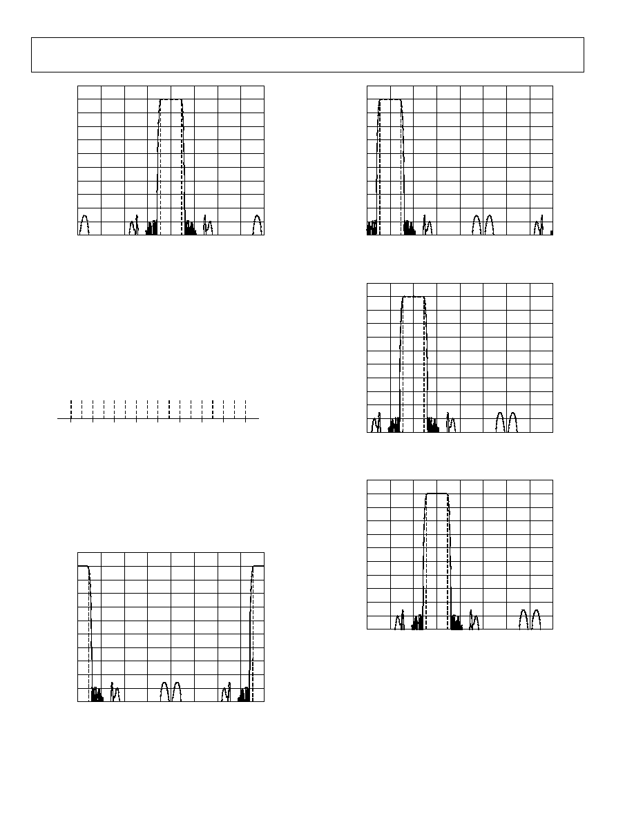
AD9776/AD9778/AD9779
Rev. 0 | Page 30 of 56
10
100
4
4
f
OUT
(
×
Input Data Rate)
ATTE
NUATION (dB)
3
2
1
0
1
2
3
0
10
20
30
40
50
60
70
80
90
05361-056
Figure 56. 8× Interpolation, Low-Pass Response to ±4× Input Data Rate
(Dotted Lines Indicate 1 dB Roll-Off)
With the interpolation filter and modulator combined, the
incoming signal can be placed anywhere within the Nyquist
region of the DAC output sample rate. When the input signal is
complex, this architecture allows modulation of the input signal
to positive or negative Nyquist regions (see Table 16).
The Nyquist regions of up to 4× the input data rate can be seen
in Figure 57.
4
×
8
3
×
6
2
×
4
1
×
2
DC
1
1
×
3
2
×
5
3
×
7
7
5
3
1
2
4
6
8
4
×
05361-057
Figure 57. Nyquist Zones
Figure 54, Figure 55, and Figure 56 show the low-pass response
of the digital filters with no modulation used. By turning on the
modulation feature, the response of the digital filters can be
tuned to anywhere within the DAC bandwidth. As an example,
Figure 58 to Figure 64 show the nonshifted mode filter res-
ponses (refer to Table 16 for shifted/nonshifted mode filter
responses).
10
100
4
4
3
2
1
0
1
2
3
0
10
20
30
40
50
60
70
80
90
f
OUT
(
×
Input Data Rate)
ATTE
NUATION (dB)
05361-058
Figure 58. Interpolation/Modulation Combination of 4f
DAC
/8 Filter
10
100
4
4
3
2
1
0
1
2
3
0
10
20
30
40
50
60
70
80
90
f
OUT
(
×
Input Data Rate)
ATTE
NUATION (dB)
05361-059
Figure 59. Interpolation/Modulation Combination of 3f
DAC
/8 Filter
10
100
4
4
3
2
1
0
1
2
3
0
10
20
30
40
50
60
70
80
90
f
OUT
(
×
Input Data Rate)
ATTE
NUATION (dB)
05361-060
Figure 60. Interpolation/Modulation Combination of 2f
DAC
/8 Filter
10
100
4
4
3
2
1
0
1
2
3
0
10
20
30
40
50
60
70
80
90
f
OUT
(
×
Input Data Rate)
ATTE
NUATION (dB)
05361-061
Figure 61. Interpolation/Modulation Combination of 1f
DAC
/8 Filter
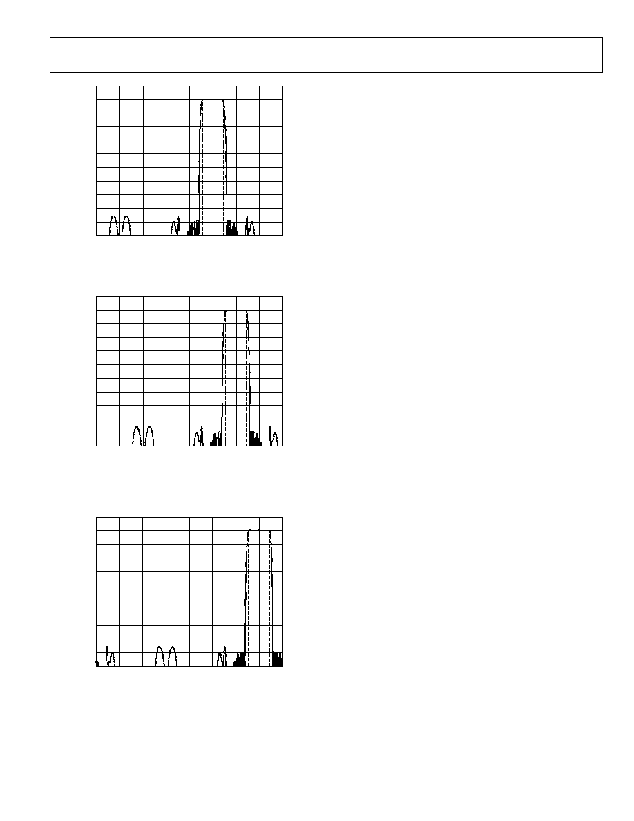
AD9776/AD9778/AD9779
Rev. 0 | Page 31 of 56
10
100
4
4
3
2
1
0
1
2
3
0
10
20
30
40
50
60
70
80
90
f
OUT
(
×
Input Data Rate)
ATTE
NUATION (dB)
05361-062
Figure 62. Interpolation/Modulation Combination of f
DAC
/8 Filter
10
100
4
4
3
2
1
0
1
2
3
0
10
20
30
40
50
60
70
80
90
f
OUT
(
×
Input Data Rate)
f
OUT
(
×
Input Data Rate)
05361-063
Figure 63. Interpolation/Modulation Combination of
2f
DAC
/8 Filter in Odd Mode
10
100
4
4
3
2
1
0
1
2
3
0
10
20
30
40
50
60
70
80
90
f
OUT
(
×
Input Data Rate)
ATTE
NUATION (dB)
05361-064
Figure 64. Interpolation/Modulation Combination of
3f
DAC
/8 Filter in Odd Mode
Shifted mode filter responses allow the pass band to be centered
around ±0.5, ±1.5, ±2.5, and ±3.5 f
DATA
. Switching to the shifted
mode response does not modulate the signal. Instead, the pass
band is simply shifted. For example, picture the response shown
in Figure 64 and assume the signal in-band is a complex signal
over the bandwidth 3.2 f
DATA
to 3.3 f
DATA
. If the even mode filter
response is then selected, the pass band becomes centered at
3.5 f
DATA
. However, the signal remains at the same place in the
spectrum. The shifted mode capability allows the filter pass
band to be placed anywhere in the DAC Nyquist bandwidth.
The AD9776/AD9778/AD9779 are dual DACs with internal
complex modulators built into the interpolating filter response.
In dual channel mode, the devices expect the real and the
imaginary components of a complex signal at Digital Input
Port 1 and Digital Input Port 2 (I and Q respectively). The DAC
outputs then represent the real and imaginary components of
the input signal, modulated by the complex carrier f
DAC
/2,
f
DAC
/4, or f
DAC
/8.
With Reg. 2, Bit 6 set, the device accepts interleaved data on
Port 1 in the I, Q, I, Q ... sequence. Note that in interleaved
mode, the channel data rate at the beginning of the I and the Q
data paths are now half the input data rate because of the inter-
leaving. The maximum input data rate is still subject to the
maximum specification of the device. This limits the synthesis
bandwidth available at the input in interleaved mode.
With Reg. 0x02, Bit 5 (real mode) set, the Q channel and the
internal I and Q digital modulation are turned off. The output
spectrum at the I DAC then represents the signal at Digital
Input Port 1, interpolated by 1×, 2×, 4×, or 8×.
The general recommendation is that if the desired signal is
within ±0.4 × f
DATA
, the odd filter mode should be used. Outside
of this, the even filter mode should be used. In any situation, the
total bandwidth of the signal should be less than 0.8 × f
DATA
.
AD9776/AD9778/AD9779
Rev. 0 | Page 32 of 56
Table 16. Interpolation Filter Modes, (Reg. 0x01, Bits <5:2>)
Interpolation
Factor <7:6>
Filter
Mode
<5:2>
Modulation
Nyquist
Zone
Pass
Band
F_Low
1
Center
1
F_High
1
Comments
8 0x00
DC
1
0.05
0
+0.05
8
0x01 DC
shifted 2
0.0125 0.0625 0.1125
8 0x02
F/8
3
0.075
0.125
0.175
8 0x03
F/8
shifted
4
0.1375
0.1875
0.2375
8 0x04
F/4
5
0.2
0.25
0.3
8 0x05
F/4
shifted
6
0.2625
0.3125
0.3625
8 0x06
3F/8
7
0.325
0.375
0.425
8 0x07
3F/8
shifted
8
0.3875
0.4375
0.4875
8 0x08
F/2
8
0.55
0.5
0.45
8 0x09
F/2
shifted
7
0.4875
0.4375
0.3875
8
0x0A 3F/8
6
0.425 0.375 0.343
8 0x0B
3F/8
shifted
5
0.3625
0.3125
0.2625
8 0x0C
F/4
4
0.3
0.25
0.2
8 0x0D
F/4
shifted
3
0.2375
0.1875
0.1375
8 0x0E
F/8
2
0.175
0.125
0.075
8 0x0F
F/8
shifted
-1
0.1125
0.0625
0.0125
In 8× interpolation; BW (min)
= 0.0375 × f
DAC
BW (max) =
0.1 × f
DAC
4 0x00
DC
1
0.1
0
+0.1
4 0x01
DC
shifted
2
0.025
0.125
0.225
4 0x02
F/4
3
0.15
0.25
0.35
4 0x03
F/4
shifted
4
0.275
0.375
0.475
4 0x04
F/2
4
0.6
0.5
0.4
4 0x05
F/2
shifted
3
0.475
0.375
0.275
4 0x06
F/4
2
0.35
0.25
0.15
4 0x07
F/4
shifted
1
0.225
0.125
0.025
In 4× interpolation; BW (min)
= 0.075 × f
DAC
BW (max) =
0.2 × f
DAC
2 0x00
DC
1
0.2
0
0.2
2 0x01
DC
shifted
2
0.05
0.25
0.45
2 0x02
F/2
2
0.7
0.5
0.3
2 0x03
F/2
shifted
1
0.45
0.25
0.05
In 2× interpolation; BW (min)
= 0.15 × f
DAC
BW (max) =
0.4 × f
DAC
1
Frequency normalized to f
DAC
.
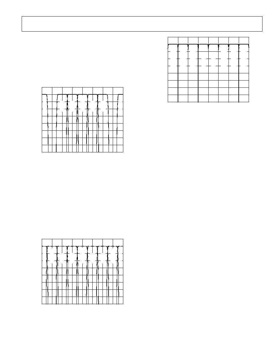
AD9776/AD9778/AD9779
Rev. 0 | Page 33 of 56
INTERPOLATION FILTER MINIMUM AND
MAXIMUM BANDWIDTH SPECIFICATIONS
The AD977x uses a novel interpolation filter architecture that
allows DAC IF frequencies to be generated anywhere in the
spectrum. Figure 65 shows the traditional choice of DAC IF
output bandwidth placement. Note that there are no possible
filter modes in which the carrier can be placed near 0.5 × f
DATA
,
1.5 × f
DATA
, 2.5 × f
DATA
, etc.
10
80
4
4
f
OUT
(
×
Input Data Rate),
ASSUMING 8
×
INTERPOLATION
ATTE
NUATION (dB)
0
10
20
30
40
50
60
70
3
2
1
0
1
2
3
+
f
DAC
/2
+
f
DAC
/4
+
f
DAC
/8
BAS
E
BAND
f
DAC
/8
f
DAC
/4
f
DAC
/2
05361-065
Figure 65. Traditional Bandwidth Options for TxDAC Output IF
The filter architecture not only allows the interpolation filter
pass bands to be centered in the middle of the input Nyquist
zones (as explained in this section), but also allows the
possibility of a 3 × f
DAC
/8 modulation mode. With all of these
filter combinations, a carrier of given bandwidth can be placed
anywhere in the spectrum and fall into a possible pass band of
the interpolation filters. The possible bandwidths accessible
with the filter architecture are shown in Figure 66 and
Figure 67. Note that the shifted and nonshifted filter modes
are all accessible by programming the filter mode for the
particular interpolation rate.
10
80
4
4
f
OUT
(
×
Input Data Rate),
ASSUMING 8
×
INTERPOLATION
ATTE
NUATION (dB)
0
10
20
30
40
50
60
70
3
2
1
0
1
2
3
f
DAC
/2
3
×
f
DAC
/8
f
DAC
/4
f
DAC
/8
BAS
E
BAND
+
f
DAC
/8
+
f
DAC
/4
3
×
f
DAC
/8
+
f
DAC
/2
05361-066
Figure 66. Nonshifted Bandwidths Accessible with the Filter Architecture
10
80
4
4
f
OUT
(
×
Input Data Rate),
ASSUMING 8
×
INTERPOLATION
ATTE
NUATION (dB)
0
10
20
30
40
50
60
70
3
2
1
0
1
2
3
SHIFTED
3
×
f
DAC
/8
SHIFTED
f
DAC
/4
SHIFTED
f
DAC
/8
SHIFTED
DC
SHIFTED
DC
SHIFTED
f
DAC
/8
SHIFTED
f
DAC
/4
SHIFTED
3
×
f
DAC
/8
05361-067
Figure 67. Shifted Bandwidths Accessible with the Filter Architecture
With this filter architecture, a signal placed anywhere in the
spectrum is possible. However, the signal bandwidth is limited
by the input sample rate of the DAC and the specific placement
of the carrier in the spectrum. The bandwidth restriction
resulting from the combination of filter response and input
sample rate is often referred to as the synthesis bandwidth, since
this is the largest bandwidth that the DAC can synthesize.
The maximum bandwidth condition exists if the carrier is
placed directly in the center of one of the filter pass bands. In
this case, the total 0.1 dB bandwidth of the interpolation filters
is equal to 0.8 × f
DATA
. As Table 16 shows, the synthesis band-
width as a fraction of DAC output sample rate drops by a factor
of 2 for every doubling of interpolation rate. The minimum
bandwidth condition exists, for example, if a carrier is placed at
0.25 × f
DATA
. In this situation, if the nonshifted filter response is
enabled, the high end of the filter response cuts off at 0.4 × f
DATA
,
thus limiting the high end of the signal bandwidth. If the shifted
filter response is enabled instead, then the low end of the filter
response cuts off at 0.1 × f
DATA
, thus limiting the low end of the
signal bandwidth. The minimum bandwidth specification that
applies for a carrier at 0.25 × f
DATA
is therefore 0.3 × f
DATA
. The
minimum bandwidth behavior is repeated over the spectrum
for carriers placed at (±n ± 0.25) × f
DATA
, where n is any integer.
DRIVING THE DACCLK INPUT
The DACCLK input requires a low jitter differential drive
signal. It is a PMOS input differential pair powered from the
1.8 V supply, therefore,
it is important to maintain the specified 400 mV input
common-mode voltage. Each input pin can safely swing from
200 mV p-p to 1 V p-p about the 400 mV common-mode
voltage. While these input levels are not directly LVDS-
compatible, DACCLK can be driven by an offset ac-coupled
LVDS signal, as shown in Figure 68.
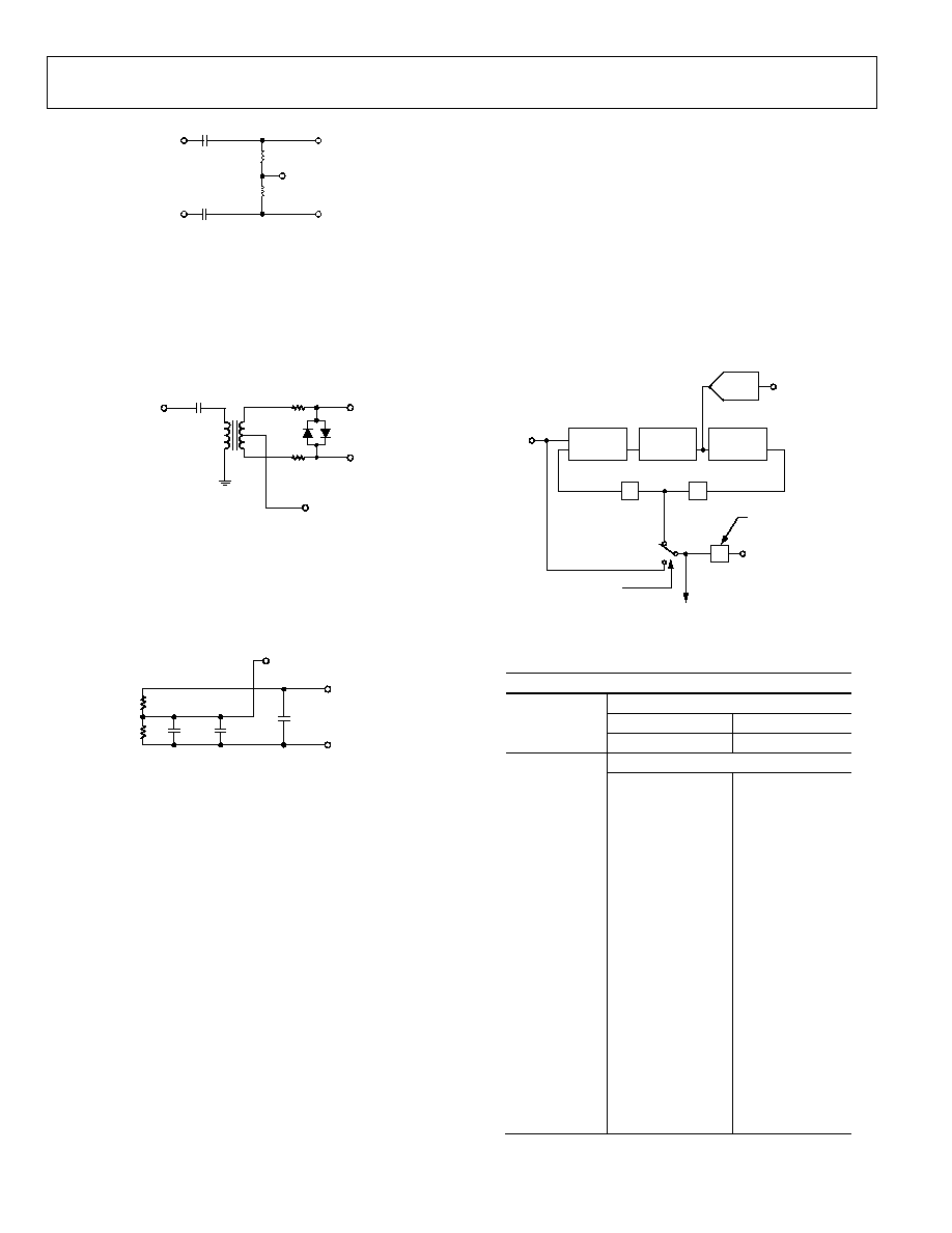
AD9776/AD9778/AD9779
Rev. 0 | Page 34 of 56
LVDS_P_IN
CLK+
50
50
0.1
F
0.1
F
LVDS_N_IN
CLK
V
CM
= 400mV
05361-068
Figure 68. LVDS DACCLK Drive Circuit
If a clean sine clock is available, it can be transformer-coupled
to DACCLK, as shown in Figure 68. Use of a CMOS or TTL
clock is also acceptable for lower sample rates. It can be routed
through a CMOS to LVDS translator, then ac-coupled, as
described in this section. Alternatively, it can be transformer-
coupled and clamped, as shown in Figure 69.
50
50
TTL OR CMOS
CLK INPUT
CLK+
CLK
V
CM
= 400mV
BAV99ZXCT
HIGH SPEED
DUAL DIODE
0.1
F
05361-069
Figure 69. TTL or CMOS DACCLK Drive Circuit
A simple bias network for generating VCM is shown in
Figure 70. It is important to use CVDD18 and CGND for the
clock bias circuit. Any noise or other signal that is coupled onto
the clock is multiplied by the DAC digital input signal and can
degrade the DAC's performance.
0.1
F
1nF
1nF
V
CM
= 400mV
CVDD18
CGND
1k
287
05361-070
Figure 70. DACCLK VCM Generator Circuit
Internal PLL Clock Multiplier/Clock Distribution
The internal clock structure on the devices allows the user to
drive the differential clock inputs with a clock at 1× or an
integer multiple of the input data rate or at the DAC output
sample rate. An internal PLL provides input clock multipli-
cation and provides all the internal clocks required for the
interpolation filters and data synchronization.
The internal clock architecture is shown in Figure 71. The
reference clock is the differential clock at Pins 5 and 6. This
clock input can be run differentially or singled-ended by
driving Pin 5 with a clock signal and biasing Pin 6 to the
midswing point of the signal at Pin 5. The clock architecture
can be run in the following configurations:
1.
PLL Enabled (Reg. 0x09, Bit 7 = 1). The PLL enable switch
shown in Figure 71 is connected to the junction of the N1
dividers (PLL VCO divide ratio) and N2 dividers (PLL
loop divide ratio). Divider N3 determines the interpo-
lation rate of the DAC, and the ratio N3/N2 determines the
ratio of reference clock/input data rate. The VCO runs
optimally over the range of 1.0 GHz to 2.0 GHz, so that N1
keeps the speed of the VCO within this range, although the
DAC sample rate can be lower. The loop filter components
are entirely internal and no external compensation is
necessary.
2.
PLL Disabled (Reg. 0x09, Bit 7 = 0). The PLL enable switch
shown in Figure 71 is connected to the reference clock
input. The differential reference clock input is the same as
the DAC output sample rate. N3 determines the
interpolation rate.
ADC
PHASE
DETECTION
VCO
DAC
INTERPOLATION
RATE
INTERNAL
LOOP
FILTER
0x0A (4:0)
LOOP FILTER
BANDWIDTH
REFERENCE CLOCK
(Pins 5 and 6)
0x0A (7:5)
PLL CONTROL
VOLTAGE RANGE
0x08 (7:2)
VCO RANGE
0x09 (7)
PLL ENABLE
INTERNAL DAC SAMPLE
RATE CLOCK
DATACLK OUT (Pin 37)
0x01 (7:6)
0x09 (6:5)
PLL VCO
DIVIDE RATIO
0x09 (4:3)
PLL LOOP
DIVIDE RATIO
÷
N
3
÷
N
2
÷
N
1
05361-
071
Figure 71. Internal Clock Architecture
Table 17. VCO Frequency Range vs. PLL Band Select Value
Typical PLL Lock Ranges
VCO Frequency Range in MHz
Typ at 25°C
Typ over Temp
PLL Band
Select
f
LOW
f
HIGH
f
LOW
f
HIGH
111111 (63)
Auto Mode
111110
(62) 2056 2170 2105 2138
111101
(61) 2002 2113 2048 2081
111100
(60) 1982 2093 2029 2061
111011
(59) 1964 2075 2010 2043
111010 58)
1947
2057
1992
2026
111001
(57) 1927 2037 1971 2006
111000
(56) 1907 2016 1951 1986
110111
(55) 1894 2003 1936 1972
110110
(54) 1872 1981 1913 1952
110101
(53) 1852 1960 1892 1931
110100
(52) 1841 1948 1881 1920
110011
(51) 1816 1923 1855 1895
110010
(50) 1796 1903 1835 1874
110001
(49) 1789 1895 1828 1867
110000
(48) 1764 1871 1803 1844
101111
(47) 1746 1853 1784 1826
101110
(46) 1738 1842 1776 1815
101101
(45) 1714 1820 1752 1794
101100
(44) 1700 1804 1737 1779
AD9776/AD9778/AD9779
Rev. 0 | Page 35 of 56
Typical PLL Lock Ranges
VCO Frequency Range in MHz
Typ at 25°C
Typ over Temp
PLL Band
Select
f
LOW
f
HIGH
f
LOW
f
HIGH
101011
(43) 1689 1790 1726 1764
101010
(42) 1657 1757 1695 1734
101001
(41) 1641 1738 1679 1714
101000
(40) 1610 1707 1649 1684
100111
(39) 1597 1689 1635 1666
100110
(38) 1568 1661 1607 1639
100101
(37) 1553 1641 1592 1617
100100
(36) 1525 1613 1562 1592
100011
(35) 1511 1595 1548 1572
100010
(34) 1484 1570 1519 1549
100001
(33) 1470 1552 1506 1528
100000
(32) 1441 1525 1474 1504
011111
(31) 1429 1509 1463 1487
011110
(30) 1403 1485 1433 1464
011101
(29) 1390 1469 1422 1447
011100
(28) 1362 1443 1391 1423
011011
(27) 1352 1429 1380 1407
011010
(26) 1325 1405 1352 1385
011001
(25) 1314 1390 1340 1369
011000
(24) 1290 1368 1315 1350
010111
(23) 1276 1351 1302 1332
010110
(22) 1253 1331 1277 1313
010101
(21) 1239 1313 1264 1295
010100
(20) 1183 1255 1205 1240
010011
(19) 1204 1275 1227 1259
010010
(18) 1151 1221 1172 1207
010001
(17) 1171 1240 1193 1224
010000
(16) 1148 1218 1170 1204
001111
(15) 1137 1204 1159 1189
001110
(14) 1116 1184 1137 1170
001101
(13) 1106 1171 1127 1157
001100
(12) 1086 1152 1106 1138
001011
(11) 1075 1138 1095 1124
001010
(10) 1055 1119 1075 1106
001001
(9) 1045 1107 1065 1093
001000
(8) 1027 1090 1047 1076
000111
(7) 1016 1076 1034 1062
000110 (6)
998
1059
1016
1046
000101 (5)
987
1046
1005
1032
000100 (4)
960
1017
977
1004
000011
(3) 933 989 949 976
000010
(2) 908 962 923 950
000001
(1) 883 936 898 925
000000
(0) 859 911 873 899
VCO Frequency Ranges
Because the PLL band covers greater than a 2× frequency range,
there can be two options for the PLL band select: one at the low
end of the range and one at the high end of the range. Under
these conditions, the VCO phase noise is optimal when the user
selects the band select value corresponding to the high end of
the frequency range. Figure 72 shows how the VCO bandwidth
and the optimal VCO frequency varies with the band select
value.
PLL Loop Filter Bandwidth
The loop filter bandwidth of the PLL is programmed via SPI
Reg. 0x0A, Bits <4:0>. Changing these values switches
capacitors on the internal loop filter. No external loop filter
components are required. This loop filter has a pole at 0 (P1),
and then a zero- (Z1) pole (P2) combination. Z1 and P2 occur
within a decade of each other. The location of the zero pole is
determined by Bit <4:0>. For a setting of 00000, the zero pole
occurs near 10 MHz. By setting Bits <4:0> to 11111, the Z1/P2
combination can be lowered to approximately 1 MHz. The
relationship between Bits <4:0> and the position of the zero
pole between 1 MHz and 10 MHz is linear. The internal compo-
nents are not low tolerance, however, and can drift by as much
as ±30%.
For optimal performance, the bandwidth adjustment
(Reg. 0x0A, Bits <4:0>) should be set to 11111 for all
operating modes with PLL enabled. The PLL bias settings
(Reg. 0x09, Bits <2:0>) should be set to 111. The PLL control
voltage (Reg. 0x0A, Bits <7:5>) is read back and is proportional
to the dc voltage at the internal loop filter output. With the PLL
bias settings given in this section, the readback from the PLL
control voltage should typically be 010 or possibly 001 or 011.
Anything outside of this range indicates that the PLL is not
operating correctly.
0
4
8
12
16
20
24
28
32
36
40
44
48
52
56
60
850
2150
2050
1950
1850
1750
1650
1450
1550
1350
1250
1150
1050
950
F
VCO
(MHz)
P
LL BAND
05361-072
Figure 72. Typical PLL Band Select vs. Frequency at 25°C
AD9776/AD9778/AD9779
Rev. 0 | Page 36 of 56
0
4
8
12
16
20
24
28
32
36
40
44
48
52
56
60
850
2150
2050
1950
1850
1750
1650
1450
1550
1350
1250
1150
1050
950
F
VCO
(MHz)
P
LL BAND
05361-113
Figure 73. Typical PLL Band Select vs. Frequency over Temperature
The AD977x has an autosearch feature that can be used to
determine the optimal settings for the PLL. To enable the
autosearch mode, set Reg. 0x08, Bits <7:2> to 11111b, and read
back the value from Reg. 0x08, Bits <7:2>. Autosearch mode is
intended to find the optimal PLL settings only, after which the
same settings should be applied in manual mode. It is not
recommended that the PLL be set to autosearch mode during
regular operation.
FULL-SCALE CURRENT GENERATION
Internal Reference
Full-scale current on the I DAC and Q DAC can be set from
8.66 mA to 31.66 mA. Initially, the 1.2 V band gap reference is
used to set up a current in an external resistor connected to
I120 (Pin 75). A simplified block diagram of the reference
circuitry is shown in Figure 74. The recommended value for the
external resistor is 10 k, which sets up an I
REFERENCE
in the
resistor of 120 A, which in turn provides a DAC output full-
scale current of 20 mA. Because the gain error is a linear
function of this resistor, a high precision resistor improves gain
matching to the internal matching specification of the devices.
Internal current mirrors provide a current-gain scaling, where
I DAC or Q DAC gain is a 10-bit word in the SPI port register
(Reg. 0x0A, 0x0B, 0x0E, and 0x0F). The default value for the
DAC gain registers gives an I
FS
of approximately 20 mA, where
I
FS
is equal to
32
DAC gain
1024
6
12
27
R
V
1.2
×
×
+
×
I DAC
DAC FULL-SCALE
REFERENCE
CURRENT
CURRENT
SCALING
I DAC GAIN
Q DAC GAIN
Q DAC
AD9779
VREF
10k
1.2V BAND GAP
0.1
F
I120
05361-073
Figure 74. Reference Circuitry
35
0
0
1000
DAC GAIN CODE
I
FS
(ma
)
30
25
20
15
10
5
200
400
600
800
05361-074
Figure 75. I
FS
vs. DAC Gain Code
Auxiliary DACS
Two auxiliary DACs are provided on the AD977x. The full-scale
output current on these DACs is derived from the 1.2 V band
gap reference and external resistor. The gain scale from the
reference amplifier current I
REFERENCE
to the auxiliary DAC refer-
ence current is 16.67 with the auxiliary DAC gain set to full
scale (10-bit values, SPI Reg. 0x0C, 0x0D, 0x10, and 0x11), this
gives a full-scale current of approximately 2 mA for auxiliary
DAC1 and auxiliary DAC2. The auxiliary DAC outputs are not
differential. Only one side of the auxiliary DAC (P or N) is
active at one time. The inactive side goes into a high impedance
state (>100 k). In addition, the P or N outputs can act as
current sources or sinks. The control of the P and N side
for both auxiliary DACs is via Reg. 0x0E and 0x10,
Bits <7:6>. When sourcing current, the output compliance
voltage is 0 V to 1.6 V; when sinking current, the output
compliance voltage is 0.8 V to 1.6 V.
The auxiliary DACs can be used for local oscillator (LO) cancel-
lation when the DAC output is followed by a quadrature modu-
lator. A typical DAC-to-quadrature modulator interface is shown
in Figure 76. Often, the input common-mode voltage for the
modulator is much higher than the output compliance range of
the DAC, so that ac coupling is necessary. If the required com-
mon-mode input voltage on the quadrature modulator matches
that of the DAC, then the ac coupling capacitors can be removed.
The input referred dc offset voltage of the quadrature modulator
(and the DAC output offset voltage mismatch) can result in LO
feedthrough on the modulator output, thus degrading system
performance. If the configuration of Figure 76 is used, the auxi-
liary DACs can be used to compensate for this dc offset, thus
reducing LO feedthrough. A low-pass or band-pass filter is
recommended when spurious signals from the DAC (distortion
and DAC images) at the quadrature modulator inputs can affect
the system performance. This filter should be placed at the
quadrature modulator inputs.

AD9776/AD9778/AD9779
Rev. 0 | Page 37 of 56
IDAC
IOUT1_P
AUX1_N
AUX1_P
IOUT1_N
AUX
DAC1
QUAD MOD
I INPUTS
QDAC
IOUT2_P
IOUT2_N
QUAD MOD
Q INPUTS
AUX2_N
AUX2_P
AUX
DAC2
05361-075
Figure 76. Typical Use of Auxiliary DACs
POWER DISSIPATION
Figure 77 to Figure 85 show the power dissipation of the 1.8 V
and 3.3 V digital and clock supplies in single DAC and dual
DAC modes. In addition to this, the power dissipation/current
of the 3.3 V supply (mode and speed independent) in single
DAC mode is 102 mW/31 mA. In dual DAC mode, this is
182 mW/51 mA.
0
0
250
f
DATA
(MSPS)
POW
ER
(
W
)
0.6
0.7
0.5
0.4
0.3
0.2
0.1
25
50
75
100
125
150
175
200
225
8
×
INTERPOLATION,
ZERO STUFFING
8
×
INTERPOLATION
4
×
INTERPOLATION
4
×
INTERPOLATION,
ZERO STUFFING
2
×
INTERPOLATION
1
×
INTERPOLATION
2
×
INTERPOLATION,
ZERO STUFFING
1
×
INTERPOLATION,
ZERO STUFFING
05361-076
Figure 77. Power Dissipation, I Data Only, Single DAC Mode
0
0
250
f
DATA
(MSPS)
POW
ER
(
W
)
0.6
0.7
0.5
0.4
0.3
0.2
0.1
25
50
75
100
125
150
175
200
225
8
×
INTERPOLATION,
ZERO STUFFING
4
×
INTERPOLATION,
ZERO STUFFING
1
×
INTERPOLATION
2
×
INTERPOLATION,
ZERO STUFFING
1
×
INTERPOLATION,
ZERO STUFFING
05361-077
8
×
INTERPOLATION,
f
DAC
/4,
f
DAC
/2
,
f
DAC
/8
,
MODULATION OFF
4
×
INTERPOLATION,
f
DAC
/4,
f
DAC
/2
,
MODULATION OFF
2
×
INTERPOLATION,
f
DAC
/2,
MODULATION OFF
Figure 78. Power Dissipation, Dual DAC Mode
0
0
250
f
DATA
(MSPS)
POW
ER
(
W
)
0.4
25
50
75
100
125
150
175
200
225
8
×
INTERPOLATION
4
×
INTERPOLATION
2
×
INTERPOLATION
1
×
INTERPOLATION
0.3
0.2
0.1
05361-078
Figure 79. Power Dissipation, Digital 1.8 V Supply, I Data Only, Real Mode,
Does Not Include Zero Stuffing
0
0
250
f
DATA
(MSPS)
POW
ER
(
W
)
0.08
25
50
75
100
125
150
175
200
225
8
×
INTERPOLATION
4
×
INTERPOLATION
2
×
INTERPOLATION
1
×
INTERPOLATION
0.06
0.04
0.02
05361-079
Figure 80. Power Dissipation, Clock 1.8 V Supply, I Data Only, Real Mode,
Includes Modulation Modes, Does Not Include Zero Stuffing

AD9776/AD9778/AD9779
Rev. 0 | Page 38 of 56
0
0
250
f
DATA
(MSPS)
POW
ER
(
W
)
0.075
25
50
75
100
125
150
175
200
225
0.050
0.025
ALL INTERPOLATION MODES
05361-080
Figure 81. Digital 3.3 V Supply, I Data Only, Real Mode, Includes Modulation
Modes and Zero Stuffing
0
0
250
f
DATA
(MSPS)
POW
ER
(
W
)
0.8
0.7
0.6
0.5
0.4
0.3
0.2
0.1
25
50
75
100
125
150
175
200
225
2
×
INTERPOLATION
4
×
INTERPOLATION
1
×
INTERPOLATION,
NO MODULATION
8
×
INTERPOLATION, f
DAC
/8,
f
DAC
/4,
f
DAC
/2,
NO MODULATION
05361-081
Figure 82. Power Dissipation, Digital 1.8 V Supply, I and Q Data, Dual DAC
Mode, Does Not Include Zero Stuffing
0
0
250
f
DATA
(MSPS)
POW
ER
(
W
)
0.125
25
50
75
100
125
150
175
200
225
2
×
INTERPOLATION
4
×
INTERPOLATION
1
×
INTERPOLATION,
NO MODULATION
8
×
INTERPOLATION, f
DAC
/8,
f
DAC
/4,
f
DAC
/2,
NO MODULATION
0.100
0.075
0.050
0.025
05361-082
Figure 83. Power Dissipation, Clock 1.8 V Supply, I and Q Data, Dual DAC
Mode, Does Not Include Zero Stuffing
0
0
250
f
DATA
(MSPS)
POW
ER
(
W
)
0.075
25
50
75
100
125
150
175
200
225
0.050
0.025
ALL INTERPOLATION MODES
05361-083
Figure 84. Digital 3.3 V Supply, I and Q Data, Dual DAC Mode
0.16
0
0
1200
f
DAC
(MSPS)
POW
ER
(
W
)
0.14
0.12
0.10
0.08
0.06
0.04
0.02
200
400
600
800
1000
05361-084
Figure 85. Power Dissipation of Inverse Sinc Filter
POWER-DOWN AND SLEEP MODES
The AD977x has a variety of power-down modes, so that the
digital engine, main TxDACs, or auxiliary DACs can be
powered down individually or together. Via the SPI port, the
main TxDACs can be placed in sleep or power-down mode. In
sleep mode, the TxDAC output is turned off, thus reducing
power dissipation. The reference remains powered on, however,
so that recovery from sleep mode is very fast. With the power-
down mode bit set (Reg. 0x00, Bit 4), all analog and digital
circuitry, including the reference, is powered down. The SPI
port remains active in this mode. This mode offers more
substantial power savings than sleep mode, but the turn on
time is much longer. The auxiliary DACs also have the
capability to be programmed into sleep mode via the SPI port.

AD9776/AD9778/AD9779
Rev. 0 | Page 39 of 56
INTERLEAVED
INPUT DATA
TxENABLE CAN REMAIN
HIGH OR TOGGLE FOR
I/Q SYNCHRONIZATION
I1
Q1
I2
Q2
TxENABLE
FLUSHING
INTERPOLATION
FILTERS
POWER
DOWN DIGITAL
SECTION
05361-
085
The auto power-down enable bit (Reg. 0x00, Bit 3) controls the
power-down function for the digital section of the devices. The
auto power-down function works in conjunction with the
TXENABLE pin (Pin 39) according to the following:
TXENABLE (Pin 39) =
0: autopower-down enable =
0: Flush data path with 0s
1: Flush data for multiple DACCLK cycles; then
automatically place the digital engine in power-down
state. DACs, reference, and SPI port are not affected.
Figure 86. TxEnable Function
The TxEnable function can be inverted by changing the status
of Reg. 0x02, Bit 1. The other bit that controls IQ ordering is the
Q-first bit (Reg. 0x02, Bit 0). With the Q-first bit reset to the
default of 0, the IQ pairing that is latched is the I1Q1, I2Q2, etc.
With IQ first set to 1, the first I data is discarded and the pairing
is I2Q1, I3Q2, etc. Note that with IQ-first set, the I data is still
routed to the internal I channel, the Q data is routed to the
internal Q channel, and only the pairing changes.
or TXENABLE (Pin 39) =
1: Normal operation
If the TxEnable invert bit (Reg. 0x02, Bit 1) is set, the function
of this TXENABLE pin is inverted.
INTERLEAVED DATA MODE
TIMING INFORMATION
The TxEnable bit is dual function. In dual port mode, it is
simply used to power down the digital section of the devices. In
interleaved mode, the IQ data stream is synchronized to
TxEnable. Therefore, to achieve IQ synchronization, TxEnable
should be held low until an I data word is present at the inputs
to Data Port 1. If a DATACLK rising edge occurs while
TxEnable is at a high logic level, IQ data becomes synchronized
to the DATACLK output. TxEnable can remain high and
the input IQ data remains synchronized. To be backwards-
compatible with previous DACs from ADI, such as the AD9777
and AD9786, the user can also toggle TxEnable once during
each data input cycle, thus continually updating the synchroni-
zation. If TxEnable is brought low and held low for multiple
DACCLK cycles, then the devices flush the data in the interpo-
lation filters, and shut down the digital engine after the filters
are flushed. The amount of DACCLK cycles it takes to go into
this power-down mode is then a function of the length of the
equivalent 2×, 4×, or 8× interpolation filter. The timing of
TxEnable, I/Q select, filter flush, and digital power-down are
shown in Figure 86.
Figure 87 to Figure 89 show some of the various timing
possibilities when the PLL is enabled. The combination of the
settings of N2 and N3 means that the reference clock frequency
can be a multiple of the actual input data rate. Figure 87 to
Figure 89 show, respectively, what the timing looks like when
N2/N3 = 1 and 2.
In interleaved mode, set-up and hold times of DATACLK out to
data in are the same as those shown in Figure 87 to Figure 89. It
is recommended that any toggling of TxEnable occurs concur-
rently with the digital data input updating. In this way, timing
margins between DATACLK, TxEnable, and digital input data
are optimized.
Figure 89 shows the timing specifications when PLL is disabled.
The reference clock is at the DAC output sample rate. In the
example shown in Figure 89, if PLL is disabled, the interpola-
tion is 4×. The set-up and hold time for the input data are with
respect to the rising edge of DATACLK out. Note that if
Reg. 0x02, Bit 2 is set, DATACLK out is inverted so the latching
clock edge becomes DATACLK out falling edge.
t
S
t
D
t
H
REFERENCE CLOCK
DATACLK OUT
INPUT DATA
05361-086
Figure 87. Timing Specifications, PLL Enabled, Reference Clock = 1× Input Sample Rate
1

AD9776/AD9778/AD9779
Rev. 0 | Page 40 of 56
t
S
t
D
t
H
REFERENCE CLOCK
DATACLK OUT
INPUT DATA
05361-087
Figure 88. Timing Specifications, PLL Enabled, Reference Clock = 2× Input Sample Rate
1
t
S
t
D
t
H
REFERENCE CLOCK
DATACLK OUT
t
S
= 3ns MIN
t
H
= 0.78ns MIN
t
D
= 5.0ns TYP
(DATACLK DELAY DISABLED)
INPUT DATA
05361-088
Figure 89. Timing Specifications, PLL Disabled, 4× Interpolation
1
For an in-depth description of how TxDAC timing specifications are specified, please read Analog Devices, application note AN748, "Set-up and Hold Measurements in
High Speed CMOS Input DACs."
Using Data Delay to Meet Timing Requirements
To meet strict timing requirements at input data rates of up to
250 MSPS, the AD977x has a fine timing feature. Fine timing
adjustments can be made by programming values into the data
clock delay register (Reg. 0x04, Bit <7:4>). This register can be
used to add delay between the DACCLK in and the DATACLK
out. Figure 90 shows the default delay present when DATACLK
delay is disabled. The disable function bit is found in Reg. 0x02,
Bit 4. Figure 91 shows the delay present when DATACLK delay
is enabled and set to 0000. Figure 92 indicates the delay when
DATACLK delay is enabled and set to 1111. Note that the set-up
and hold times specified for data to DATACLK are defined for
DATACLK delay disabled.
CH1 1.00V
TEK RUN: 5.00GS/s
SAMPLE
CH2
500mV
M2.00ns
CH1 420mV
: 4.48nS
@: 40.28nS
2
1
05361-089
Figure 90. Delay from DACCLK to DATACLK with DATACLK Delay Disabled
CH1 1.00V
TEK RUN: 5.00GS/s
SAMPLE
CH2
500mV
M2.00ns
CH1 420mV
: 4.76nS
@: 35.52nS
2
1
05361-090
Figure 91. Delay from DACCLK to DATACLK Out with DATACLK Delay = 0000
CH1 1.00V
TEK RUN: 5.00GS/s
SAMPLE
CH2
500mV
M2.00ns
CH1 420mV
: 7.84nS
@: 32.44nS
2
1
05361-091
Figure 92. Delay from DACCLK to DATACLK Out with DATACLK Delay = 1111
AD9776/AD9778/AD9779
Rev. 0 | Page 41 of 56
The difference between the minimum delay shown in Figure 91
and the maximum delay shown in Figure 92 is the range
programmable via the DATACLK delay register. The delay
(in absolute time) when programming DATACLK delay
between 0000 and 1111 is a linear extrapolation between these
two figures. The typical delays per increment over temperature
are shown in Table 18.
Table 18. Data Delay Line Typical Delays Over Temperature
Delays
40°C +25°C +85°C Unit
Delay Between Disabled and
Enabled
370 416 432 ps
Average Delay per Increment
171 183 197 ps
The frequency of DATACLK out depends on several program-
mable settings. Interpolation, zero stuffing, and interleaved/
dual port mode all have an effect on the DACCLK frequency.
The divisor function between DACCLK and DATACLK is equal
to the values shown in Table 19.
Table 19.
Interpolation
Zero Stuffing
Input Mode
Divisor
1 Disabled
Dual
port
1
2 Disabled
Dual
port
2
4 Disabled
Dual
port
4
8 Disabled
Dual
port
8
1 Disabled
Interleaved
invalid
2 Disabled
Interleaved
1
4 Disabled
Interleaved
2
8 Disabled
Interleaved
4
1 Enabled
Dual
port
2
2 Enabled
Dual
port
4
4 Enabled
Dual
port
8
8 Enabled
Dual
port
16
1 Enabled
Interleaved
1
2 Enabled
Interleaved
2
4 Enabled
Interleaved
4
8 Enabled
Interleaved
8
In addition to this divisor function, DATACLK can be divided
by up to an additional factor of 4, according to the state of the
DATACLK divide register (Reg. 0x03, Bit <5:4>) (see Table 20).
Table 20.
Reg. 0x03, Bit <5:4>
Divider Ratio
00 1
01 2
10 4
11 1
The maximum divisor resulting from the combination of the
values in Table 19, and the DATACLK divide register is 32.
Manual Input Timing Correction
Correction of input timing can be achieved manually. The
correction function is controlled by Reg. 0x03, Bits <7:6>. The
function is programmed as shown in Table 21.
Table 21.
Reg. 0x03, Bits <7:6>
Function
00
Error check disabled
01 Reserved
10 Reserved
11 Reserved
Necessary corrections can be made by adjusting DATACLK
delay and the DATACLK invert bit (Reg. 2, Bit 2). When doing
initial timing verification, the user should set input data timing
error tolerance (Reg. 0x03, Bit <3:0>) to 1111. DATACLK delay
can then be swept to find the range over which the timing is
valid. The final value for data delay should be the value that
corresponds to the middle of the valid timing range. If a valid
timing range is not found during this sweep, the user should
invert the DATACLK invert bit and repeat the process. If a valid
timing window is still not found, then the input data timing
error tolerance should be decremented by 1, and the procedure
should be repeated.
Multi-DAC Synchronization
Sync Pulse Generation (Master Devices)
In applications where multiple devices are used and need to be
synchronized, the AD977x provides a flexible synchronization
engine. There are two options for multi-DAC synchronization.
In the first situation, one device can be used as a master and the
rest of the devices can be used as slaves. The second option is
that all devices operate as slaves. Both operations have the same
timing restrict-ions and there are no performance tradeoffs for
either mode. The following text describes the master mode. The
differential input clock drives the master device and the master
in turn generates SYNC_O+ and SYNC_O. These two signals
use LVDS levels to generate a differential synchronization
signal, which in turn is used to synchronize all the slave devices.
SYNC_O+ and SYNC_O must loop back to the sync inputs
(SYNC_I+ and SYNC_I) of the master for multiple device
synchronization. The master mode is enabled by writing the
sync driver enable bit (Reg. 0x07, Bit 6) to a Logic 1. The
SYNC_O signal speed can be an integer divisor of the DACCLK
speed, according to Reg. 0x04, Bits <3:1>. Enabling a device in
slave mode is accomplished by writing the sync receiver enable
bit (Reg. 0x07, Bit 7) to a Logic 1. The timing of the DAC input
clock and the sync output signals on the master device are
shown in Figure 93.

AD9776/AD9778/AD9779
Rev. 0 | Page 42 of 56
DACCLK
SYNC OUT DELAY
0x04 (0); 0x05 (7:4)
(~180ps/increment)
SYNC OUT DIVISOR IS CONTROLLED BY:
0x04 (3:1)
000
f
DAC
/32
001
f
DAC
/16
010
f
DAC
/8
011
f
DAC
/4
100
f
DAC
/2
101
f
DAC
/1
110 UNDEFINED
111 UNDEFINED
SYNC TRIGGERING EDGE
0x07 (5)
1RISING EDGE
0FALLING EDGE
LVDS DAC
SYNC OUT (/1)
LVDS DAC
SYNC OUT (/4)
LVDS DAC
SYNC OUT (/16)
05361-092
Figure 93. DACCLK/Sync Output Timing
The sync output pulse must then be distributed from the master
to all the slave devices. This might require that the user imple-
ment circuitry outside of the device that splits the LVDS signal.
The splitter delivers the SYNC_O signal from the master to the
multiple slave device SYNC_I pins. A block diagram of this
implementation is shown in Figure 94. The equalization from
the CLK source and SYNC_O to the DACCLK and sync inputs
of the multiple AD977x devices is critical. For the multichip
synchronization to operate correctly at maximum specified
DAC sample rates, the DACCLK inputs must be phase aligned
to ±100 ps. The SYNC_I inputs must also be phase aligned to
±100 ps. At lower DAC sample rates, this timing alignment can
be relaxed.
MASTER
DAC
LVDS DRIVER AND DELAY
EQUALIZATION
EQUALIZATION
CLOCK
SOURCE
SYNC IN
SYNC OUT
DACCLK
SLAVE
DAC
SYNC IN
DACCLK
SLAVE
DAC
SYNC IN
DACCLK
05361-093
Figure 94. Implementation of Sync Signal Distribution in Master/Slave Mode
SLAVE
DAC
EQUALIZATION/FREQUENCY DIVISION
EQUALIZATION
CLOCK
SOURCE
SYNC_IN
DACCLK
SLAVE
DAC
SYNC_IN
DACCLK
SLAVE
DAC
SYNC_IN
DACCLK
05361-094
Figure 95. Implementation of Sync Signal Distribution in Slave Mode
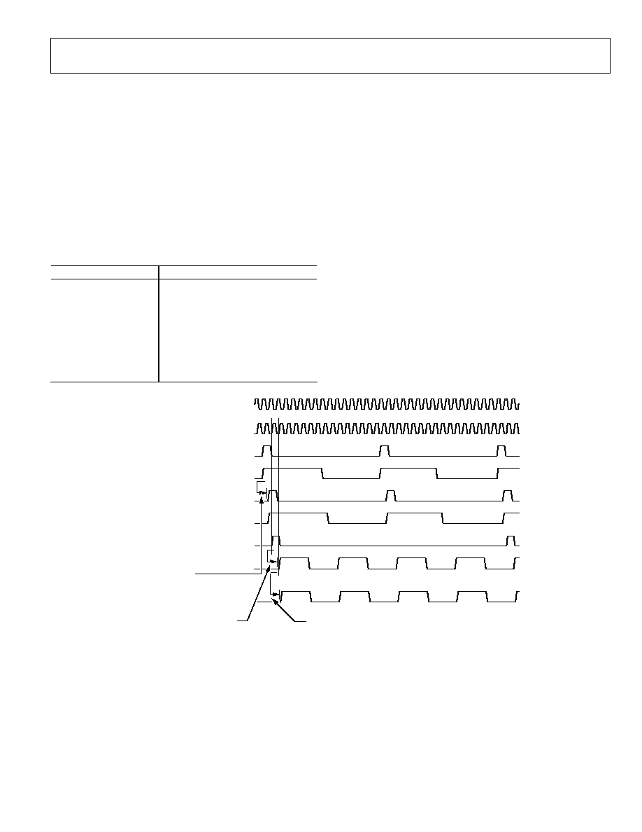
AD9776/AD9778/AD9779
Rev. 0 | Page 43 of 56
Internal Synchronization in Slave Devices
Sync Pulse Receiver (Slave Devices)
The internal timing functions in the slave device are shown in
Figure 96. The duty cycle of the SYNC_I signal is not restricted
to 50%. The minimum restriction on duty cycle for SYNC_I is
that it stays high for at least one full DACCLK cycle. Figure 96
shows two possible SYNC_I signals: one with a 50% duty cycle
and another one with a minimum duty cycle. More details on
SYNC_I timing restriction are given in the SYNC_I Timing
Restrictions section.
The following description of SYNC_I on the slave devices also
applies to the SYNC_I on the master device. The timing for
SYNC_I on the master must match that of the slave devices.
The SYNC_I pulses, referred to in Figure 94 and shown in more
detail in Figure 96 are not restricted by their duty cycle. The
only restriction is that each sync pulse remains high for at least
one DACCLK cycle. However, the slave DAC receiving the sync
pulse must know the speed of the input sync pulse.
DACCLK samples SYNC_I and generates the internal sync signal
(SYNC_I_int). The period of SYNC_I_int is always DACCLK/32.
If the rate of SYNC_I is greater than DACCLK/32, the extra
pulses are stripped off. Figure 96 shows that the SYNC_I period
= DACCLK/16, so that every other SYNC_I pulse is stripped.
DACCLK_SMP is an internal signal, equal in frequency to the
DACCLK/interpolation rate. DACCLK_SMP is synthesized by
DACCLK, but synchronized by SYNC_I. Note that there is also
a programmable delay (sync input delay) between SYNC_I_int
and DACCLK_SMP. This programmable delay adds even more
flexibility to the timing interface. Figure 96 shows that the
interpolation is set to 8× (DACCLK_SMP rate is 1/8 that of
DACCLK).
The ratio of DACCLK to the SYNC_I speed is determined by
the values of the input sync pulse frequency (Reg. 0x05,
Bits <3:1>), as shown in Table 22.
Table 22.
Reg. 0x05, Bits <3:1>
Divider Ratio
000 DACCLK/32
(default)
001 DACCLK/16
010 DACCLK/8
011 DACCLK/4
100 DACCLK/2
101 Undefined
110 Undefined
111 Undefined
DACCLK_ext
DACCLK_int
(Prop, Delay)
DCLK_SMP
DCLK_OUT
SYNC_I_ext_min_dutycycle
SYNC_I_ext_50%dutycycle
SYNC_I_int (Post SYNC DELAY)
SYNC_I_int (Post SYNC DELAY)
SYNC_stripped (Post Edge Detector)
DATA CLOCK DELAY
0x04 (7:4)
DATA CLOCK OFFSET
0x07 (4:0)
(1 DACCLK cycle/increment)
SYNC INPUT DELAY
0x06 (7:4)
(~100ps/increment)
05361-095
Figure 96. Internal and External Timing for Master or Slave Device

AD9776/AD9778/AD9779
Rev. 0 | Page 44 of 56
FF1
PROGRAMMABLE
DELAY
SYNC
INPUT
DELAY
0x05 (0), 0x06 (7:4)
EDGE DETECTOR, DETECTS
ON ONE OUT OF EVERY
32 DACCLK EDGES
DACCLK
(Internal
Delayed)
LVDS DIFFERENTIAL
SYNC INPUT
D
REGISTERED
SYNC_I_int
0x06 (3:0)
Q
PROGRAMMABLE
DELAY
FF2
D
CLK
Q
FF3
D
CLK
Q
IRQ, 0x19 (6)
IRQ ENABLE, 0x19 (2)
05361-096
Figure 97. Simplified Internal Synchronization Logic
SYNC_I Timing Restrictions
The AD977x can register timing errors for the SYNC_I signals.
The block diagram for this synchronization logic is shown in
Figure 94, which is very similar to the data input synchro-
nization circuit shown in Figure 95. The difference is that the
circuit shown in Figure 95 uses the DACCLK to properly
register SYNC_I. The delay is programmable by Reg. 0x06, Bits
<3:0>. IRQ is registered in Reg. 0x19, Bit 6.
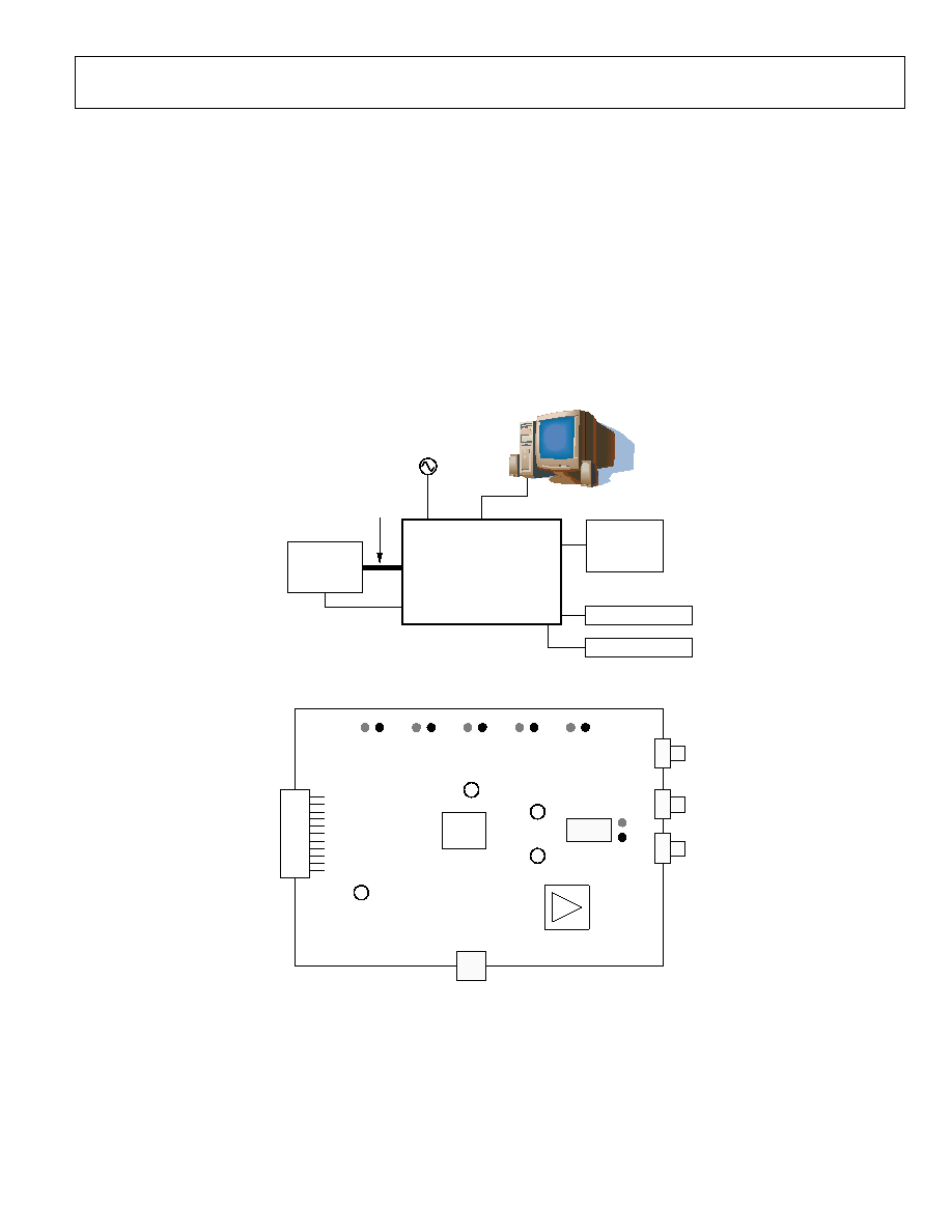
AD9776/AD9778/AD9779
Rev. 0 | Page 45 of 56
EVALUATION BOARD OPERATION
The AD977x evaluation board is designed to optimize the DAC
performance and the speed of the digital interface while
remaining user friendly. To operate the board, the user needs a
power source, a clock source, and a digital data source. The user
also needs a spectrum analyzer or an oscilloscope to look at the
DAC output. The diagram in Figure 98 illustrates the test setup.
A sine or square wave clock works well as a clock source. The dc
offset on the clock is not a problem, since the clock is ac-
coupled on the evaluation board before the DACCLK inputs.
All necessary connections to the evaluation board are shown in
more detail in Figure 99.
The evaluation board comes with software that allows the user
to program the SPI port. Via the SPI port, the devices can be
programmed into any of its various operating modes. When
first operating the evaluation board, it is useful to start with a
simple configuration, that is, a configuration in which the SPI
port settings are as close as possible to the default settings. The
default software window is shown in Figure 100. The arrows
indicate which settings need to be changed for an easy first time
evaluation. Note that this implies that the PLL is not being used
and that the clock being used is at the speed of the DAC output
sample rate. For a more detailed description of how to use the
PLL, see the PLL Loop Filter Bandwidth section.
DIGITAL
PATTERN
GENERATOR
ADAPTER
CABLES
CLOCK
GENERATOR
AD9779
EVALUATION
BOARD
CLKIN
SPI PORT
DATACLK OUT
CLOCK IN
SPECTRUM
ANALYZER
1.8V POWER SUPPLY
3.3V POWER SUPPLY
05361-097
Figure 98. Typical Test Setup
SPI PORT
AD9779
J1 CLOCK IN
P4 Digital Input Connector
S7 DCLKOUT
AUX33
DVDD18
DVDD33
CVDD18
AVDD33
J2
5V Supply
ANALOG
DEVICES
AD9779/8/6
REV D
S5 OUTPUT 1
S6 OUTPUT 2
AD8349
LOCAL OSC
INPUT
MODULATOR
OUTPUT
+5V
GND
JP4
JP15
JP8
JP14
JP3
JP16
JP2
JP17
05361-098
Figure 99. AD977x Evaluation Board Showing all Connections

AD9776/AD9778/AD9779
Rev. 0 | Page 46 of 56
1. SET INTEROPOLATION RATE
2. SET INTEROPOLATION FILTER MODE
3. SET INPUT DATA FORMAT
4. SET DATACLK POLARITY TO MATCH INPUT TIMING
05361-099
Figure 100. SPI Port Software Window
The default settings for the evaluation board allow the user to
view the differential outputs through a transformer that
converts the DAC output signal to a single-ended signal. On the
evaluation board, these transformers are designated T1A, T2A,
T3A, and T4A. There are also four common-mode transformers
on the board that are designated T1B, T2B, T3B, and T4B. The
recommended operating setup is to place the transformer and
common-mode transformer in series. A pair of transformers
and common-mode transformers are installed on each DAC
output, so that the pairs can be set up in either order. As an
example, for the frequency range of dc to 30 MHz, it is
recommended that the transformer is placed right after the
DAC. Above DAC output frequencies of 30 MHz, it is
recommended that the common-mode transformer is placed
right after the DAC outputs, followed by the transformer.
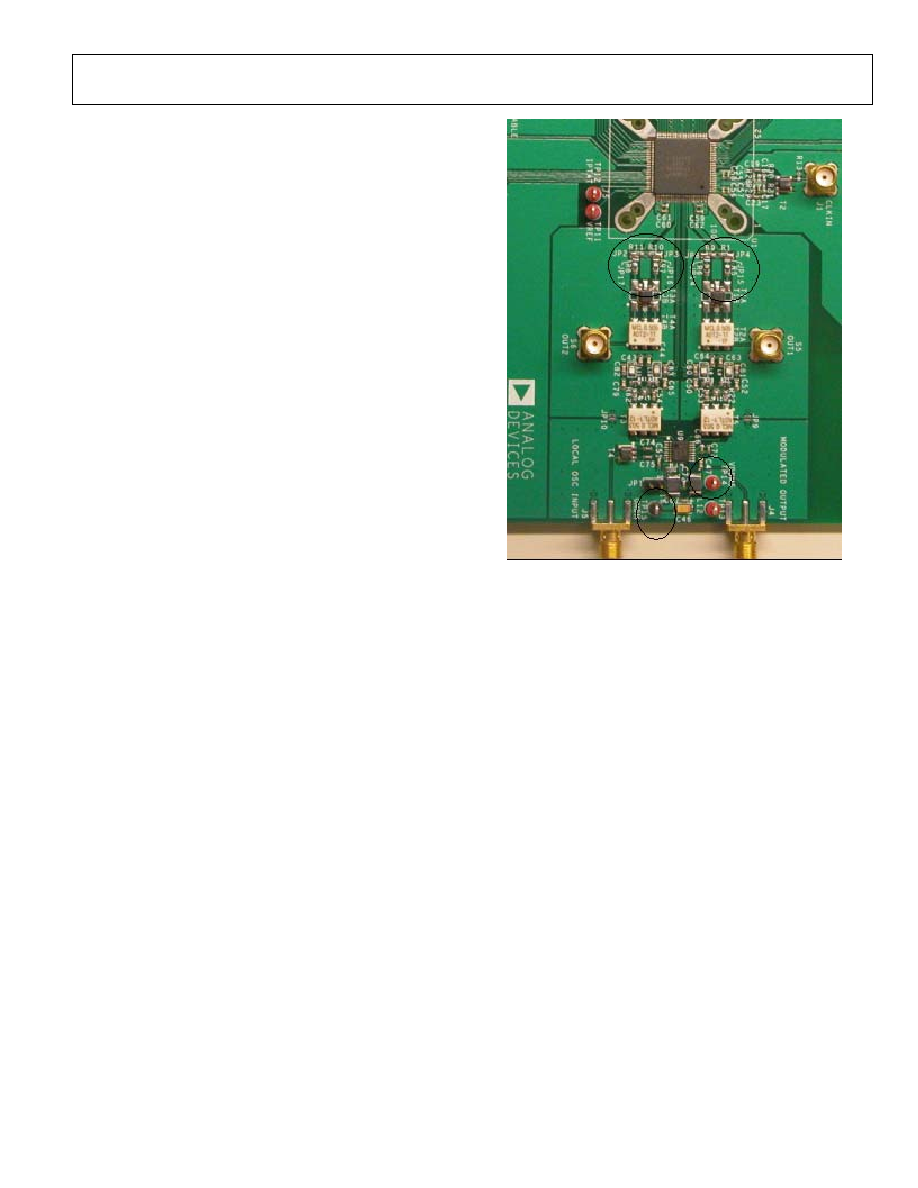
AD9776/AD9778/AD9779
Rev. 0 | Page 47 of 56
MODIFYING THE EVALUATION BOARD TO USE
THE AD8349 ON-BOARD QUADRATURE
MODULATOR
The evaluation board contains an Analog Devices AD8349
quadrature modulator. The AD977x and AD8349 provide an
easy-to-interface DAC/modulator combination that can be
easily evaluated on the evaluation board. To route the DAC
output signal to the quadrature modulator, the following
jumper settings must be made:
Unsoldered: JP14, JP15, JP16, JP17
Soldered: JP2, JP3, JP4, JP8
The DAC output area of the evaluation board is shown in
Figure 101. The jumpers that need to be changed to use the
AD8349 are circled. Also circled are the 5 V and GND
connections for the AD8349.
05361-100
Figure 101. Photo of Evaluation Board, DAC Output Area
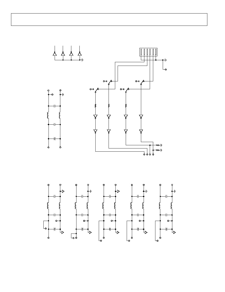
AD9776/AD9778/AD9779
Rev. 0 | Page 48 of 56
EVALUATION BOARD SCHEMATICS
C6
9
0.1
F
+
CV
DD1
8
TP2 BLACK
TP17 RE
D
TP1 RE
D
L1
EXC
-
C
L4532U
1
L6
EXC
-
C
L4532U
1
C6
8
0.1
F
C7
7
22
F
16V
C
V
D
D
18_IN
C6
6
0.1
F
+
V
DDM
DGND2
2
TP14 RE
D
TP15 BLACK
L12
EXC
-
C
L4532U
1
L16
EXC
-
C
L4532U
1
C6
7
0.1
F
C4
6
22
F
16V
V
DDM_
I
N
DGND2
TP13 RE
D
R5
1
9k
R5
2
10k
R5
5
10k
C2
6
0.1
F
+
AV
DD3
3
TP8 BLACK
TP19 RE
D
TP5 RE
D
L3
EXC
-
C
L4532U
1
L13
EXC
-
C
L4532U
1
C2
8
0.1
F
C2
0
22
F
16V
A
V
D
D
33_IN
C4
9
0.1
F
+
DP
WR3
3
TP10 BLACK
TP21 RE
D
TP7 RE
D
L5
EXC
-
C
L4532U
1
L15
EXC
-
C
L4532U
1
C4
8
0.1
F
C2
2
22
F
16V
D
P
W
R
33_IN
+
C7
0
0.1
F
DV
DD1
8
TP4 BLACK
TP18 RE
D
TP3 RE
D
L2
EXC
-
C
L4532U
1
L7
EXC
-
C
L4532U
1
C7
1
0.1
F
C7
6
22
F
16V
D
V
D
D
18_IN
C4
2
0.1
F
+
DV
DD3
3
TP9 BLACK
TP20 RE
D
TP6 RE
D
L4
EXC
-
C
L4532U
1
L14
EXC
-
C
L4532U
1
C4
5
0.1
F
C2
1
22
F
16V
D
V
D
D
33_IN
3
U6
4
7
4
AC1
4
11
U6
10
7
4
AC1
4
9
U6
8
7
4
AC1
4
5
U6
6
7
4
AC1
4
2
U5
CS
B
S1
SW
SEC
M
A
S3
SW
SEC
M
A
S2
SW
SEC
M
A
1
1
3
2
7
4
AC1
4
SPI_C
SB
SPI_C
LK
SPI_SD
I
SPI_SD
O
4
U5
3
7
4
AC1
4
6
U5
5
7
4
AC1
4
1
U6
2
7
4
AC1
4
12
U5
13
7
4
AC1
4
10
U5
11
7
4
AC1
4
8
U5
9
7
4
AC1
4
13
U6
12
7
4
AC1
4
P1
1
2
3
4
5
6
R5
3
9k
R5
4
9k
SD
I
1
3
2
SC
LK
1
3
2
S4
SW
SEC
M
A
TP16 RE
D
TJ
AK0
6
RAP
CLAS
S
= IO
FC
I-
68898
SD
O
1
3
2
05361-101
Figure 102. Evaluation Board, Rev. D, Power Supply Decoupling and SPI Interface
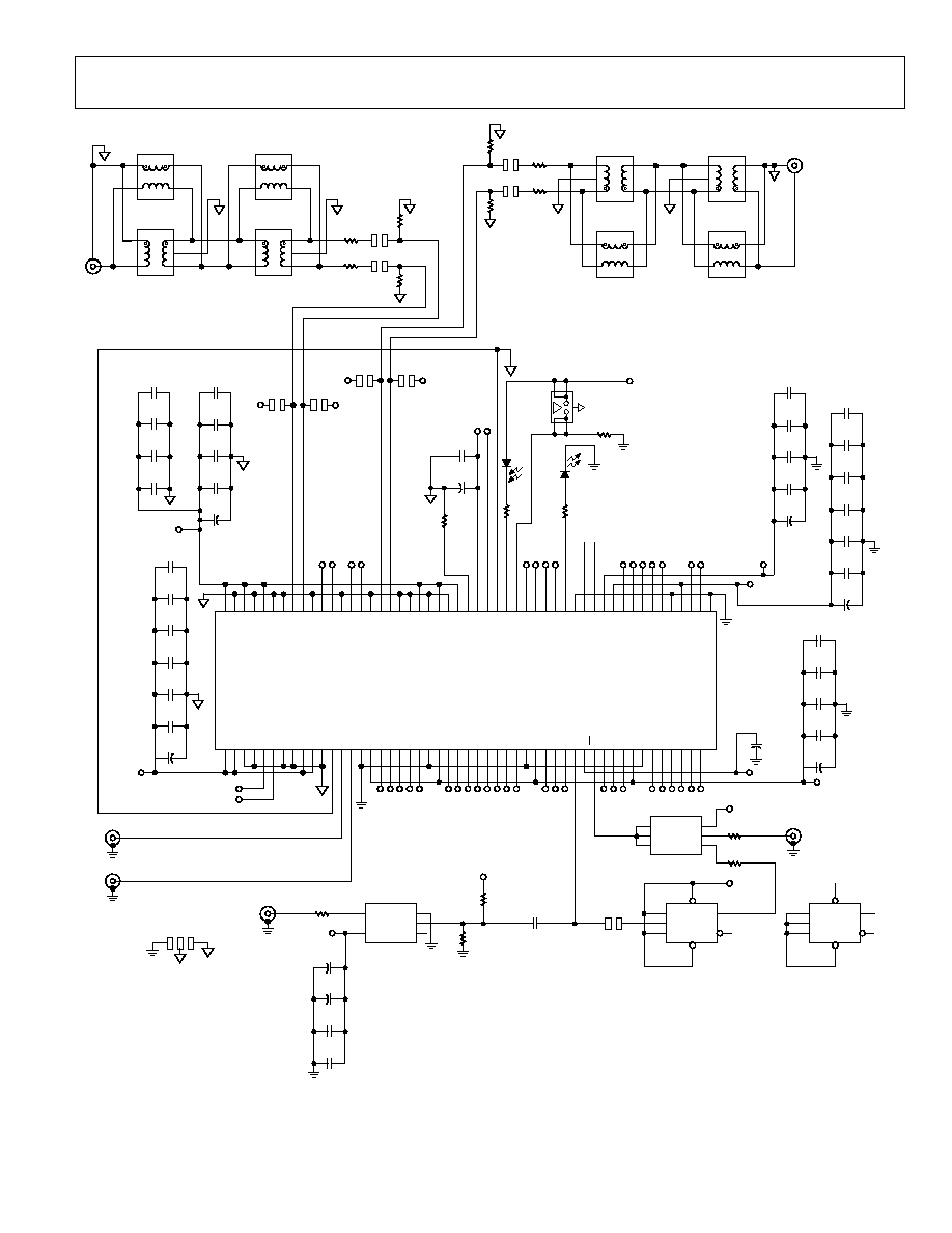
AD9776/AD9778/AD9779
Rev. 0 | Page 49 of 56
6
AUX
1
_
P
AUX
1
_
N
AUX
2
_
N
CLK_
N
CLK_
P
DCLK
I
120
I
O
U
T
1_N
I
O
U
T
1_P
I
O
U
T
1_N
I
O
U
T
1_P
I
O
U
T
2_N
I
O
U
T
2_P
I
O
U
T
2_N
I
O
U
T
2_P
IP
TAT
IRQ
P1D
0
P1D
1
P1D
10
P1D
11
P1D
12
P1D
13
P1D
14
P1D
15
P1D
2
P1D
3
P1D
4
P1D
5
P1D
6
TP
1
2
RE
D
P1D
7
P1D
8
P1D
9
P2D
0
P2D
1
P2D
10
P2D
11
P2D
12
P2D
13
P2D
14
P2D
15
P2D
2
P2D
3
P2D
4
P2D
5
P2D
6
P2D
0
P2D
1
P2D
2
P2D
3
P2D
4
P2D
5
P2D
6
P2D
7
JP7
JP18
U11
U1
9779TQ
F
P
+ C4
4.7
F
C29
1nF
VOLT
DVDD33
DVDD18
P2D
8
P2D
9
PA
D
P
LL_
LO
CK
R
ESET
SPI
_C
L
K
SPI
_C
SB
SPI
_SD
I
SPI
_SD
O
SPI
_C
L
K
SPI
_C
SB
SPI
_SD
I
SPI
_SD
O
SYN
C
_1N
SYN
C
_1P
S
Y
NC_
O
N
S
Y
NC_
O
P
VD
D
18_43
VD
D
A
33_76
VD
D
A
33_78
VD
D
A
33_80
VD
D
C
18_1
VD
D
C
18_10
VD
D
C
18_2
VD
D
C
18_9
VD
D
D
18_23
VD
D
D
18_33
VD
D
D
18_53
VD
D
D
18_60
V
DDD1
8
VD
D
D
33_38
VD
D
D
33_61
VR
EF
_74
VSSA
_77
VSSA
_79
VSSA
_81
VSSA
_82
VSSA
_85
VSSA
_88
VSSA
_91
VSSA
_94
VSSA
_95
VSSC
_11
VSSC
_3
VSSC
_4
VSSC
_7
VSSC
_8
VSSD
_15
VSSD
_22
VSSD
_32
VSSD
_44
VSSD
_54
VSSD
_64
VSS_12
VSS_72
TX
AUX
2
_
P
VD
D
A
33_100
VSSA
_99
VD
D
A
33_98
VSSA
_97
VD
D
A
33_96
90
89
86
87
6
5
37
75
92
93
83
84
73
71
36
35
24
21
20
19
18
17
34
31
30
29
28
27
26
25
59
58
47
46
45
42
41
40
57
56
55
52
51
50
49
48
PA
D
VCC
Y
NC
A
GND
3
2
5
4
SN74LVC1G34
1
65
70
68
69
67
66
14
13
62
63
43
100
76
78
80
96
98
1
10
2
9
23
33
53
60
16
38
61
74
77
79
81
82
85
88
91
94
95
97
99
11
3
4
7
8
15
22
32
44
54
64
12
72
39
DVDD18
DVDD33
P2D15
DPWR33
DPWR33
DPWR33
TP
1
1
RE
D
+
C12
0.1
F
C30
1nF
C13
0.1
F
R59
22
R26
22
R26
22
C5
4.7
F
C58
1nF
VOLT
CVDD18
AVDD33
CLK_N
CLK_P
+
C55
0.1
F
C57
0.1
F
C56
1nF
C31
1nF
S15
1
2
C14
0.1
F
C6
4.7
F
C40
0.1
F
VOLT
+
C36
1nF
C35
1nF
C39
0.1
F
C27
1nF
C11
0.1
F
C3
4.7
F
C33
1nF
JP4
D1N
D1P
JP8
VOLT
+
C37
0.1
F
C24
1nF
C9
0.1
F
C1
4.7
F
+
C62
0.1
F
C34
1nF
VOLT
+
C38
0.1
F
C25
1nF
C10
0.1
F
C2
4.7
F
C59
1nF
C61
1nF
C60
0.1
F
C18
1nF
C8
10
F
6.3V
VOLT
VOLT
+
C15
1nF
C7
4.7
F
C32
0.1
F
+
C78
4.7
F
S2
S7
1
2
1
2
S16
1
2
U10
74LCX112
74LCX112
K
CLR
PRE
J
Q_
Q
5
2
15
4
3
1
6
5
3
1
4
2
R63
10
R7
0
R11
50
R10
50
R8
0
R32
25
R58
22
7
U10
K
CLR
PRE
J
Q_
Q
9
12
14
10
11
13
C84
0.1
F
R56
10
R64
1K
CR1
VAL
JP13
JP3
D2P
D2N
JP2
JP16
JP17
R64
1K
DPWR33
DGND;5
CR2
VAL
3
4
1
2
SW1
4
6
P
3
S
ADTL1-12
T4B
1
3
1
1
4
2
2
TC1-1T
T4A
S6
6
4
6
P
3
S
ADTL1-12
T3B
1
3
1
4
2
TC1-1T
T3A
6
1
3
S
6
P
ADTL1-12
T1B
4
TC1-1T
T1A
1
3
S
6
P
ADTL1-12
T2B
4
1
3
6
2
1
3
2
TC1-1T
T2A
4
6
4
1
2
S5
R6
0
R11
50
R9
50
R5
0
JP14
JP15
05361-
102
Figure 103. Evaluation Board, Rev. D, Circuitry Local to Devices
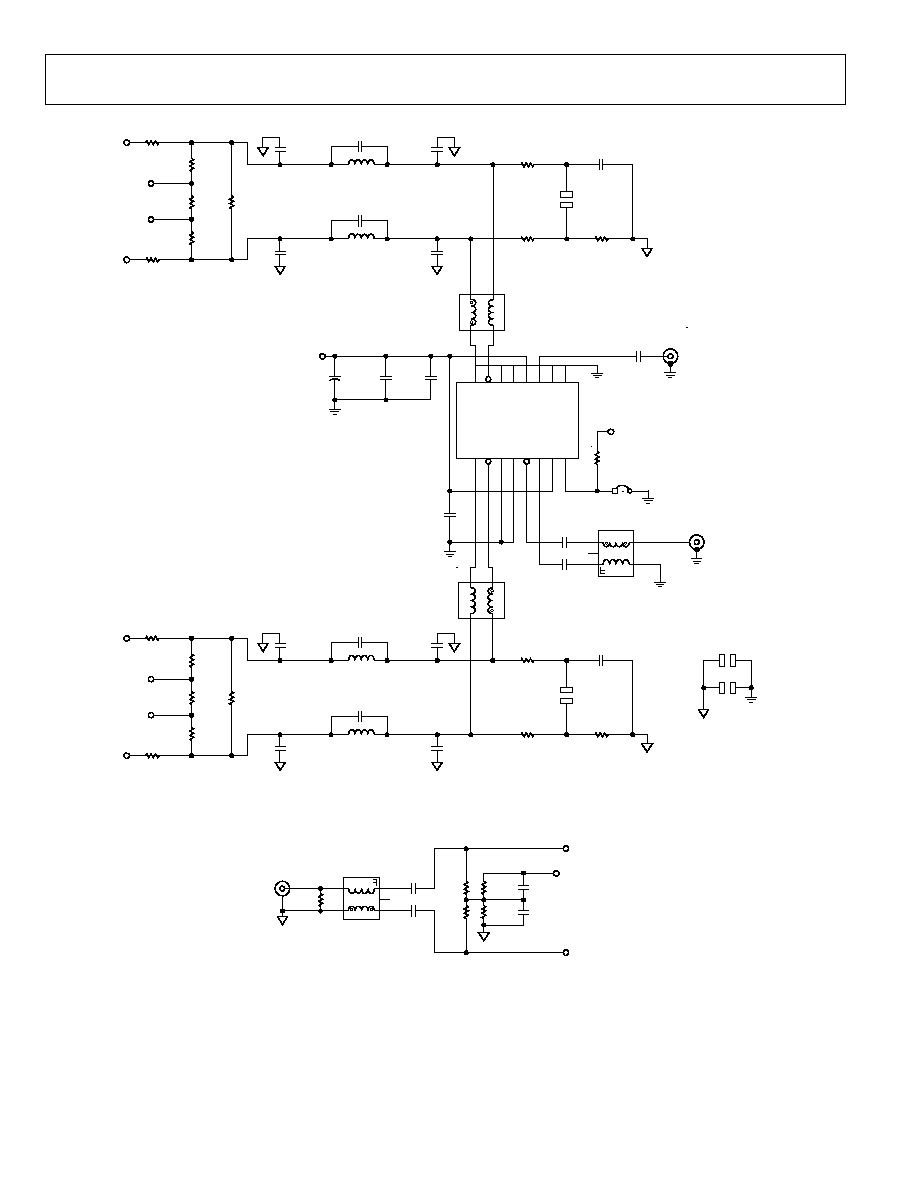
AD9776/AD9778/AD9779
Rev. 0 | Page 50 of 56
G2
E
NBL
VPS1
G1A
G1B
LOIP
VPS2
G4A
G4B
QBBP
VOU
T
G3
IBBP
IBBN
QBBN
LOIN
AD8346
9
8
7
3
4
6
12
13
14
16
11
10
1
21
5
5
U9
VDDM
DGND2
VDDM
R14
1k
JP1
J4
C47
100pF
C72
0.1
F
C72
0.1
F
C41
10
F
10V
2
2
1
DGND2
2
DGND2
2
DGND2
2
DGND2
2
DGND2
DGND2
MODULATED OUTPUT
2
J5
JP9
2
1
DGND2
LOCAL OSC OUTPUT
C74
100pF
C54
0.1
F
C79
17.2pF
C65
17.2pF
C75
100pF
C51
0.1
F
+
JP13
R60
40
R2
150
R3
150
R25
150
R61
40
1
3
P
5
2
S
ETC1-1-13
T4
4
6
4
P
1
S
ADTL1-12
T3
3
JP10
R24
20
R62
147.5
C82
4.5pF
L11
55nH
C43
17.2pF
C44
17.2pF
C83
2.1pF
L10
55nH
R27
300
D2N
D2P
AUX2_P
AUX2_N
R23
20
C53
0.1
F
C52
17.2pF
C50
17.2pF
JP13
R20
40
R4
150
R12
150
R17
150
R21
40
6
4
P
1
S
ADTL1-12
T5
3
R15
20
R22
147.5
C81
4.5pF
L11
55nH
C63
17.2pF
C64
17.2pF
C80
2.1pF
L10
55nH
R19
300
D1N
D1P
AUX1_P
AUX1_N
R16
20
05361-103
Figure 104. Evaluation Board, Rev. D, AD8349 Quadrature Modulator
4
5
S
3
2
R13
VAL
R30
1k
R31
300
R28
25
R29
25
P
ETC1-1-13
T2
C19
0.1
F
C16
DNB
CVDD18
CLK_P
CLK_N
C17
0.1
F
C23
0.1
F
1
05361-104
Figure 105. Evaluation Board, Rev. D, DAC Clock Interface
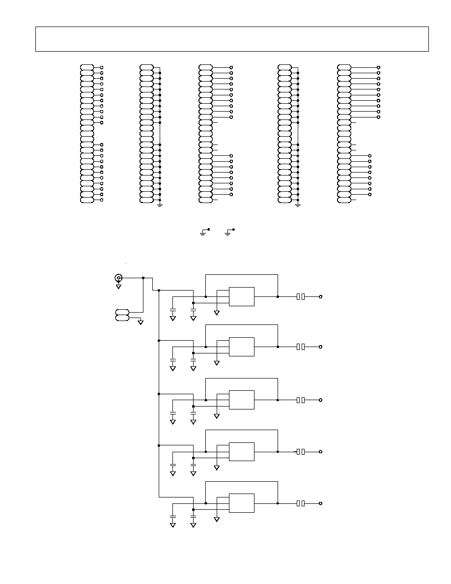
AD9776/AD9778/AD9779
Rev. 0 | Page 51 of 56
A1
P4
PKG_TYPE = MOLEX110
VAL
A2
A3
A4
A5
A6
A7
A8
A9
A10
A11
A15
A16
A17
A18
A19
A20
A21
A22
A23
A24
A25
C1
P4
PKG_TYPE = MOLEX110
VAL
C2
C3
C4
C5
C6
C7
C8
C9
C10
C11
C15
C16
C17
C18
C19
C20
C21
C22
C23
C24
C25
CSB
SD1
P2D0
P2D2
P2D4
P2D6
P2D8
P2D10
P2D12
P2D14
P1D0
P1D2
P1D4
P1D6
P1D8
P1D10
P1D12
P1D14
DGND
BLK
E1
P4
PKG_TYPE = MOLEX110
VAL
E2
E3
E4
E5
E6
E7
E8
E9
E10
E11
E15
E16
E17
E18
E19
E20
E21
E22
E23
E24
E25
SCLK
SD0
P2D1
P2D3
P2D5
P2D7
P2D9
P2D11
P2D13
P2D15
P1D1
P1D3
P1D5
P1D7
P1D9
P1D11
P1D13
P1D15
B1
P4
PKG_TYPE = MOLEX110
VAL
B2
B3
B4
B5
B6
B7
B8
B9
B10
B11
B15
B16
B17
B18
B19
B20
B21
B22
B23
B24
B25
D1
P4
PKG_TYPE = MOLEX110
VAL
D2
D3
D4
D5
D6
D7
D8
D9
D10
D11
D15
D16
D17
D18
D19
D20
D21
D22
D23
D24
D25
DGND1
BLK
05361-105
Figure 106. Evaluation Board, Rev. D, Digital Input Buffers
VAL
CNTERM_2P
1
2
J2
1
2
3
4
U2
A DP3339-1-8
CVDD18_IN
JP19
C85
1
F
C86
1
F
1
P2
2
1
2
3
4
U8
A DP3339-3-3
DPWR33_IN
JP23
C97
1
F
C96
1
F
1
2
3
4
U7
A DP3339-3-3
AVDD33_IN
JP22
C94
1
F
C93
1
F
1
2
3
4
U4
A DP3339-3-3
DVDD33_IN
JP21
C91
1
F
C92
1
F
1
2
3
4
U3
A DP3339-1-8
DVDD18_IN
JP20
C88
1
F
C89
1
F
05361-106
Figure 107. Evaluation Board, On-Board Voltage Regulators

AD9776/AD9778/AD9779
Rev. 0 | Page 52 of 56
05361-107
Figure 108. Evaluation Board, Rev. D, Top Silk Screen
05361-108
Figure 109. Evaluation Board, Rev. D, Top Layer

AD9776/AD9778/AD9779
Rev. 0 | Page 53 of 56
05361-109
Figure 110. Evaluation Board, Rev. D, Layer 2
05361-110
Figure 111. Evaluation Board, Rev. D, Layer 3
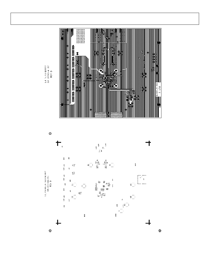
AD9776/AD9778/AD9779
Rev. 0 | Page 54 of 56
05361-111
Figure 112. Evaluation Board, Rev. D, Bottom Layer
05361-112
Figure 113. Evaluation Board, Rev. D, Bottom Silkscreen

AD9776/AD9778/AD9779
Rev. 0 | Page 55 of 56
OUTLINE DIMENSIONS
COMPLIANT TO JEDEC STANDARDS MS-026-AED-HD
0.27
0.22
0.17
1
25
26
49
76
100
75
50
14.00 BSC SQ
16.00 BSC SQ
0.50 BSC
LEAD PITCH
0.75
0.60
0.45
1.20
MAX
1
25
26
50
76
100
75
51
1.05
1.00
0.95
0.20
0.09
0.08 MAX
COPLANARITY
VIEW A
ROTATED 90
°
CCW
SEATING
PLANE
0° MIN
7°
3.5°
0°
0.15
0.05
VIEW A
PIN 1
TOP VIEW
(PINS DOWN)
BOTTOM VIEW
(PINS UP)
9.50 SQ
EXPOSED
PAD
Figure 114. 100-Lead Thin Quad Flat Package, Exposed Pad [TQFP_EP]
(SV-100-3)
Dimensions shown in millimeters
ORDERING GUIDE
Model
Temperature Range
Package Description
Package Option
AD9776BSVZ
1
40
°C to +85°C
100-lead TQFP_EP
SV-100-3
AD9776BSVZRL
1
40
°C to +85°C
100-lead TQFP_EP
SV-100-3
AD9778BSVZ
1
40
°C to +85°C
100-lead TQFP_EP
SV-100-3
AD9778BSVZRL
1
40
°C to +85°C
100-lead TQFP_EP
SV-100-3
AD9779BSVZ
1
40
°C to +85°C
100-lead TQFP_EP
SV-100-3
AD9779BSVZRL
1
40
°C to +85°C
100-lead TQFP_EP
SV-100-3
AD9776-EB
Evaluation
Board
AD9778-EB
Evaluation
Board
AD9779-EB
Evaluation
Board
1
Z = Pb-free part.

AD9776/AD9778/AD9779
Rev. 0 | Page 56 of 56
NOTES
© 2005 Analog Devices, Inc. All rights reserved. Trademarks and
registered trademarks are the property of their respective owners.
D05361-0-7/05(0)