
250MHz General Purpose
Low Cost, DC Coupled VGA
Preliminary Data Sheet
AD8337
Rev. PrA
4/26/2005
Information furnished by Analog Devices is believed to be accurate and reliable.
However, no responsibility is assumed by Analog Devices for its use, nor for any
infringements of patents or other rights of third parties that may result from its use.
Specifications subject to change without notice. No license is granted by implication
or otherwise under any patent or patent rights of Analog Devices. Trademarks and
registered trademarks are the property of their respective owners.
One Technology Way, P.O. Box 9106, Norwood, MA 02062-9106, U.S.A.
Tel: 781.329.4700
www.analog.com
Fax: 781.326.8703
ę 2005 Analog Devices, Inc. All rights reserved.
OUTP
GAIN
INPP
GAIN CONTROL
INTERFACE
INPN
PRAO
3
4
2
5
7
1
VCOM
8
6
VNEG
VPOS
FEATURES
Low Noise
Voltage noise = 2.2 nV/Hz
Current noise = 2.5 pA/Hz (Positive Input)
Wide Bandwidth (-3 dB) = 250 MHz
Nominal Gain Range
0 dB to 24 dB (Preamp Gain = 6 dB)
Gain Scaling
20 dB/V
DC Coupled
Single Ended Input and Output
Supplies: +5V, +/-2.5V or +/-5V
Low power: 78 mW
APPLICATIONS
Gain Trim
PET Scanners
High performance AGC systems
I/Q signal processing
Video
Industrial and Medical Ultrasound
Radar Receivers
GENERAL DESCRIPTION
The AD8337 is a low noise single ended linear-in-dB, general
purpose variable gain amplifier usable as a low noise variable
gain element at frequencies up to 100 MHz; the ş3 dB
bandwidth is 250 MHz.
The topology used is an X-AMP« structure with 24 dB of gain
range. The VGA is intended for trim applications. Excellent
bandwidth uniformity is maintained across the entire range.
The gain control interface provides precise linear-in-dB scaling
of 20 dB/V and is centered on VCOM. The VGA's low output-
referred noise is advantageous in driving high speed ADCs.
Excellent DC characteristics and high speed make the AD8337
particularly suited for industrial ultrasound, PET scanners, and
for video applications. Dual supply operation enables gain
control of negative-going pulses such as generated by
photodiodes or photo-multiplier tubes.
FUNCTIONAL BLOCK DIAGRAM
Figure 1. AD8337 Functional Block Diagram and Pinout
The AD8337 contains an operational amplifier (preamplifier ş
PrA) at its input which can be configured for any gain greater
than two with external resistors, this allows both inverting and
non-inverting topologies and thereby a dual polarity VGA. The
VGA is specified with a non-inverting PrA gain-of-2. The
attenuator has a range of 24 dB and the output amplifier has a
gain-of-8 (18.06 dB). Because the preamplifier gain can be set
through external resistors, the gain range will shift up or down
depending on the PrA gain, nominally the gain range is from 0
to +24 dB.
For larger gain ranges, multiple VGAs can be connected in
series. This also allows for interstage filtering to suppress noise
and distortion.
The operating temperature range is ş40░C to +85░. The
AD8337 is available in a 3x3 mm 8 pin chip-scale package
(CSP).

AD8337
Preliminary Data Sheet
Rev. PrA | Page 2 of 9
TABLE OF CONTENTS
AD8337--Specifications.................................................................. 3
Absolute Maximum Ratings............................................................ 5
Pin Configuration and Functional Descriptions.......................... 6
ESD CAUTION ............................................................................ 6
Theory Of Operation ....................................................................... 7
Preamplifier................................................................................... 7
VGA................................................................................................ 7
Gain Control ................................................................................. 7
Attenuator.......................................................................................7
Output Stage...................................................................................7
Single Supply Operation/ AC coupling ......................................8
Noise ...............................................................................................8
Applications........................................................................................9
Driving Capacitive Loads.............................................................9
Board Layout..................................................................................9
REVISION HISTORY
Rev. PrA:

Preliminary Data Sheet
AD8337
Rev. PrA | Page 3 of 9
AD8337--SPECIFICATIONS
Table 1. V
S
= ▒2.5 V, T
A
= 25░C, PrA Gain = +2 (R
FB1
= R
FB2
= 100 ), V
COM
= GND; f = 10 MHz, C
L
= 10 pF, R
L
= 500 , unless
otherwise specified.
Parameter Conditions
Min
Typ
1
Max
Unit
GENERAL PARAMETERS
ş3 dB Small Signal Bandwidth
V
OUT
= 10 mV p-p
250
MHz
ş3 dB Large Signal Bandwidth
V
OUT
= 1 V p-p
190
MHz
Slew Rate
V
OUT
= 2 V p-p square wave
475
V/Ás
V
OUT
= 1 V p-p square wave
375
V/Ás
Input Voltage Noise
f = 10 MHz
2.2
nV/Hz
Input Current Noise
f = 10 MHz
2.5
pA/Hz
Noise Figure
V
GAIN
= 0.7 V, R
S
= 50 , unterminated
8
dB
V
GAIN
= 0.7 V, R
S
= 1k, unterminated
2
dB
Output-Referred Noise
V
GAIN
= 0.7 V (Gain = 24 dB)
34
nV/Hz
V
GAIN
= -0.7 V (Gain = 0 dB)
17.5
nV/Hz
Output Impedance
DC to 10 MHz
0.7+j1.3
Output Signal Range
R
L
500 , Vsupply =
▒ 2.5 V, + 5V
V
COM
▒ 1.4
V
R
L
500 , Vsupply =
▒ 5 V
V
COM
▒ 3.4
V
Output Offset Voltage
V
GAIN
= 0.7 V (Gain = 24 dB)
TBD
<20
TBD
mV
DYNAMIC PERFORMANCE
V
S
= ▒2.5V
Harmonic Distortion
V
GAIN
= 0V, V
OUT
= 1 Vpp
HD2
f = 1 MHz
-64
dBc
HD3
-66
dBc
HD2
f = 10 MHz
-63
dBc
HD3
-61
dBc
HD2
f = 45 MHz
-61
dBc
HD3
-72
dBc
Output 1 dB Compression Point
V
GAIN
= -0.7 V, f = 10 MHz
+9.5
dBm
2
V
GAIN
= +0.7 V, f = 10 MHz
+15.8
dBm
V
GAIN
= 0 V, V
OUT
= 1 Vpp, f
1
= 10 MHz, f
2
= 11 MHz
-72
dBc
Two-Tone Intermodulation
Distortion (IMD3)
V
GAIN
= 0, V
OUT
= 1 Vpp, f
1
= 45 MHz, f
2
= 46 MHz
-58
dBc
V
GAIN
= 0, V
OUT
= 2 Vpp, f
1
= 10 MHz, f
2
= 11 MHz
-61
dBc
V
GAIN
= 0, V
OUT
= 2 Vpp, f
1
= 45 MHz, f
2
= 46 MHz
-45
dBc
V
GAIN
= 0, V
OUT
= 1 Vpp, f = 10 MHz
33
dBm
Output Third Order Intercept
V
GAIN
= 0, V
OUT
= 1 Vpp, f = 45 MHz
26
dBm
V
GAIN
= 0, V
OUT
= 2 Vpp, f = 10 MHz
34
dBm
V
GAIN
= 0, V
OUT
= 2 Vpp, f = 45 MHz
26
dBm
Overload Recovery
V
GAIN
= 0.7 V, V
IN
= 50 - 500 mV p-p
50
ns
Group Delay Variation
1 MHz < f < 100 MHz, Full Gain Range
▒TBD
ns
DYNAMIC PERFORMANCE
V
S
= ▒5V
Harmonic Distortion
V
GAIN
= 0V, V
OUT
= 1 Vpp
HD2
f = 1 MHz
-68
dBc
HD3
-68
dBc
HD2
f = 10 MHz
-73
dBc
HD3
-65
dBc
HD2
f = 45 MHz
-63
dBc
HD3
-69
dBc
Output 1 dB Compression Point
V
GAIN
= -0.7 V, f = 10 MHz
15.8
dBm
V
GAIN
= +0.7 V, f = 10 MHz
23.4
dBm
Two-Tone Intermodulation
V
GAIN
= 0 V, V
OUT
= 1 Vpp, f
1
= 10 MHz, f
2
= 11 MHz
-75
dBc
1
Bold/Italic
values are measured, all others are simulated and still need to be confirmed.
2
All dBm values are calculated with 50 reference, unless otherwise noted.

AD8337
Preliminary Technical Data
Rev. PrA | Page 4 of 9
Parameter Conditions
Min
Typ
1
Max
Unit
Distortion (IMD3)
V
GAIN
= 0, V
OUT
= 1 Vpp, f
1
= 45 MHz, f
2
= 46 MHz
-60
dBc
V
GAIN
= 0, V
OUT
= 2 Vpp, f
1
= 10 MHz, f
2
= 11 MHz
-64
dBc
V
GAIN
= 0, V
OUT
= 2 Vpp, f
1
= 45 MHz, f
2
= 46 MHz
-48
dBc
V
GAIN
= 0, V
OUT
= 1 Vpp, f = 10 MHz
34
dBm
Output Third Order Intercept
V
GAIN
= 0, V
OUT
= 1 Vpp, f = 45 MHz
27
dBm
V
GAIN
= 0, V
OUT
= 2 Vpp, f = 10 MHz
35
dBm
V
GAIN
= 0, V
OUT
= 2 Vpp, f = 45 MHz
27
dBm
Overload Recovery
V
GAIN
= 0.7 V, V
IN
= 0.1 - 1 V p-p
TBD
ns
Group Delay Variation
1 MHz < f < 100 MHz, Full Gain Range
▒TBD
ns
ACCURACY
-0.7 V < V
GAIN
< -0.6 V
TBD
TBD
TBD
dB
-0.6 V < V
GAIN
< 0.6 V
TBD
▒0.25
TBD
dB
Absolute Gain Error
3
0.6 V < V
GAIN
< 0.7 V
TBD
TBD
TBD
dB
Gain Law Conformance
4
-0.5 V < V
GAIN
< 0.5 V
TBD
dB
GAIN CONTROL INTERFACE
Gain Range
24
dB
Gain Scaling Factor
20
dB/V
Gain Intercept
V
GAIN
= 0 V
12.5
dB
Input Voltage (V
GAIN
) Range
No foldover
-V
S
V
S
V
Input Impedance
TBD
M
Response Time
24 dB Gain Change
TBD
ns
POWER SUPPLY
Supply Voltage
V
POS
- V
NEG
(dual and single supply operation)
|4.5|
|5|
|10|
V
Quiescent Current
Each Supply (VPOS and VNEG)
15.5
mA
Power Dissipation
No Signal, VPOS-VNEG = 5V
78
mW
PSRR V
GAIN
= 0.7 V, f = 10 MHz
-35
dB
Vsupply = ▒5V
Quiescent Current
Each Supply (VPOS and VNEG)
18.5
mA
Power Dissipation
No Signal, V
S
= ▒5V
185
mW
PSRR V
GAIN
= 0.7 V, f = 10 MHz
TBD
dB
3
Conformance to theoretical gain expression (see Equation 1).
4
Conformance to best fit dB linear curve.

Preliminary Data Sheet
AD8337
Rev. PrA | Page 5 of 9
ABSOLUTE MAXIMUM RATINGS
Table 2. Absolute Maximum Ratings
Parameter Rating
Voltage
Supply Voltage (VPOS, VNEG)
▒6V
Input Voltage (INPx)
TBD V
GAIN Voltage
VPOS, VNEG
Power Dissipation
TBD W
Temperature
Operating Temperature
ş40░C to +85░C
Storage Temperature
ş65░C to +150░C
Lead Temperature (Soldering 60 sec)
300░C
JA
xx Package
5
TBD░C/W
5
Four-Layer JEDEC Board (2S2P).
Stresses above those listed under the Absolute Maximum
Ratings may cause permanent damage to the device. This is a
stress rating only; functional operation of the device at these or
any other conditions above those indicated in the operational
section of this specification is not implied. Exposure to absolute
maximum rating conditions for extended periods may affect
device reliability.
AD8337
Preliminary Technical Data
Rev. PrA | Page 6 of 9
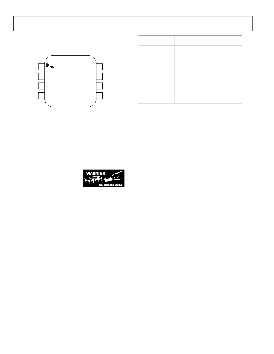
PIN CONFIGURATION AND FUNCTIONAL
DESCRIPTIONS
1
2
3
4
8
7
6
5
VOUT
VCOM
INPP
INPN
VPOS
GAIN
VNEG
PRAO
Pin 1
Identifier
AD8337
Top View
(not to scale)
Figure 1.
8 LFCSP
Table 3. Pin Function Descriptions
Pin
No.
Mnemonic Function
1
VOUT
VGA Output
2
VCOM
Common ş Ground for Dual Supply;
Apply VPOS/2 for Single Supply
3
INPP
Positive Input to Preamplifier
4
INPN
Negative Input to Preamplifier
5
PRAO
Preamplifier Output
6
VNEG
Negative Supply (-VPOS for Dual
Supply; GND for Single Supply)
7
GAIN
Gain Control Input centered at
VCOM
8
VPOS
Positive Supply
ESD CAUTION
ESD (electrostatic discharge)
sensitive device. Electrostatic
charges as high as 4000 V readily
accumulate on the human body and
test equipment and can discharge
without detection. Although this
product features proprietary ESD
protection circuitry, permanent
damage may occur on devices
subjected to high energy
electrostatic discharges. Therefore,
proper ESD precautions are
recommended to avoid performance
degradation or loss of functionality.

Preliminary Data Sheet
AD8337
Rev. PrA | Page 7 of 9
THEORY OF OPERATION
The AD8337 is a low noise single ended linear-in-dB, general
purpose variable gain amplifier (VGA) usable as a low noise
variable gain element at frequencies up to 100 MHz; the ş3 dB
bandwidth is 250 MHz. It is fabricated in an ADI proprietary
dielectrically isolated complementary bipolar process with f
T
s
in the 3- 5 GHz range. The part is DC coupled throughout and
has relatively low offset even at maximum gain. The power
consumption is very low at only 78 mW on a 5 V supply (either
single +5 V or
▒2.5 V); the supply current is typically
about15.5 mA in this case.
Figure 2 shows the circuit block diagram of the AD8337.
VOUT
INPP
INPL
VPOS
VNEG
Interpolator
GAIN Interface
PrA
-
+
BIAS
Attenuator
-24 to 0 dB
+
-
-
+
GAIN
PRAO
VCOM
Outamp
18dB (x8)
Rs
Rfb1
Rfb2
Preamp
6dB (nominally)
R1 = 107
R2 = 749
Figure 2.
Block Diagram of the AD8337
PREAMPLIFIER
The AD8337 also includes a current feedback preamplifier that
buffers the ladder network of the X-AMP
«
. External resistor
can be used to set the gain of the preamplifier but it is specified
with a non-inverting gain-of-2 with Rfb1 = Rfb2 = 100
. Other gains can be implemented, however, it is important to
not use a smaller value for Rfb2 than 100
because Rfb2
along with an internal compensation capacitor determines the -
3 dB bandwidth of the preamplifier. If a smaller resistor is used,
the preamplifier may go unstable. Larger values for Rfb2 will
reduce the bandwidth and increase the preamplifier gain; this
allows the user to shift the 24 dB gain range up from the
nominal 0 ş 24 dB range. Increasing the preamplifier gain will
increase the offset because of the DC coupling. The only other
thing to watch out for is that if Rfb1 also is increased then the
input referred noise will increase, otherwise the preamplifier
can be thought of as an uncommitted op-amp that is greater
than gain-of-2 stable.
VGA
The VGA is a standard X-AMP architecture which has a linear-
in-dB gain characteristic. This architecture has been proven to
give the best output dynamic range in receive applications. As
can be seen in Figure 2, the variable attenuator range is 24 dB,
this is then followed by a fixed gain amplifier of 18 dB for a
total VGA gain range of -6 dB to +18 dB. Together with the
preamplifier configured with a gain of 6 dB, this results in the
specified gain range of 0 to +24 dB.
The VGA plus preamp with 6 dB of gain implements a gain
law as follows:
)
(
20
)
(
dB
ICPT
Vgain
V
dB
dB
Gain
+
=
,
where the nominal intercept (ICPT) is 12.15 dB. If the gain of
the preamp is increased then ICPT will increase accordingly.
For example, if the gain of the preamp is increased by 6 dB,
then ICPT will shift up by 6 dB to 18.15 dB.
GAIN CONTROL
The gain control interface provides a high impedance input and
is referenced to pin VCOM which for maximum output swing
should be always mid-supply at (VPOS+VNEG)/2. In a dual
supply configuration, as in the low power configuration with
▒2.5 V supplies, this would be ground. The voltage on pin
VCOM determines the midpoint of the gain range which
normally runs from -0.7 to +0.7 V with the most linear-in-dB
section of the gain control running from about -0.6 to +0.6 V.
In this middle section the gain error is typically less than
▒0.2
dB. The gain control voltage can be increased or decreased to
the positive and negative supply voltages without gain foldover.
The gain scaling factor (gain slope) is 20 dB/V, this relatively
low slope ensures that noise on the GAIN input will not be
unduly amplified. Since a VGA is really a multiplier it is
important to make sure that the GAIN input does not
accidentally modulate the output signal because of some
unwanted signal coupling onto the gain control line. Because of
the high input impedance of the GAIN input it is easy to add a
simple low pass filter to eliminate any unwanted signal on the
gain control input.
ATTENUATOR
The attenuator in the VGA presents an input resistance of
nominally 265
s to the preamplifier, this together with the
external 200
s of Rfb1 and Rfb2 results in an effective load of
about 114
that the preamplifier has to drive. The attenuator is
made up of eight -3.01 dB sections for a total attenuation range
of -24.08 dB. Following the attenuator is a fixed gain amplifier
with x8 gain. Because of this relatively low gain, the output
offset is kept well below 20 mV even over temperature; the
offset is largest at max gain since then the preamplifier offset is
amplified. The VCOM pin defines the common-mode reference
for the output as seen in Figure 2.
OUTPUT STAGE
The output stage of the VGA is similar to the preamplifier and
is very high speed. It is a Class AB complementary emitter
follower type output stage; these stages tend to look inductive
(increasing impedance) with increasing frequency because of
the AC-beta roll-off of the output devices and the inherent
reduction in feedback beyond the -3 dB point. High speed
output stages like this tend to be able to drive large currents,
however, they are also more susceptible to capacitive loading.
A small series resistor can reduce the effects of capacitive
loading (see Application section).

AD8337
Preliminary Technical Data
Rev. PrA | Page 8 of 9
SINGLE SUPPLY OPERATION/ AC COUPLING
If a user wants to run the AD8337 from a single +5 V supply,
then VCOM needs to be biased from a good 2.5 V reference,
especially if the part is still DC coupled; the voltage source
applied to VCOM needs to be able to handle the currents that
flow in the load of the preamplifier and the output stage of the
VGA. In the event that a user wants to AC couple the AD8337,
it is essential that some bias network is provided to pin INPP.
In that case the bias generator for pin VCOM "only" needs to
be able to supply the dynamic current to the preamplifier
feedback network and the gain setting resistors of the VGA. For
most single +5 V supply applications, if no +2.5 V supply is
available, it will be necessary to use a good op-amp with
enough current drive capability and possibly a reference like
the ADR431.
NOISE
The total input referred noise is about 2.2 nV/
Hz and the
current noise about 2.5 pA/
Hz on the positive preamp input,
INPP. The VGA output referred noise is about 15 nV/
Hz at
low gains, this result divided by the VGA fixed gain amplifier
gain of x8, results in about 1.9 nV/
Hz referred to the VGA
input. Note that this value includes the noise of the VGA gain
setting resistors as well. If this voltage is again divided by the
preamp gain-of-2, then the VGA noise referred all the way to
the preamp input is about 0.8 nV/
Hz. From this we can
determine that the preamplifier, including the 100
gain
setting resistors, contribute about 2 nV/
Hz. The two 100
resistors contribute each 1.29 nV/
Hz at the output of the
preamp, when this is divided down by 2 and subtracted, then
the preamplifier noise can be determined at about 1.75 nV/
Hz.
The following equation shows the calculation that determines
the output referred noise at max gain (24 dB or x16): A
t
= total
gain from preamp input to VGA output; R
S
= source resistance;
e
n-PrA
= input referred voltage noise of preamp; i
n-PrA
= current
noise of preamp at INPP pin; e
n-Rfb1
= voltage noise of Rfb1; e
n-
Rfb2
= voltage noise of Rfb2; e
n-VGA
= input referred voltage
noise of VGA (low gain output referred noise divided by fixed
gain of x8).
(
)
2
2
2
2
1
2
Pr
2
Pr
2
)
(
)
(
)
1
2
(
)
(
)
(
VGA
VGA
n
VGA
Rfb
n
VGA
Rfb
n
S
A
n
t
A
n
t
S
out
n
A
e
A
e
A
Rfb
Rfb
e
R
i
A
e
A
R
e
+
+
+
+
+
=
-
-
-
-
-
-
This simplifies to the following if R
S
= 0, Rfb1 = Rfb2 = 100
, A
t
= 16, A
VGA
= 8.
Hz
nV
e
out
n
/
35
)
8
9
.
1
(
)
8
29
.
1
(
2
)
16
75
.
1
(
2
2
2
=
+
+
=
-
.
Taking this result and dividing by 16 gives the total input
referred noise with a short circuited input as 2.2 nV/
Hz. When
the preamplifier is used in the inverting configuration with the
same Rfb1 and Rfb2 = 100
as above then e
n-out
does not
change, however, because the gain dropped by 6 dB, the input
referred noise increases by a factor-of-2 to about 4.4 nV/
Hz.
The reason for this is that the noise gain to the output of all the
noise generators stays the same, yet the preamp in the inverting
configuration has a gain of (-1) compared to the (+2) in the
non-inverting configuration; this increases the input referred
noise by two.

Preliminary Data Sheet
AD8337
Rev. PrA | Page 9 of 9
APPLICATIONS
DRIVING CAPACITIVE LOADS
Because of the large bandwidth of the AD8337, when driving
capacitive loads, there may be excessive peaking beyond 100
MHz. This peaking can be mitigated by using a series resistor at
the output, R
SNUB
, to isolate the cap load. The only disadvantage
of this method is the attenuation introduced by the attenuator
that is formed between R
SNUB
and R
LOAD
, where the attenuation
factor is R
LOAD
/( R
SNUB
+ R
LOAD
).
The preamplifier also is sensitive to cap loads; however, this is
typically not an issue since only the gain setting resistors load it.
If it is desired to drive a capacitive load directly from the
preamplifier, then it is recommended that the user also inserts a
small series resistor between this cap load and the preamp
output.
BOARD LAYOUT
Because the AD8337 is a high frequency device board layout is
critical. In particular it is important to have good ground plane
connection to the VCOM pin. Also the ground for the VGA
output and should be separated from the ground for the preamp
gain setting resistors and the VCOM pin. Coupling through the
ground plane from the output to the input can cause peaking at
higher frequencies. For layout reasons it helps to visualize how
and where the load currents are flowing, this way one can see
potential interaction between output and input.
PR05575-0-5/05(PrA)