Äîêóìåíòàöèÿ è îïèñàíèÿ www.docs.chipfind.ru
Low Noise Rail-to-Rail
Differential ADC Driver
AD8139
Rev. A
Information furnished by Analog Devices is believed to be accurate and reliable.
However, no responsibility is assumed by Analog Devices for its use, nor for any
infringements of patents or other rights of third parties that may result from its use.
Specifications subject to change without notice. No license is granted by implication
or otherwise under any patent or patent rights of Analog Devices. Trademarks and
registered trademarks are the property of their respective owners.
One Technology Way, P.O. Box 9106, Norwood, MA 02062-9106, U.S.A.
Tel: 781.329.4700
www.analog.com
Fax: 781.326.8703
© 2004 Analog Devices, Inc. All rights reserved.
FEATURES
Fully differential
Low noise
2.25 nV/Hz
2.1 pA/Hz
Low harmonic distortion
98 dBc SFDR @ 1 MHz
85 dBc SFDR @ 5 MHz
72 dBc SFDR @ 20 MHz
High speed
410 MHz, 3 dB BW (G = 1)
800 V/µs slew rate
45 ns settling time to 0.01%
69 dB output balance @ 1 MHz
80 dB dc CMRR
Low offset: ±0.5 mV max
Low input offset current: 0.5 µA max
Differential input and output
Differential-to-differential or single-ended-to-differential
operation
Rail-to-rail output
Adjustable output common-mode voltage
Wide supply voltage range: 5 V to 12 V
Available in small SOIC package
APPLICATIONS
ADC drivers to 18 bits
Single-ended-to-differential converters
Differential filters
Level shifters
Differential PCB board drivers
Differential cable drivers
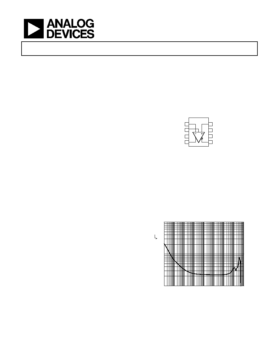
FUNCTIONAL BLOCK DIAGRAM
04679-0-001
IN
1
V
OCM
2
V+
3
+OUT
4
+IN
8
NC
7
V
6
OUT
5
NC = NO CONNECT
AD8139
Figure 1.
GENERAL DESCRIPTION
The AD8139 is an ultralow noise, high performance differential
amplifier with rail-to-rail output. With its low noise, high SFDR,
and wide bandwidth, it is an ideal choice for driving ADCs with
resolutions to 18 bits. The AD8139 is easy to apply, and its in-
ternal common-mode feedback architecture allows its output
common-mode voltage to be controlled by the voltage applied
to one pin. The internal feedback loop also provides out-
standing output balance as well as suppression of even-order
harmonic distortion products. Fully differential and single-
ended-to-differential gain configurations are easily realized by
the AD8139. Simple external feedback networks consisting of a
total of four resistors determine the amplifier's closed-loop gain.
The AD8139 is manufactured on ADI's proprietary second gen-
eration XFCB process, enabling it to achieve low levels of distor-
tion with input voltage noise of only 1.85 nV/Hz.
The AD8139 is available in an 8-lead SOIC package with an
exposed paddle (EP) on the underside of its body and a 3 mm ×
3 mm LFCSP. It is rated to operate over the temperature range
of -40°C to +125°C.
1
10
100
1k
10k
100k
1M
10M
1G
100M
10
100
04679-0-078
FREQUENCY (Hz)
IN
PU
T VOLTA
G
E N
O
ISE (
n
V/ H
z
)
Figure 2. Input Voltage Noise vs. Frequency

AD8139
Rev. A | Page 2 of 24
TABLE OF CONTENTS
V
S
= ±5 V, V
OCM
= 0 V Specifications.............................................. 3
V
S
= 5 V, V
OCM
= 2.5 V Specifications ............................................. 5
Absolute Maximum Ratings............................................................ 7
Thermal Resistance ...................................................................... 7
ESD Caution.................................................................................. 7
Pin Configuration and Function Descriptions............................. 8
Typical Performance Characteristics ............................................. 9
Theory of Operation ...................................................................... 18
Typical Connection and Definition of Terms ........................ 18
Applications..................................................................................... 19
Estimating Noise, Gain, and Bandwidth with Matched
Feedback Networks .................................................................... 19
Outline Dimensions ....................................................................... 24
Ordering Guide .......................................................................... 24
REVISION HISTORY
8/04--Data Sheet Changed from a Rev. 0 to Rev. A.
Added 8-Lead LFCSP.........................................................Universal
Changes to General Description .................................................... 1
Changes to Figure 2.......................................................................... 1
Changes to V
S
= ±5 V, V
OCM
= 0 V Specifications ......................... 3
Changes to V
S
= 5 V, V
OCM
= 2.5 V Specifications......................... 5
Changes to Table 4............................................................................ 7
Changes to Maximum Power Dissipation Section....................... 7
Changes to Figure 26 and Figure 29............................................. 12
Inserted Figure 39 and Figure 42.................................................. 14
Changes to Figure 45 to Figure 47................................................ 15
Inserted Figure 48........................................................................... 15
Changes to Figure 52 and Figure 53............................................. 16
Changes to Figure 55 and Figure 56............................................. 17
Changes to Table 6.......................................................................... 19
Changes to Voltage Gain Section.................................................. 19
Changes to Driving a Capacitive Load Section .......................... 22
Changes to Ordering Guide .......................................................... 24
Updated Outline Dimensions ....................................................... 24
5/04--Revision 0: Initial Version

AD8139
Rev. A | Page 3 of 24
V
S
= ±5 V, V
OCM
= 0 V SPECIFICATIONS
@ 25°C, Diff. Gain = 1, R
L, dm
= 1 k, R
F
= R
G
= 200 , unless otherwise noted. T
MIN
to T
MAX
= -40°C to +125°C.
Table 1.
Parameter Conditions
Min
Typ
Max
Unit
DIFFERENTIAL INPUT PERFORMANCE
DYNAMIC PERFORMANCE
-3 dB Small Signal Bandwidth
V
O, dm
= 0.1 V p-p
340
410
MHz
-3 dB Large Signal Bandwidth
V
O, dm
= 2 V p-p
210
240
MHz
Bandwidth for 0.1 dB Flatness
V
O, dm
= 0.1 V p-p
45
MHz
Slew Rate
V
O, dm
= 2 V Step
800
V/µs
Settling Time to 0.01%
V
O, dm
= 2 V Step, C
F
= 2 pF
45
ns
Overdrive Recovery Time
G = 2, V
IN, dm
= 12 V p-p Triangle Wave
30
ns
NOISE/HARMONIC PERFORMANCE
SFDR V
O, dm
= 2 V p-p, f
C
= 1 MHz
98
dB
V
O, dm
= 2V p-p, f
C
= 5 MHz
85
dB
V
O, dm
= 2 V p-p, f
C
= 20 MHz
72
dB
Third-Order IMD
V
O, dm
= 2 V p-p, f
C
= 10.05 MHz ± 0.05 MHz
-90
dBc
Input Voltage Noise
f = 100 KHz
2.25
nV/Hz
Input Current Noise
f = 100 KHz
2.1
pA/Hz
DC PERFORMANCE
Input Offset Voltage
V
IP
= V
IN
= V
OCM
= 0 V
-500 ±150
+500 µV
Input Offset Voltage Drift
T
MIN
to T
MAX
1.25
µV/ºC
Input Bias Current
T
MIN
to T
MAX
2.25
8.0
µA
Input Offset Current
0.12
0.5
µA
Open-Loop Gain
114
dB
INPUT CHARACTERISTICS
Input Common-Mode Voltage Range
-4
+4
V
Input Resistance
Differential
600
k
Common
Mode
1.5
M
Input Capacitance
Common Mode
1.2
pF
CMRR V
ICM
= ±1 V dc, R
F
= R
G
= 10 k
80
84
dB
OUTPUT CHARACTERISTICS
Output Voltage Swing
Each Single-Ended Output, R
F
= R
G
= 10 k
-V
S
+ 0.20
+V
S
0.20
V
Each Single-Ended Output,
R
L, dm
= Open Circuit, R
F
= R
G
= 10 k
-V
S
+ 0.15
+V
S
0.15
V
Output Current
Each Single-Ended Output
100
mA
Output Balance Error
f = 1 MHz
-69
dB
V
OCM
to V
O, cm
PERFORMANCE
V
OCM
DYNAMIC PERFORMANCE
-3 dB Bandwidth
V
O, cm
= 0.1 V p-p
515
MHz
Slew Rate
V
O, cm
= 2 V p-p
250
V/µs
Gain
0.999
1.000
1.001
V/V
V
OCM
INPUT CHARACTERISTICS
Input Voltage Range
-3.8
+3.8
V
Input Resistance
3.5
M
Input Offset Voltage
V
OS, cm
= V
O, cm
- V
OCM
; V
IP
= V
IN
= V
OCM
= 0 V
-900
±300
+900
µV
Input Voltage Noise
f = 100 kHz
3.5
nV/Hz
Input Bias Current
1.3
4.5
µA
CMRR V
OCM
/V
O, dm
, V
OCM
= ±1 V
74
88
dB

AD8139
Rev. A | Page 4 of 24
Parameter Conditions
Min
Typ
Max
Unit
POWER SUPPLY
Operating Range
4.5
±6
V
Quiescent Current
24.5
25.5
mA
+PSRR
Change in +V
S
= ±1V
95
112
dB
-PSRR
Change in -V
S
= ±1V
95
109
dB
OPERATING TEMPERATURE RANGE
-40
+125
°C

AD8139
Rev. A | Page 5 of 24
V
S
= 5 V, V
OCM
= 2.5 V SPECIFICATIONS
@ 25°C, Diff. Gain = 1, R
L, dm
= 1 k, R
F
= R
G
= 200 , unless otherwise noted. T
MIN
to T
MAX
= -40°C to +125°C.
Table 2.
Parameter Conditions
Min
Typ
Max
Unit
DIFFERENTIAL INPUT PERFORMANCE
DYNAMIC PERFORMANCE
-3 dB Small Signal Bandwidth
V
O, dm
= 0.1 V p-p
330
385
MHz
-3 dB Large Signal Bandwidth
V
O, dm
= 2 V p-p
135
165
MHz
Bandwidth for 0.1 dB Flatness
V
O, dm
= 0.1 V p-p
34
MHz
Slew Rate
V
O, dm
= 2 V Step
540
V/s
Settling Time to 0.01%
V
O, dm
= 2 V Step
55
ns
Overdrive Recovery Time
G = 2, V
IN, dm
= 7 V p-p Triangle Wave
35
ns
NOISE/HARMONIC PERFORMANCE
SFDR V
O, dm
= 2 V p-p, f
C
= 1 MHz
99
dB
V
O, dm
= 2 V p-p, f
C
= 5 MHz, (R
L
= 800 )
87
dB
V
O, dm
= 2 V p-p, f
C
= 20 MHz, (R
L
= 800 )
75
dB
Third-Order IMD
V
O, dm
= 2 V p-p, f
C
= 10.05 MHz ± 0.05 MHz
-87
dBc
Input Voltage Noise
f = 100 kHz
2.25
nV/Hz
Input Current Noise
f = 100 kHz
2.1
pA/Hz
DC PERFORMANCE
Input Offset Voltage
V
IP
= V
IN
= V
OCM
=0 V
-500 ±150
+500 µV
Input Offset Voltage Drift
T
MIN
to T
MAX
1.25
µV/ºC
Input Bias Current
T
MIN
to T
MAX
2.2
7.5
A
Input Offset Current
0.13
0.5
µA
Open-Loop Gain
112
dB
INPUT CHARACTERISTICS
Input Common-Mode Voltage Range
1
4
V
Input Resistance
Differential
600
K
Common-Mode
1.5
M
Input Capacitance
Common-Mode
1.2
pF
CMRR V
ICM
= ±1 V dc, R
F
= R
G
= 10 k
75
79
dB
OUTPUT CHARACTERISTICS
Output Voltage Swing
Each Single-Ended Output, R
F
= R
G
= 10 k
-V
S
+ 0.15
+V
S
- 0.15
V
Each Single-Ended Output,
R
L, dm
= Open Circuit, R
F
= R
G
= 10 k
-V
S
+ 0.10
+V
S
- 0.10
V
Output Current
Each Single-Ended Output
80
mA
Output Balance Error
f = 1 MHz
-70
dB
V
OCM
to V
O, cm
PERFORMANCE
V
OCM
DYNAMIC PERFORMANCE
-3 dB Bandwidth
V
O, cm
= 0.1 V p-p
440
MHz
Slew Rate
V
O, cm
= 2 V p-p
150
V/s
Gain
0.999
1.000
1.001
V/V
V
OCM
INPUT CHARACTERISTICS
Input Voltage Range
1.0
3.8
V
Input Resistance
3.5
M
Input Offset Voltage
V
OS, cm
= V
O, cm
- V
OCM
; V
IP
= V
IN
= V
OCM
= 2.5 V
-1.0
±0.45
+1.0
mV
Input Voltage Noise
f = 100 KHz
3.5
nV/Hz
Input Bias Current
1.3
4.2
A
CMRR V
OCM
/V
O
(dm), V
OCM
= ±1 V
67
79
dB
Document Outline
- FEATURES
- APPLICATIONS
- FUNCTIONAL BLOCK DIAGRAM
- GENERAL DESCRIPTION
- TABLE OF CONTENTS
- þÿ
- þÿ
- þÿ
- þÿ
- þÿ
- þÿ
- þÿ
- þÿ