/home/web/htmldatasheet/RUSSIAN/html/ad/164342
REV. 0
Information furnished by Analog Devices is believed to be accurate and
reliable. However, no responsibility is assumed by Analog Devices for its
use, nor for any infringements of patents or other rights of third parties that
may result from its use. No license is granted by implication or otherwise
under any patent or patent rights of Analog Devices.
a
AD8021
One Technology Way, P.O. Box 9106, Norwood, MA 02062-9106, U.S.A.
Tel: 781/329-4700
www.analog.com
Fax: 781/326-8703
© Analog Devices, Inc., 2001
Low-Noise High-Speed Amplifier
for 16-Bit Systems
FEATURES
Low Noise
2.1 nV/
Hz Input Voltage Noise
2.1 pA/
Hz Input Current Noise
Custom Compensation
Constant Bandwidth from G = 1 to G = 10
High Speed
200 MHz, (G = 1)
190 MHz, (G = 10)
Low Power
34 mW 6.7 mA Typ for 5 V Supply
Output Disable Feature, 1.3 mA
Low Distortion
93 dB Second Harmonic, f
C
= 1 MHz
108 dB Third Harmonic, f
C
= 1 MHz
DC Precision
1 mV Max Input Offset Voltage
0.5 V/ C Input Offset Voltage Drift
Wide Supply Range, 5 V to 24 V
Low Price
Small Packaging
Available in SOIC-8 and MICRO_SOIC-8
APPLICATIONS
ADC Preamp and Driver
Instrumentation Preamp
Active Filters
Portable Instrumentation
Line Receivers
Precision Instruments
Ultrasound Signal Processing
High-Gain Circuits
PRODUCT DESCRIPTION
The AD8021 is a very high-performance, high-speed, voltage
feedback amplifier that can be used in 16-bit resolution
systems. It is designed to have low voltage and current
noise (2.1 nV/
Hz typ and 2.1 pA/
Hz typ) while operating
at the lowest quiescent supply current (7 mA @
±
5 V)
among today's high-speed, low-noise op amps. The AD8021
operates over a wide range of supply voltages from
±
2.5 V to
±
12 V, as well as from single 5 V supplies, making it ideal
for high-speed, low-power instruments. An output disable
pin is provided which further reduces quiescent supply cur-
rent to 1.3 mA.
The AD8021 allows the user to choose the gain bandwidth
product that best suits the application. With a single capaci-
tor, the user can compensate the AD8021 for the desired gain
with little trade-off in bandwidth. The AD8021 is a very
well-behaved amplifier that settles to 0.01% in 23 ns for a 1 V
step. It has a fast overload recovery of 50 ns.
The AD8021 is stable over temperature with low input offset
voltage drift and input bias current drift, 0.5
µ
V/
°
C and 10 nA/
°
C
respectively. The AD8021 is also capable of driving a 75
line
with
±
3 V video signals.
Not only is the AD8021 technically superior but it is also priced
considerably less than comparable amps drawing much higher
quiescent current. The AD8021 is a high-speed, general-purpose
amplifier, ideal for a wide variety of gain configurations, and can
be used throughout a signal processing chain and in control loops.
The AD8021 is available in both standard 8-lead SOIC and
MICRO_SOIC packages in the industrial temperature range of
40
°
C to +85
°
C.
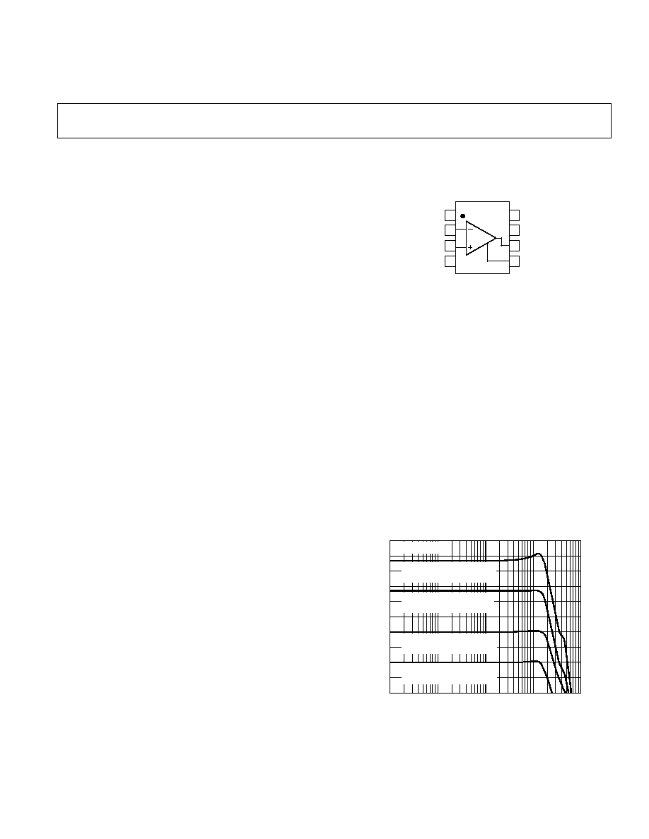
FREQUENCY Hz
0.1M
1G
1M
10M
100M
CLOSED LOOP GAIN dB
24
21
6
18
15
12
9
6
3
0
3
V
OUT
= 50mV p-p
G = 5, R
F
= 1k , R
G
= 200 ,
R
IN
= 66.5 , C
C
= 1.5pF
G = 2, R
F
=
499 , R
G
= 249 ,
R
IN
= 63.4 , C
C
= 4pF
G = 1, R
F
=
499 , R
G
= 499 ,
R
IN
= 56.2 , C
C
= 7pF
G = 10, R
F
=
1k , R
G
= 100 ,
R
IN
= 100 , C
C
= 0pF
Figure 1. Small Signal Frequency Response
CONNECTION DIAGRAM
SOIC-8 (R-8)
MICRO_SOIC-8 (RM-8)
8
7
6
5
1
2
3
4
LOGIC
REFERENCE
IN
+IN
V
S
DISABLE
+V
S
V
OUT
C
COMP
AD8021

REV. 0
2
AD8021SPECIFICATIONS
VS =
AD8021AR/ARM
Parameter
Conditions
Min
Typ
Max
Unit
DYNAMIC PERFORMANCE
3 dB Small Signal Bandwidth
G = +1, C
C
= 10 pF, V
O
= 0.05 V p-p
355
490
MHz
G = +2, C
C
= 7 pF, V
O
= 0.05 V p-p
160
205
MHz
G = +5, C
C
= 2 pF, V
O
= 0.05 V p-p
150
185
MHz
G = +10, C
C
= 0 pF, V
O
= 0.05 V p-p
110
150
MHz
Slew Rate, 1 V Step
G = +1, C
C
= 10 pF
95
120
V/
µ
s
G = +2, C
C
= 7 pF
120
150
V/
µ
s
G = +5, C
C
= 2 pF
250
300
V/
µ
s
G = +10, C
C
= 0 pF
380
420
V/
µ
s
Settling Time to 0.01%
V
O
= 1 V Step, R
L
= 500
23
ns
Overload Recovery (50%)
±
2.5 V Input Step, G = 2
50
ns
DISTORTION/NOISE PERFORMANCE
f = 1 MHz
HD2
V
O
= 2 V p-p
93
dBc
HD3
V
O
= 2 V p-p
108
dBc
f = 5 MHz
HD2
V
O
= 2 V p-p
70
dBc
HD3
V
O
= 2 V p-p
80
dBc
Input Voltage Noise
f = 50 kHz
2.1
2.6
nV/
Hz
Input Current Noise
f = 50 kHz
2.1
pA/
Hz
Differential Gain Error
NTSC, R
L
= 150
0.03
%
Differential Phase Error
NTSC, R
L
= 150
0.04
Degree
DC PERFORMANCE
Input Offset Voltage
0.4
1.0
mV
Input Offset Voltage Drift
T
MIN
T
MAX
0.5
µ
V/
°
C
Input Bias Current
+Input or Input
7.5
10.5
µ
A
Input Bias Current Drift
10
nA/
°
C
Input Offset Current
0.1
0.5
±µ
A
Open Loop Gain
82
86
dB
INPUT CHARACTERISTICS
Input Resistance
10
M
Common Mode Input Capacitance
1
pF
Input Common-Mode Voltage Range
5.3 to +5.0
V
Common-Mode Rejection Ratio
V
CM
=
±
4 V
86
98
dB
OUTPUT CHARACTERISTICS
Output Voltage Swing
3.5 to +3.2
3.8 to +3.4
V
Linear Output Current
60
mA
Short Circuit Current
75
mA
Capacitive Load Drive for 30% Overshoot
V
O
= 50 mV p-p/1 V p-p
15/120
pF
DISABLE CHARACTERISTICS
Off Isolation
f = 10 MHz
40
dB
Turn-On Time
V
O
= 0 V to 2 V, 50% Logic to
50% Output
45
ns
Turn-Off Time
V
O
= 0 V to 2 V, 50% Logic to
50% Output
50
ns
DISABLE Voltage--Off/On
V
DISABLE
V
LOGIC REFERENCE
1.75/1.90
V
Enabled Leakage Current
Logic Ref = 0.4 V
70
µ
A
DISABLE = 4.0 V
2
µ
A
Disabled Leakage Current
Logic Ref = 0.4 V
30
µ
A
DISABLE = 0.4 V
33
µ
A
POWER SUPPLY
Operating Range
±
2.25
±
5
±
12.0
V
Quiescent Current
Output Enabled
7.0
7.7
mA
Output Disabled
1.3
1.6
mA
+Power Supply Rejection Ratio
V
CC
= +4 V to +6 V, V
EE
= 5 V
86
95
dB
Power Supply Rejection Ratio
V
CC
= +5 V, V
EE
= 6 V to 4 V
86
95
dB
Specifications subject to change without notice.
(@ T
A
= 25 C, R
L
= 1 k
, Gain = +2, unless otherwise
noted.)
FOR
V
S
= 5 V

REV. 0
3
SPECIFICATIONS
FOR
V
S
= 12 V
VS =
(@ T
A
= 25 C, R
L
= 1 k , Gain = +2,
unless otherwise noted.)
AD8021AR/ARM
Parameter
Conditions
Min
Typ
Max
Unit
DYNAMIC PERFORMANCE
3 dB Small Signal Bandwidth
G = +1, C
C
= 10 pF, V
O
= 0.05 V p-p
520
560
MHz
G = +2, C
C
= 7 pF, V
O
= 0.05 V p-p
175
220
MHz
G = +5, C
C
= 2 pF, V
O
= 0.05 V p-p
170
200
MHz
G = +10, C
C
= 0 pF, V
O
= 0.05 V p-p
125
165
MHz
Slew Rate, 1 V Step
G = +1, C
C
= 10 pF
105
130
V/
µ
s
G = +2, C
C
= 7 pF
140
170
V/
µ
s
G = +5, C
C
= 2 pF
265
340
V/
µ
s
G = +10, C
C
= 0 pF
400
460
V/
µ
s
Settling Time to 0.01%
V
O
= 1 V Step, R
L
= 500
21
ns
Overload Recovery (50%)
±
6 V Input Step, G = 2
90
ns
DISTORTION/NOISE PERFORMANCE
f = 1 MHz
HD2
V
O
= 2 V p-p
95
dBc
HD3
V
O
= 2 V p-p
116
dBc
f = 5 MHz
HD2
V
O
= 2 V p-p
71
dBc
HD3
V
O
= 2 V p-p
83
dBc
Input Voltage Noise
f = 50 kHz
2.1
2.6
nV/
Hz
Input Current Noise
f = 50 kHz
2.1
pA/
Hz
Differential Gain Error
NTSC, R
L
= 150
0.03
%
Differential Phase Error
NTSC, R
L
= 150
0.04
Degree
DC PERFORMANCE
Input Offset Voltage
0.4
1.0
mV
Input Offset Voltage Drift
T
MIN
T
MAX
0.2
µ
V/
°
C
Input Bias Current
+Input or Input
8
11.3
µ
A
Input Bias Current Drift
10
nA/
°
C
Input Offset Current
0.1
0.5
±µ
A
Open Loop Gain
84
88
dB
INPUT CHARACTERISTICS
Input Resistance
10
M
Common-Mode Input Capacitance
1
pF
Input Common-Mode Voltage Range
12.2 to +12.0
V
Common-Mode Rejection Ratio
V
CM
=
±
10 V
86
96
dB
OUTPUT CHARACTERISTICS
Output Voltage Swing
10.2 to +9.8 10.6 to +10.2
V
Linear Output Current
70
mA
Short Circuit Current
115
mA
Capacitive Load Drive for 30% Overshoot
V
O
= 50 mV p-p/1 V p-p
15/120
pF
DISABLE CHARACTERISTICS
Off Isolation
f = 10 MHz
40
dB
Turn-On Time
V
O
= 0 V to 2 V, 50% Logic to
50% Output
45
ns
Turn-Off Time
V
O
= 0 V to 2 V, 50% Logic to
50% Output
50
ns
DISABLE Voltage--Off/On
V
DISABLE
V
LOGIC REFERENCE
1.80/1.95
V
Enabled Leakage Current
Logic Ref = 0.4 V
70
µ
A
DISABLE = 4.0 V
2
µ
A
Disabled Leakage Current
Logic Ref = 0.4 V
30
µ
A
DISABLE = 0.4 V
33
µ
A
POWER SUPPLY
Operating Range
±
2.25
±
5
±
12.0
V
Quiescent Current
Output Enabled
7.8
8.6
mA
Output Disabled
1.7
2.0
mA
+Power Supply Rejection Ratio
V
CC
= +11 V to +13 V, V
EE
= 12 V
86
96
dB
Power Supply Rejection Ratio
V
CC
= +12 V, V
EE
= 13 V to 11 V
86
100
dB
Specifications subject to change without notice.
AD8021

REV. 0
4
AD8021SPECIFICATIONS
VS =
AD8021AR/ARM
Parameter
Conditions
Min
Typ
Max
Unit
DYNAMIC PERFORMANCE
3 dB Small Signal Bandwidth
G = +1, C
C
= 10 pF, V
O
= 0.05 V p-p
270
305
MHz
G = +2, C
C
= 7 pF, V
O
= 0.05 V p-p
155
190
MHz
G = +5, C
C
= 2 pF, V
O
= 0.05 V p-p
135
165
MHz
G = +10, C
C
= 0 pF, V
O
= 0.05 V p-p
95
130
MHz
Slew Rate, 1 V Step
G = +1, C
C
= 10 pF
80
110
V/
µ
s
G = +2, C
C
= 7 pF
110
140
V/
µ
s
G = +5, C
C
= 2 pF
210
280
V/
µ
s
G = +10, C
C
= 0 pF
290
390
V/
µ
s
Settling Time to 0.01%
V
O
= 1 V Step, R
L
= 500
28
ns
Overload Recovery (50%)
0 V to 2.5 V Input Step, G = 2
40
ns
DISTORTION/NOISE PERFORMANCE
f = 1 MHz
HD2
V
O
= 2 V p-p
84
dBc
HD3
V
O
= 2 V p-p
91
dBc
f = 5 MHz
HD2
V
O
= 2 V p-p
68
dBc
HD3
V
O
= 2 V p-p
81
dBc
Input Voltage Noise
f = 50 kHz
2.1
2.6
nV/
Hz
Input Current Noise
f = 50 kHz
2.1
pA/
Hz
DC PERFORMANCE
Input Offset Voltage
0.4
1.0
mV
Input Offset Voltage Drift
T
MIN
T
MAX
0.8
µ
V/
°
C
Input Bias Current
+Input or Input
7.5
10.3
µ
A
Input Bias Current Drift
10
nA/
°
C
Input Offset Current
0.1
0.5
±µ
A
Open Loop Gain
72
76
dB
INPUT CHARACTERISTICS
Input Resistance
10
M
Common-Mode Input Capacitance
1
pF
Input Common-Mode Voltage Range
0.6 to 5.1
V
Common-Mode Rejection Ratio
1.5 V to 3.5 V
84
98
dB
OUTPUT CHARACTERISTICS
Output Voltage Swing
1.25 to 3.38
1.10 to 3.60
V
Linear Output Current
30
mA
Short Circuit Current
50
mA
Capacitive Load Drive for 30% Overshoot
V
O
= 50 mV p-p/1 V p-p
10/120
pF
DISABLE CHARACTERISTICS
Off Isolation
f = 10 MHz
40
dB
Turn-On Time
V
O
= 0 V to 1 V, 50% Logic to
50% Output
45
ns
Turn-Off Time
V
O
= 0 V to 1 V, 50% Logic to
50% Output
50
ns
DISABLE Voltage--Off/On
V
DISABLE
V
LOGIC REFERENCE
1.55/1.70
V
Enabled Leakage Current
Logic Ref = 0.4 V
70
µ
A
DISABLE = 4.0 V
2
µ
A
Disabled Leakage Current
Logic Ref = 0.4 V
30
µ
A
DISABLE = 0.4 V
33
µ
A
POWER SUPPLY
Operating Range
±
2.25
±
5
±
12.0
V
Quiescent Current
Output Enabled
6.7
7.5
mA
Output Disabled
1.2
1.5
mA
+Power Supply Rejection Ratio
V
CC
= +4.5 V to +5.5 V, V
EE
= 0 V
74
82
dB
Power Supply Rejection Ratio
V
CC
= +5 V, V
EE
= 0.5 V to +0.5 V
76
84
dB
Specifications subject to change without notice.
(@ T
A
= 25 C, R
L
= 1 k
, Gain = +2, unless otherwise
noted.)
FOR
V
S
= +5 V
REV. 0
AD8021
5
CAUTION
ESD (electrostatic discharge) sensitive device. Electrostatic charges as high as 4000 V readily
accumulate on the human body and test equipment and can discharge without detection. Although
the AD8021 features proprietary ESD protection circuitry, permanent damage may occur on
devices subjected to high-energy electrostatic discharges. Therefore, proper ESD precautions are
recommended to avoid performance degradation or loss of functionality.
WARNING!
ESD SENSITIVE DEVICE
ABSOLUTE MAXIMUM RATINGS
1
Supply Voltage . . . . . . . . . . . . . . . . . . . . . . . . . . . . . . . 26.4 V
Power Dissipation . . . . . . . . . Observe Power Derating Curves
Input Voltage (Common-Mode) . . . . . . . . . . . . . . .
±
V
S
±
1 V
Differential Input Voltage
2
. . . . . . . . . . . . . . . . . . . . . .
±
0.8 V
Differential Input Current . . . . . . . . . . . . . . . . . . . . . .
±
10 mA
Output Short Circuit Duration
. . . . . . . . . . . . . . . . . . . Observed Power Derating Curves
Storage Temperature . . . . . . . . . . . . . . . . . . 65
°
C to +125
°
C
Operating Temperature Range . . . . . . . . . . . 40
°
C to +85
°
C
Lead Temperature Range (Soldering, 10 sec) . . . . . . . . 300
°
C
NOTES
1
Stresses above those listed under Absolute Maximum Ratings may cause perma-
nent damage to the device. This is a stress rating only and functional operation of
the device at these or any other conditions above those indicated in the operational
section of this specification is not implied. Exposure to absolute maximum rating
conditions for extended periods may affect device reliability.
2
The AD8021 inputs are protected by diodes. Current-limiting resistors are not
used in order to preserve the low noise. If a differential input exceeds
±
0.8 V, the
input current should be limited to
±
10 mA.
MAXIMUM POWER DISSIPATION
The maximum power that can be safely dissipated by the AD8021
is limited by the associated rise in junction temperature. The
maximum safe junction temperature for plastic encapsulated
devices is determined by the glass transition temperature of the
plastic, approximately 150
°
C. Temporarily exceeding this limit
may cause a shift in parametric performance due to a change in
the stresses exerted on the die by the package. Exceeding a junc-
tion temperature of 175
°
C for an extended period can result in
device failure.
While the AD8021 is internally short circuit protected, this
may not be sufficient to guarantee that the maximum junction
temperature (150
°
C) is not exceeded under all conditions. To
ensure proper operation, it is necessary to observe the maximum
power derating curves.
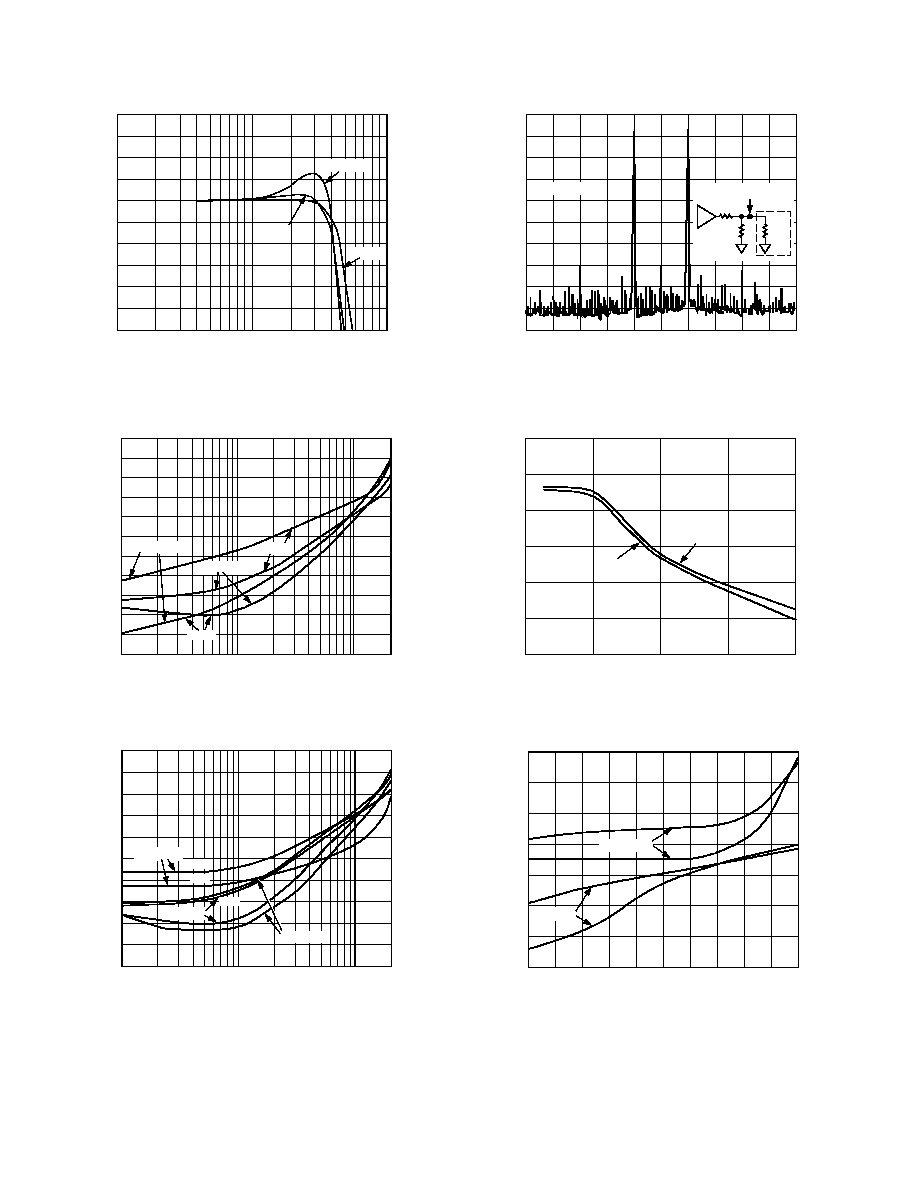
PIN FUNCTION DESCRIPTIONS
Pin No.
Mnemonic
Function
1
Logic Reference
Reference for Pin 8
*
Voltage Level. Connect to
Logic Low Supply
2
IN
Inverting Input
3
+IN
Noninverting Input
4
V
S
Negative Supply Voltage
5
C
COMP
Compensation Capacitor. Tie
to V
S
. (See the Applications
section for value.)
6
V
OUT
Output
7
+V
S
Positive Supply Voltage
8
DISABLE
Disable, Active Low
*
*When Pin 8 (DISABLE) is about two or more volts higher than Pin 1 (LOGIC
REFERENCE), the part is enabled. When Pin 8 is brought down to within about 1.5
volts of Pin 1, the part is disabled. (See the specification tables for exact disable and
enable voltage levels.) If the disable feature is not going to be used, Pin 8 can be tied
to +V
S
or a logic high source, and Pin 1 can be tied to ground or logic low. Alterna-
tively, if Pin 1 and Pin 8 are not connected, the part will be in an enabled state.
ORDERING GUIDE
Model
Temperature Range
Package Description
Package Outline
Branding Information
AD8021AR
40
°
C to +85
°
C
8-Lead SOIC
SO-8
AD8021AR-REEL
40
°
C to +85
°
C
8-Lead SOIC
SO-8
AD8021AR-REEL7
40
°
C to +85
°
C
8-Lead SOIC
SO-8
AD8021ARM
40
°
C to +85
°
C
8-Lead MICRO_SOIC
RM-8
HNA
AD8021ARM-REEL
40
°
C to +85
°
C
8-Lead MICRO_SOIC
RM-8
HNA
AD8021ARM-REEL7
40
°
C to +85
°
C
8-Lead MICRO_SOIC
RM-8
HNA
AD8021AR-EVAL
Evaluation Board
SO-8
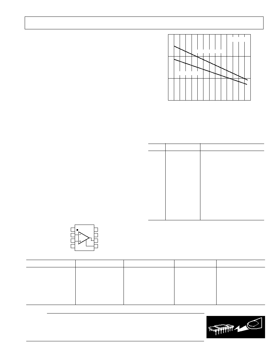
AMBIENT TEMPERATURE C
1.5
1.0
0
50
80
40
PO
WER DISSIP
A
TION
W
30 20 10
0
10
20
30
40
50
60
70
0.5
90
8-LEAD SOIC
8-LEAD SOIC PACKAGE
T
J
= 150 C
Figure 2. Maximum Power Dissipation vs. Temperature*
*Specification is for device in free air:
8-Lead SOIC:
JA
= 160
°
C/W
8-Lead MICRO_SOIC:
JA
= 200
°
C/W
PIN CONFIGURATION
8
7
6
5
1
2
3
4
LOGIC
REFERENCE
IN
+IN
V
S
DISABLE
+V
S
V
OUT
C
COMP
AD8021
REV. 0
AD8021
6
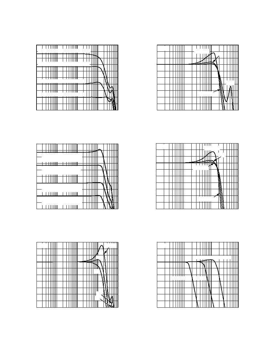
Typical Performance Characteristics
(T
A
= 25 C, V
S
= 5 V, R
L
= 1 k , G = +2, R
F
= R
G
= 499 , R
S
= 49.9 , R
O
= 976 , R
D
= 53.6 , C
C
= 7 pF, C
L
= 0, C
F
= 0, V
OUT
= 2 V p-p,
Freq = 1 MHz, except as otherwise noted.)
FREQUENCY Hz
0.1M
1G
1M
10M
100M
CLOSED-LOOP GAIN
dB
24
21
6
18
15
12
9
6
3
0
3
G = +1, R
F
= 75 , C
C
= 10pF
G = +5, R
F
=
1k , R
G
= 249 , C
C
= 2pF
G = +10, R
F
=
1k , R
G
= 110 , C
C
= 0pF
G = +2, R
F
=
R
G
= 499 , C
C
= 7pF
TPC 1. Small Signal Frequency Response vs.
Frequency and Gain, V
OUT
= 50 mV p-p, Nonin-
verting. See Test Circuit 1.
FREQUENCY Hz
0.1M
1G
1M
10M
100M
GAIN
dB
24
21
6
18
15
12
9
6
3
0
3
G = 5, R
F
= 1k , R
G
= 200 ,
R
IN
= 66.5 , C
C
= 1.5pF
G = 2, R
F
=
499 , R
G
= 249 ,
R
IN
= 63.4 , C
C
= 4pF
G = 1, R
F
=
499 , R
G
= 499 ,
R
IN
= 56.2 , C
C
= 7pF
G = 10, R
F
=
1k , R
G
= 100 ,
R
IN
= 100 , C
C
= 0pF
TPC 2. Small Signal Frequency Response vs.
Frequency and Gain, V
OUT
= 50 mV p-p, Invert-
ing. See Test Circuit 1.
FREQUENCY Hz
0.1M
1G
1M
GAIN
dB
10M
100M
9
8
1
7
6
5
4
3
2
1
0
G = +2
C
C
= 5pF
7pF
7pF
9pF
9pF
TPC 3. Small Signal Frequency Response vs.
Frequency and Compensation Capacitor, V
OUT
= 50 mV p-p. See Test Circuit 1.
FREQUENCY Hz
1G
1M
GAIN
dB
10M
100M
9
8
1
7
6
5
4
3
2
1
0
G = +2
V
S
= 2.5V
5V
V
S
= 2.5V
12V
TPC 4. Small Signal Frequency Response vs.
Frequency and Supply, V
OUT
= 50 mV p-p, Non-
inverting. See Test Circuit 1.
FREQUENCY Hz
1G
1M
GAIN
dB
10M
100M
3
2
7
1
0
1
2
3
4
5
6
G = 1
V
S
= 2.5V
5V
V
S
= 2.5V
V
S
= 12V
TPC 5. Small Signal Frequency Response vs.
Frequency and Supply, V
OUT
= 50 mV p-p,
Inverting. See Test Circuit 3.
FREQUENCY Hz
1G
1M
GAIN
dB
10M
100M
9
8
1
7
6
5
4
3
2
1
0
G = +2
V
OUT
= 0.1V AND 50mV p-p
V
OUT
= 4V p-p
1V p-p
TPC 6. Frequency Response vs. Frequency
and V
OUT
, Noninverting. See Test Circuit 1.
REV. 0
AD8021
7
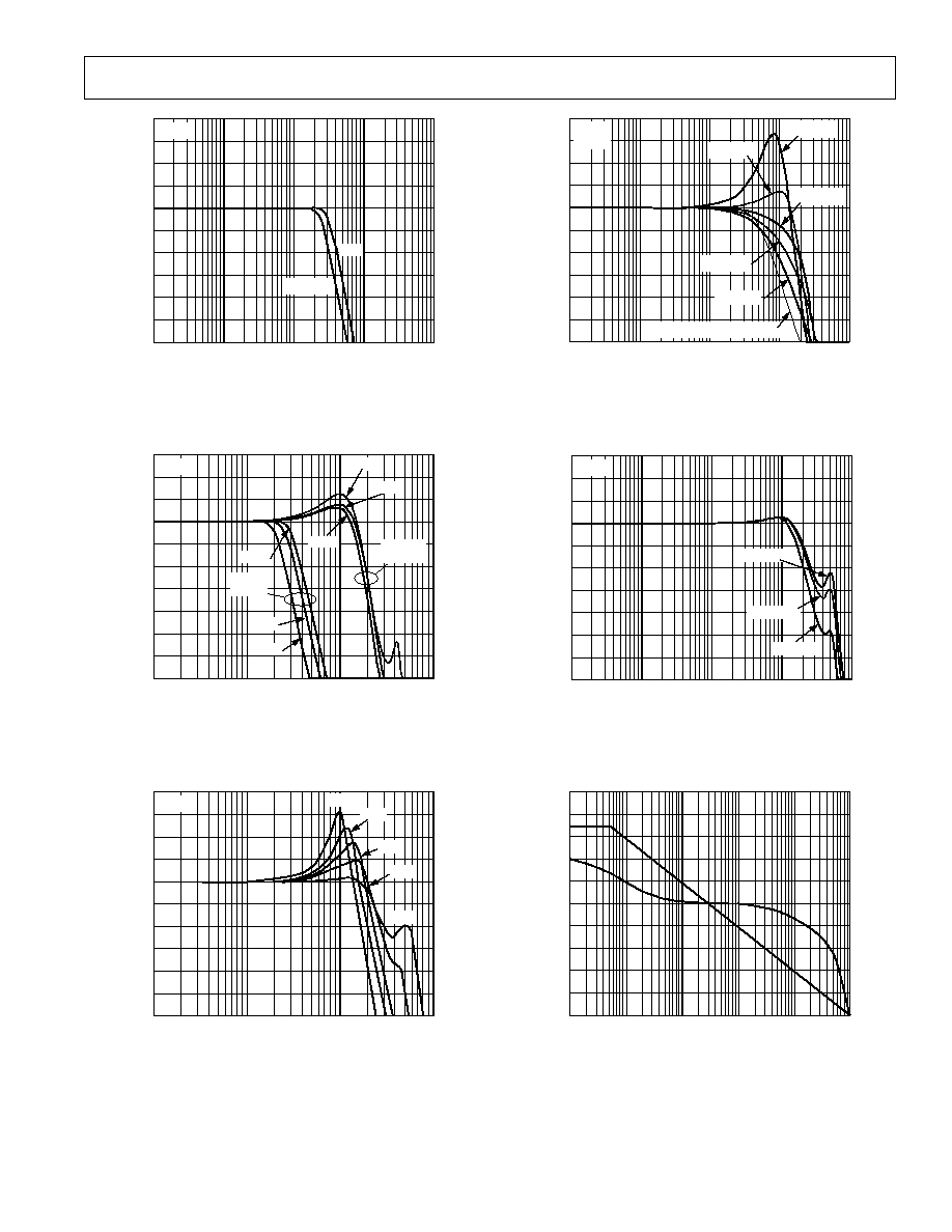
FREQUENCY Hz
0.1M
1G
1M
GAIN
dB
10M
100M
9
8
7
6
5
4
3
2
1
0
G = +2
R
L
= 100
1k
10
TPC 7. Large Signal Frequency Response vs.
Frequency and Load, Noninverting. See Test
Circuit 2.
FREQUENCY Hz
1G
1M
GAIN
dB
10M
100M
9
8
7
6
5
4
3
2
1
0
G = +2
+85 C
V
OUT
=
50mV p-p
40 C
+25 C
+85 C
40 C
+25 C
1
V
OUT
=
2V p-p
TPC 8. Frequency Response vs. Frequency
Temperature and V
OUT
, Noninverting. See
Test Circuit 1.
FREQUENCY Hz
1G
1M
GAIN
dB
10M
100M
15
12
9
6
3
0
3
6
9
12
G = +2
18
50pF
30pF
20pF
10pF
0pF
TPC 9. Small Signal Frequency Response vs.
Frequency and Capacitive Load, Nonin
vert-
ing, V
OUT
= 50 mV p-p. See Test Circuit 2 and
Figure 16.
FREQUENCY Hz
1G
0.1M
10M
100M
GAIN
dB
9
8
7
6
5
4
3
2
1
0
G = +2
R
F
= R
G
10
R
F
= 1k
R
F
= 499
R
F
= 250
R
F
= 150
R
F
= 75
R
F
= 1k AND C
F
= 2.2pF
1M
TPC 10. Small Signal Frequency Response
vs. Frequency and R
F
, Noninverting, V
OUT
=
50 mV p-p. See Test Circuit 1.
FREQUENCY Hz
0.1M
1G
1M
GAIN
dB
10M
100M
12
9
6
3
0
3
6
9
12
15
G = +2
R
S
= 49.9
15
R
S
= 100
R
S
= 249
TPC 11. Small Signal Frequency Response
vs. Frequency and R
S
, Noninverting. V
OUT
=
50 mV p-p. See Test Circuit 1.
FREQUENCY Hz
100k
1G
1M
OPEN-LOOP GAIN
dB
10M
100M
100
90
80
70
60
50
40
30
20
10
0
PHASE
Degrees
90
45
0
45
90
135
135
180
10k
TPC 12. Open-Loop Gain and Phase vs.
Frequency. R
G
=100
, R
F
= 1 k
, R
O
= 976
,
R
D
= 53.6, C
C
= 0 pF. See Test Circuit 3.
REV. 0
AD8021
8
FREQUENCY Hz
1M
GAIN
dB
10M
100M
6.2
6.0
5.8
5.6
5.4
G = +2
6.4
V
S
= 2.5V
5V
12V
TPC 13. 0.1 dB Flatness vs. Frequency and Sup-
ply, V
OUT
= 1 V p-p, R
L
= 150
. Noninverting, See
Test Circuit 2.
FREQUENCY Hz
0.1M
DIST
O
R
T
ION
dBc
1M
40
60
90
110
130
20
30
50
70
80
100
120
10M
R
L
= 100
R
L
= 1k
3RD
2ND
20M
TPC 14. Second and Third Harmonic Distortion vs.
Frequency and R
L
FREQUENCY Hz
100k
DIST
O
R
T
ION
dBc
1M
20M
40
60
90
110
130
30
50
70
80
100
120
10M
V
S
= 2.5V
2ND
3RD
V
S
= 12V
V
S
= 5V
3RD
3RD
2ND
2ND
TPC 15. Second and Third Harmonic Distortion vs.
Frequency and V
S
8
FREQUENCY MHz
9.5
P
OUT
dBm
10
10.5
40
60
90
110
30
50
70
80
100
120
20
9.7
10.3
f =
0.2MHz
f
1
f
2
976
53.6
50
P
OUT
TPC 16. Intermodulation Distortion vs. Frequency
FREQUENCY MHz
0
THIRD ORDER INTERCEPT
dBm
10
20
45
30
25
40
35
20
50
5
15
V
S
= 5V
V
S
= 2.5V
TPC 17. Third Order Intercept vs. Frequency and
Supply Voltage
V
OUT
V p-p
1
DIST
O
R
T
ION
dBc
3
5
60
90
100
70
80
120
50
2
4
2ND
6
110
3RD
2ND
3RD
R
L
= 1k
R
L
= 100
TPC 18. Second and Third Harmonic Distortion vs.
V
OUT
and R
L
REV. 0
AD8021
9
V
OUT
V p-p
1
DIST
O
R
T
ION
dBc
3
5
60
90
100
70
80
120
50
2
4
2ND
6
110
3RD
2ND
3RD
f
C
= 1MHz
f
C
= 5MHz
TPC 19. Second and Third Harmonic Distortion
vs. V
OUT
and Fundamental Frequency (f
C
), G = +2
V
OUT
V p-p
1
DIST
O
R
T
ION
dBc
3
5
60
90
100
70
80
50
2
4
2ND
6
110
3RD
2ND
3RD
f
C
= 5MHz
f
C
= 1MHz
40
TPC 20. Second and Third Harmonic Distortion vs.
V
OUT
and Fundamental Frequency (f
C
), G = +10
FEEDBACK RESISTANCE
0
DIST
O
R
T
ION
dBc
400
800
90
110
80
200
600
2ND
1000
120
3RD
70
100
f
C
= 1MHz
R
L
= 1k
TPC 21. Second and Third Harmonic Distortion vs.
Feedback Resistor (R
F
)
LOAD
0
POSITIVE OUTPUT
V
O
L
T
A
GE
V
800
1600
3.2
2.9
3.4
400
1200
2000
2.8
3.5
3.1
3.3
3.0
NEGA
TIVE OUTPUT
V
O
L
T
A
GE
V
3.4
3.7
3.2
3.8
3.1
3.5
3.3
3.6
NEGATIVE OUTPUT
POSITIVE OUTPUT
TPC 22. DC Output Voltage vs. Load. See Test
Circuit 1.
TEMPERATURE C
50
10
30
30
10
50
70
90
110
60
0
100
120
40
80
20
V
S
=
2.5
V
S
= 5.0
V
S
= 12
SHOR
T
-
CIRCUIT CURRENT
mA
TPC 23. Short-Circuit Current to Ground vs.
Temperature
R
L
= 1k , 150
V
OUT
mV
50
40
30
20
10
10
20
30
40
50
G = +2
0
40
80
120
160
200
TIME ns
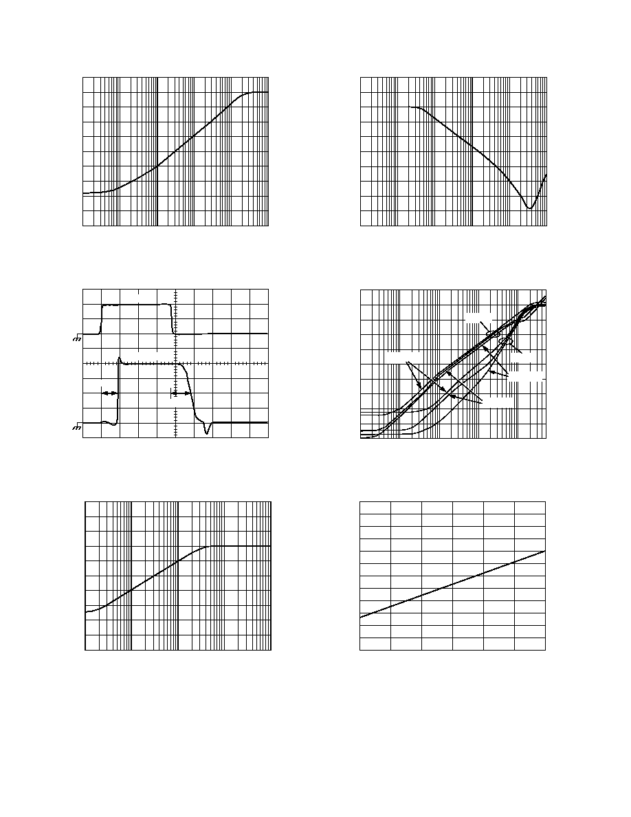
TPC 24. Small Signal Transient Response vs.
R
L
, V
O
= 50 mV p-p. See Test Circuit 2, Non-
inverting.
REV. 0
10
AD8021
V
O
= 4V p-p
G = +2
R
L
= 1k
R
L
= 150
V
OUT
V
2.0
1.0
1.0
2.0
0
40
80
120
160
200
TIME ns
TPC 25. Large Signal Transient Response vs. R
L
.
See Test Circuit 2, Noninverting.
V
O
= 4V p-p
G = 1
V
OUT
V
IN
5
4
3
2
1
1
2
3
4
5
VO
L
T
S
0
50
100
150
200
250
TIME ns
TPC 26. Large Signal Transient Response. See Test
Circuit 3, Inverting.
2.0
1.0
1.0
2.0
V
OUT
V
V
O
= 4V p-p
C
L
= 50pF
G = +2
C
L
= 10pF, 0pF
0
40
80
120
160
200
TIME ns
TPC 27. Large Signal Transient Response vs. C
L
.
See Test Circuit 1.
10
V
O
= 2V p-p
G = +2
V
S
= 5V
V
S
= 2.5V
V
OUT
V
2.0
1.0
1.0
2.0
0
40
80
120
160
200
TIME ns
TPC 28. Large Signal Transient Response vs. V
S
.
See Test Circuit 1.
V
IN
= 3V
G = +2
V
OUT,
R
L
= 1k
V
IN
= 1V/DIV
V
OUT
= 2V/DIV
V
IN
R
L
= 150
0
100
200
300
400
500
TIME ns
TPC 29. Overdrive Recovery vs. R
L
. See Test Circuit 2.
25ns
0.01%
+0.01%
HOR = 5ns/DIV
VERT = 0.2mV/DIV
G = +2
OUTPUT SETTLING
TPC 30. 0.01% Settling Time, 2 V Step
REV. 0
AD8021
11
G = +1
50
40
30
20
10
10
20
30
40
50
0
40
80
120
160
200
TIME ns
V
OUT
mV
TPC 31. Small Signal Transient Response,
V
O
= 50 mV p-p
. G = +1. See Test Circuit 1.
10M
FREQUENCY Hz
100
10
1
10
100
1k
10k
100k
1M
V
O
L
T
A
GE NOISE
nV/ Hz
2.1nV/ Hz
TPC 32. Input Voltage Noise vs. Frequency
FREQUENCY Hz
100
10M
1k
INPUT CURRENT NOISE
pA/ Hz
10k
100k
100
1
10
10
1M
TPC 33. Input Current Noise vs. Frequency
TEMPERATURE C
25
100
25
V
O
L
T
A
GE OFFSET
mV
50
75
0.48
0.24
50
0
0.44
0.40
0.36
0.32
0.28
TPC 34. V
OS
vs. Temperature
TEMPERATURE C
25
100
25
INPUT BIAS CURRENT
A
50
75
8.4
6.0
50
0
8.0
7.6
7.2
6.8
6.4
TPC 35. Input Bias Current vs. Temperature
FREQUENCY Hz
100k
10M
CMRR
dB
100M
20
10k
1M
30
40
50
60
70
80
90
100
110
120
TPC 36. CMRR vs. Frequency. See Test Circuit 4.
REV. 0
AD8021
12
FREQUENCY Hz
100k
1G
10M
OUTPUT IMPED
ANCE
100M
300
10k
1M
100
30
10
3
1
0.3
0.1
0.03
0.01
0.003
TPC 37. Output Impedance vs. Frequency, Chip Enabled.
See Test Circuit 5.
DISABLE
t
DIS
= 50ns
V
OUTPUT
4V
2V
2V
1V
t
EN
= 45ns
0
100
200
300
400
500
TIME ns
TPC 38. Enable (t
EN
)/Disable (t
DIS
) Time vs. V
OUT
. See
Test Circuit 6.
FREQUENCY Hz
1M
1G
DISABLED ISOLA
T
ION
dB
100M
0
0.1M
10M
10
20
30
40
50
60
70
80
90
100
TPC 39. Input to Output Isolation, Chip Disabled. See
Test Circuit 7.
FREQUENCY Hz
100k
1G
OUTPUT IMPED
ANCE
10M
300k
10k
1M
100k
30k
10k
3k
1k
300
100
30
10
3
100M
TPC 40. Output Impedance vs. Frequency, Chip Disabled.
See Test Circuit 8.
FREQUENCY Hz
1M
500M
PSRR
dB
100M
0
10k
10M
10
30
50
70
80
100
100k
20
40
60
90
V
S
= 2.5V
V
S
= 5V
V
S
= 12V
+PSRR
PSRR
TPC 41. PSRR vs. Frequency and Supply Voltage. See
Test Circuits 9 and 10.
TEMPERATURE C
0
100
SUPPL
Y CURRENT
mA
50
8.5
50
25
8.0
7.5
7.0
6.5
6.0
5.5
75
25
TPC 42. Quiescent Supply Current vs. Temperature
REV. 0
AD8021
13
50
V
S
C
C
+V
S
5
R
S
R
O
R
D
R
F
C
F
R
G
49.9
R
IN
50 CABLE
50 CABLE
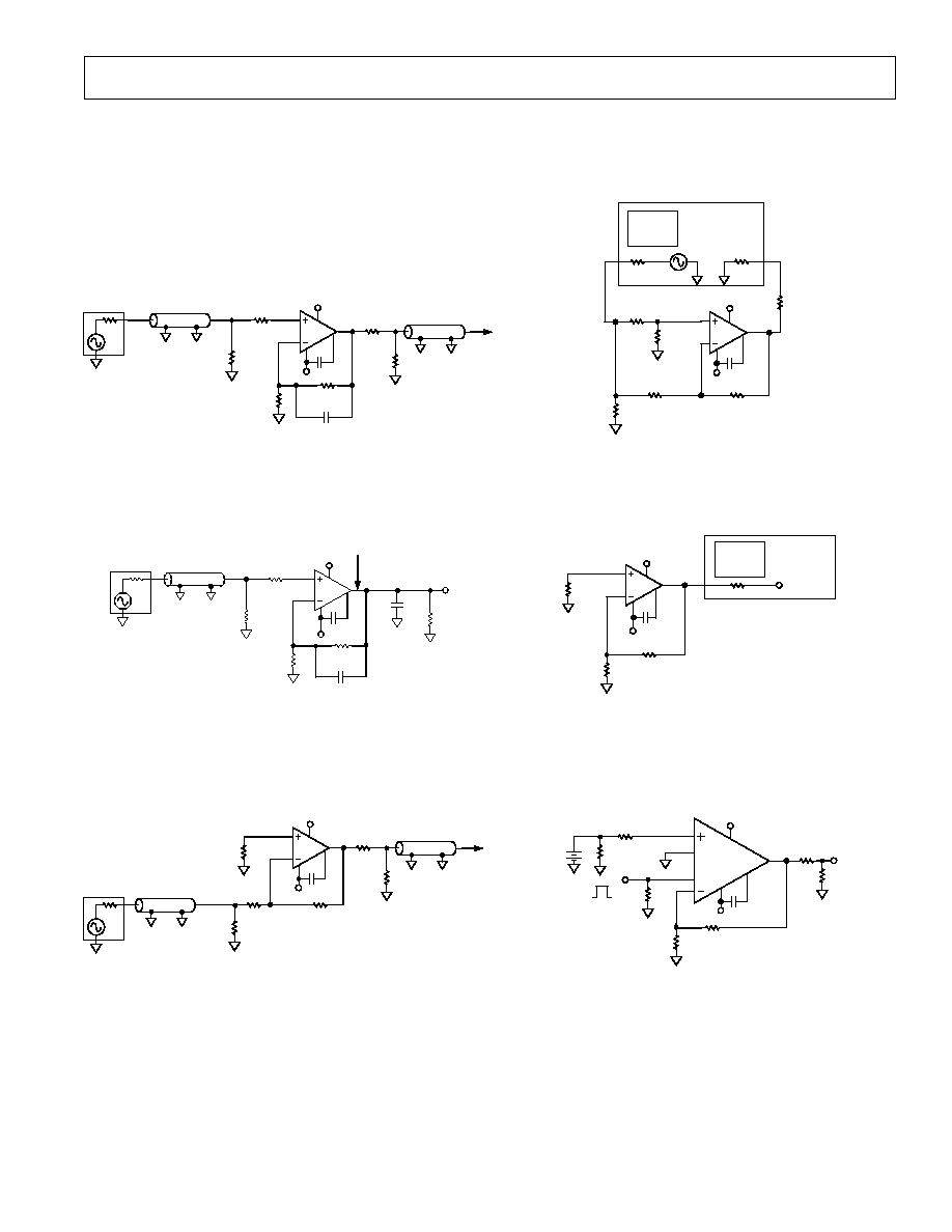
Test Circuit 1. Noninverting Gain Test Circuit
R
F
C
F
R
G
R
L
R
S
49.9
R
IN
C
C
C
L
FET
PROBE
50
V
S
+V
S
5
50
CABLE
Test Circuit 2. Noninverting Gain Test Circuit with FET
Probe
R
F
R
O
R
D
49.9
R
G
R
IN
49.9
50
V
S
C
C
+V
S
5
50
CABLE
50
CABLE
Test Circuit 3. Inverting Gain Test Circuit
TEST CIRCUITS
HP8753D
50
AD8021
499
499
55.6
499
499
49.9
NETWORK
ANALYZER
V
S
C
C
5
+V
S
7pF
50
Test Circuit 4. CMRR Test Circuit
AD8021
R
F
499
100
7pF
V
S
C
C
+V
S
5
NETWORK
ANALYZER
HP8753D
R
G
499
50
Test Circuit 5. Output Impedance, Chip Enabled
499
AD8021
49.9
49.9
7pF
V
S
C
C
5
976
1
8
1.0V
49.9
499
+V
S
DISABLE
LOGIC REF
4V
53.6
Test Circuit 6. Enable/Disable Test Circuit
REV. 0
AD8021
14
499
AD8021
49.9
49.9
V
S
C
C
7pF
5
1
8
499
NETWORK
ANALYZER
50
1k
FET
PROBE
+V
S
LOGIC REF
DISABLE
HP8753D
50
CABLE
50
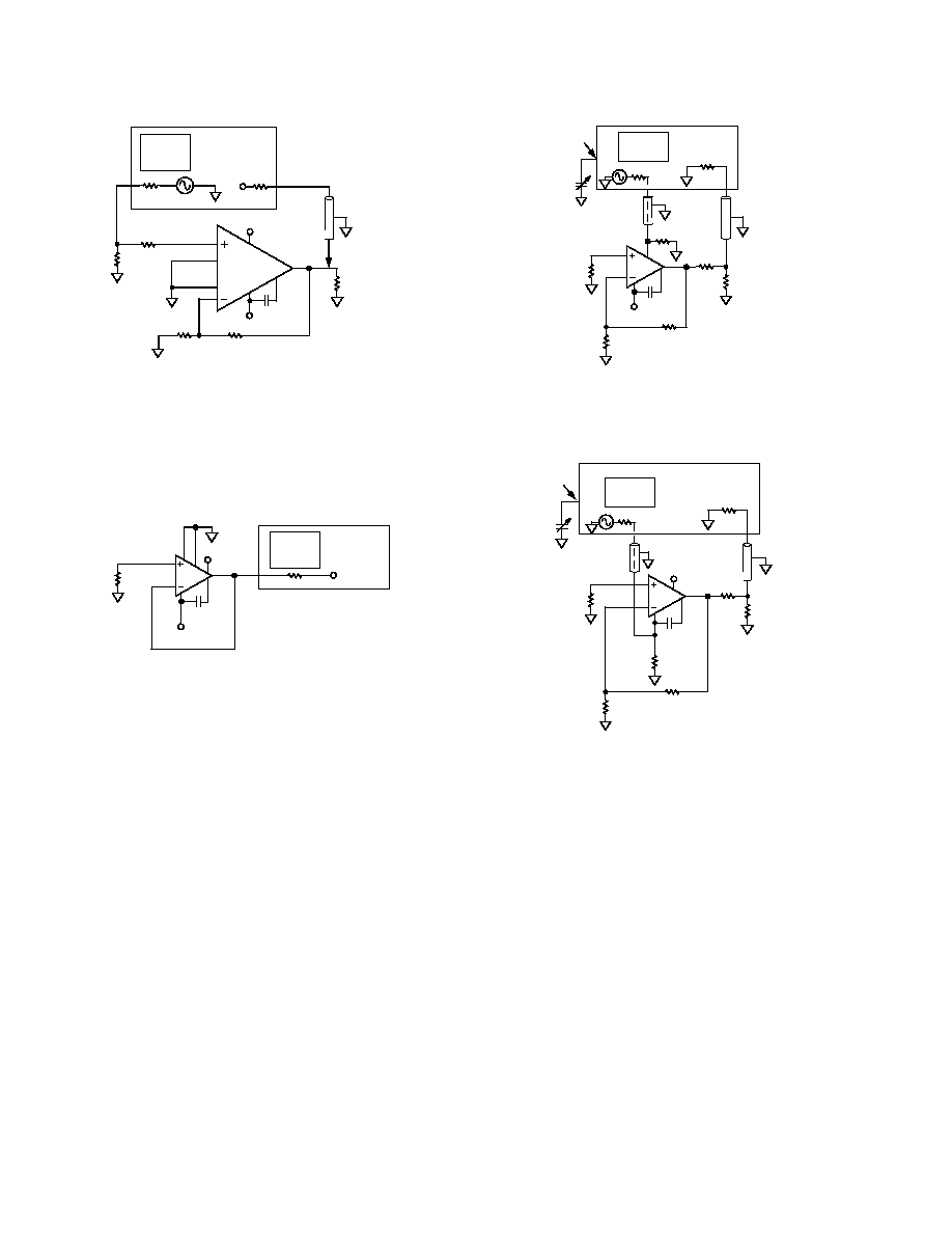
Test Circuit 7. Input to Output Isolation, Chip Disabled
+V
S
AD8021
100
1
8
NETWORK
ANALYZER
V
S
C
C
7pF
5
HP8753D
50
Test Circuit 8. Output Impedance, Chip Disabled
499
499
NETWORK
ANALYZER
249
976
53.6
49.9 , 5W
+V
S
50
V
S
C
C
7pF
5
HP8753D
+V
S
50
CABLE
BIAS
BNC
50
Test Circuit 9. Positive PSRR
+V
S
NETWORK
ANALYZER
50
249
976
499
499
53.6
V
S
49.9
5W
C
C
7pF
5
HP8753D
V
S
BIAS
BNC
50
CABLE
50
Test Circuit 10. Negative PSRR
REV. 0
AD8021
15
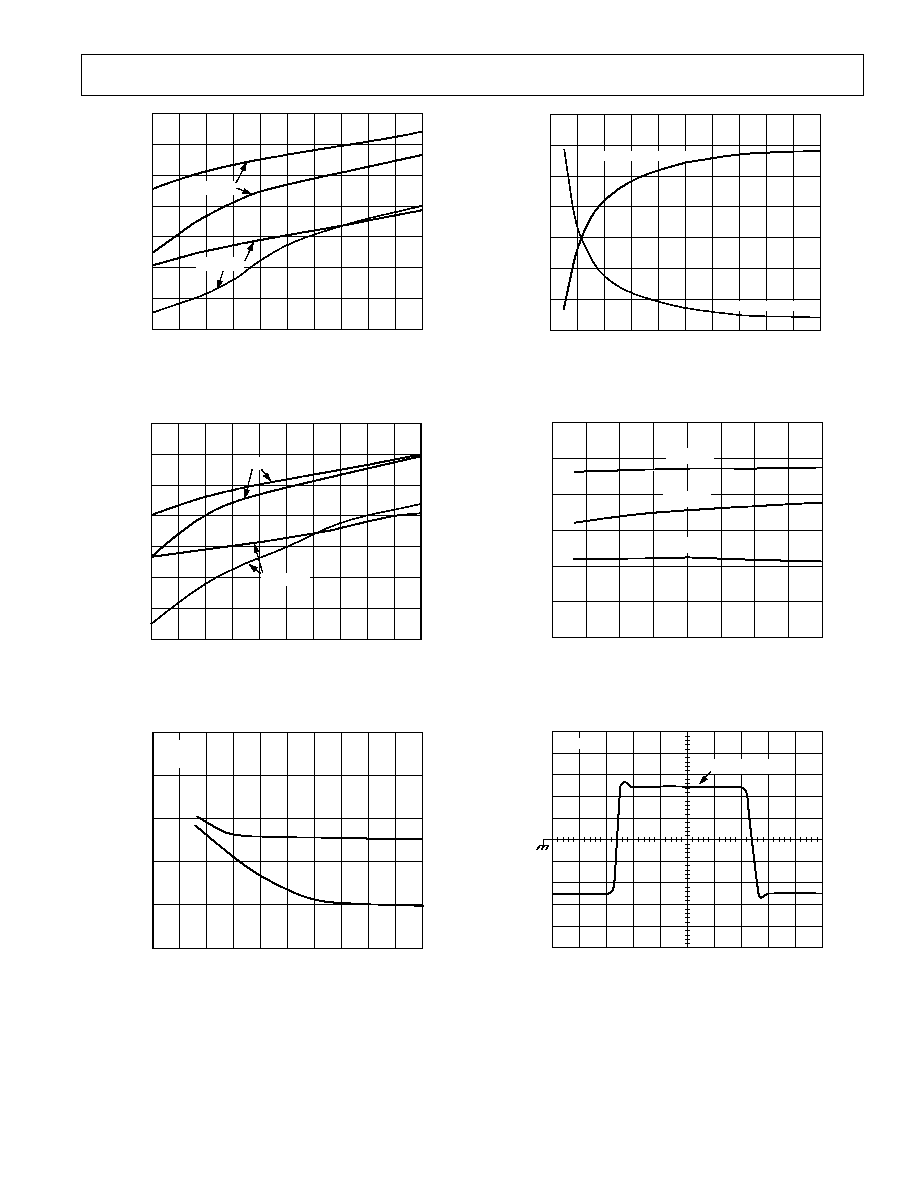
USING THE AD8021
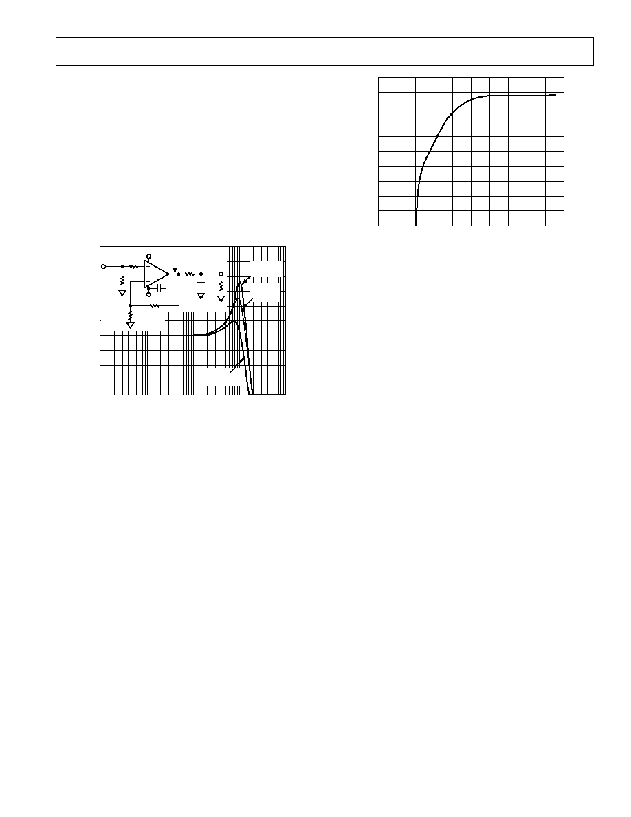
The typical voltage feedback op amp is frequency stabilized with
a fixed internal capacitor, C
INTERNAL
, using "dominant pole
compensation." To a first-order approximation, voltage feedback
op-amps have a fixed Gain Bandwidth Product; for example, if
its 3 dB bandwidth for G = +1 is 200 MHz, at a gain of G = +10,
its bandwidth will be only about 20 MHz. The AD8021 is a volt-
age feedback op amp with a minimal C
INTERNAL
of about 1.5 pF.
By adding an external compensation capacitor, C
C
, the user can
circumvent the fixed gain bandwidth limitation of other voltage
feedback op amps.
Unlike the typical op amp with fixed compensation, the AD8021
allows the user to:
1.
Maximize the amplifier bandwidth for closed-loop gains
between 1 and 10, avoiding the usual loss of bandwidth
and slew-rate.
2. Optimize the trade-off between bandwidth and phase
margin for a particular application.
3. Match bandwidth in gain blocks with different noise gains,
such as when designing differential amplifiers (as shown in
Figure 11 of the Applications section).
FREQUENCY Hz
1M
OPEN-LOOPGAIN
dB
100M
110
10k
10M
100
80
60
40
30
10
100k
90
70
50
20
C
C
= 10pF
1k
1G
10G
0
10
180
135
45
90
0
PHASE
Degrees
C
C
= 0pF
(B)
(C)
(A)
(A)
(B)
(C)
86
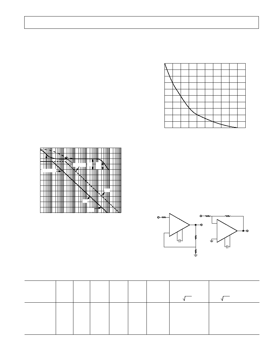
Figure 3. Simplified Diagram of AD8021 Open-Loop Gain
and Phase Response
Figure 3 is the AD8021 gain and phase plot that has been sim-
plified for instructional purposes. If the desired closed-loop gain
is G = +1, and C
C
= 10 pF is chosen, Arrow "A" of the figure
shows that the bandwidth is about 200 MHz and the phase
margin is about 60
°
. If the gain is changed to G = +10 and
C
C
fixed at 10 pF, then (as expected for a typical op amp), the
bandwidth is degraded to about 20 MHz, and the phase margin
increases to 90
°
(Arrow B). However, by reducing C
C
to zero, the
bandwidth and phase margin return to about 200 MHz and 60
°
(Arrow C), respectively. In addition, the slew rate is dramatically
increased, as it roughly varies with the inverse of C
C
.
1
2
3
4
5
6
7
8
9
10
11
1
2
3
4
5
6
7
8
9
10
0
NOISE GAIN V/V
COMPENSA
TION CAP
A
CIT
ANCE
pF
Figure 4. Suggested Compensation Capacitance vs. Gain
for Maintaining 1 dB Peaking
Table I and Figure 4 provide lists recommended values of com-
pensation capacitance at various gains, and the corresponding
slew rate, bandwidth, and noise. Note that the value of the
compensation capacitor depends on the circuit noise gain, not
voltage gain. As shown in Figure 5, the noise gain, G
N
, of an op
amp gain block is equal to its noninverting voltage gain, regard-
less of whether it is actually used for inverting or noninverting
gain. Thus,
Noninverting G
N
= R
F
/R
G
+1
Inverting G
N
= R
F
/R
G
+1
AD8021
C
COMP
3
2
V
S
5
6
R
F
800
R
G
200
+
G
= G
N
= 5
AD8021
C
COMP
2
3
V
S
5
6
+
G
= 4
G
N
= 5
R
F
800
R
G
200
R
S
NONINVERTING
INVERTING
1
Figure 5. The Noise Gain of Both Is Five
Table I. Recommended Component Values. See Test Circuit 2. C
F
= C
L
= 0, R
L
= 1 k , R
IN
= 49.9
Output
Output
Noise Gain
Slew
3 dB
Noise
Noise
(Noninverting
R
S
R
F
R
G
C
COMP
Rate
SS BW
(AD8021 Only)
(AD8021 with Resistors)
Gain)
( )
( )
( )
(pF)
(V/ s)
(MHz)
(nV/ )
(nV/ )
1
75
75
NA
10
120
490
2.1
2.8
2
49.9
499
499
7
150
205
4.3
8.2
5
49.9
1 k
249
2
300
185
10.7
15.5
10
49.9
1 k
110
0
420
150
21.2
27.9
20
49.9
1 k
52.3
0
200
42
42.2
52.7
100
49.9
1 k
10
0
34
6
211.1
264.1
Hz
Hz
REV. 0
AD8021
16
With the AD8021, a variety of trade-offs can be made to fine-
tune its dynamic performance. Sometimes more bandwidth or
slew rate is needed at a particular gain. Reducing the compen-
sation capacitance, as illustrated in TPC 3, will increase the
bandwidth and peaking due to a decrease in phase margin.
On the other hand, if more stability is needed, increasing the
compensation cap will decrease the bandwidth while increas-
ing the phase margin.
As with all high-speed amplifiers, parasitic capacitance and
inductance around the amplifier can affect its dynamic response.
Often the input capacitance (due to the op amp itself as well as
the pc board) could have a significant effect. The feedback resis-
tance, together with the input capacitance, may contribute to a loss
of phase margin, thereby affecting the high-frequency response,
as shown in TPC 10. As further shown, a capacitor (C
F
) in parallel
with the feedback resistor can compensate for this phase loss.
Additionally, any resistance in series with the source will
create a pole with the input capacitance (as well as dampen
high-frequency resonance due to package and board inductance
and capacitance), the effect of which is shown in TPC 11.
It must also be noted that increasing resistor values will increase
the overall noise of the amplifier, and that reducing the feedback
resistor value will increase the load on the output stage, thus
increasing distortion (TPC 18).
Using the Disable Feature
When Pin 8 (
DISABLE) is about two or more volts higher than
Pin 1 (LOGIC REFERENCE), the part is enabled. When Pin 8
is brought down to within about 1.5 volts of Pin 1, the part is
disabled. (See the specification tables for exact disable and
enable voltage levels). If the disable feature is not going to be
used, Pin 8 can be tied to +V
S
or a logic high source, and Pin 1
can be tied to ground or logic low. Alternatively, if Pin 1 and
Pin 8 are not connected, the part will be in an enabled state.
THEORY OF OPERATION
The AD8021 is fabricated on the second generation of Analog
Devices' proprietary High Voltage eXtra-Fast Complementary
Bipolar (XFCB) process, which enables the construction of PNP
and NPN transistors with similar f
T
's in the 3 GHz region. The
transistors are dielectrically isolated from the substrate (and
each other), eliminating the parasitic and latch-up problems
caused by junction isolation. It also reduces the nonlinear
capacitance (a source of distortion), and allows a higher tran-
sistor f
T
for a given quiescent current. The supply current is
trimmed, which results in less part-to-part variation of band-
width, slew rate, distortion, and settling time.
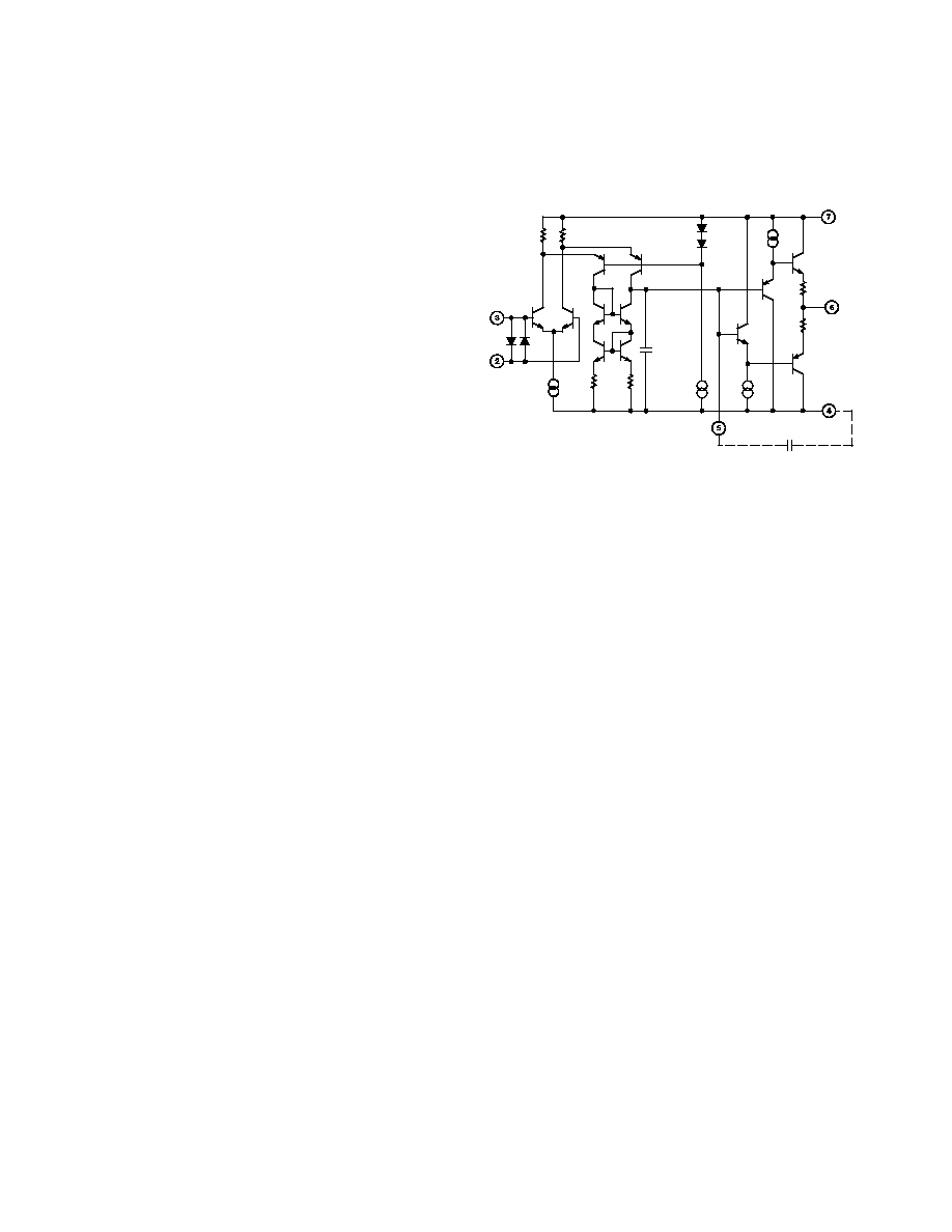
As shown in Figure 6, the AD8021 input stage consists of an NPN
differential pair in which each transistor operates at 0.8 mA collec-
tor current. This allows the input devices a high transconductance
and hence, the AD8021 has a low input noise of 2.1 nV/
Hz @
50 kHz. The input stage drives a folded cascode that consists of
a pair of PNP transistors. The folded cascode and current mirror
provide a differential to single-ended conversion of signal current.
This current then drives the high-impedance node (Pin 5), where
the C
C
external capacitor is connected. The output stage pre-
serves this high impedance with a current gain of 5,000, so that
the AD8021 can maintain a high open-loop gain, even when
driving heavy loads.
Two internal diode-clamps across the inputs (pins 2 and 3) protect
the input transistors from large voltages that could otherwise cause
emitter-base breakdown, which would result in degradation of
offset-voltage and input bias current.
C
C
OUTPUT
+V
S
V
S
+IN
IN
C
INTERNAL
1.5pF
C
COMP
Figure 6. Simplified Schematic
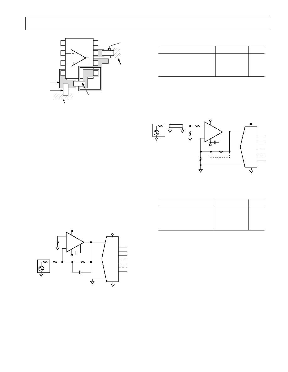
PCB LAYOUT CONSIDERATIONS
As with all high-speed op amps, achieving optimum performance
from the AD8021 requires careful attention to PC board layout.
Particular care must be exercised to minimize lead lengths
between the ground leads of the bypass capacitors and between
the compensation capacitor and the negative supply. Otherwise,
lead inductance can influence the frequency response and even
cause high frequency oscillations. Use of a multilayer printed
circuit board, with an internal ground plane, will reduce ground
noise and enable a compact component arrangement.
Due to the relatively high impedance of Pin 5, and low values of
the compensation capacitor, a guard ring is recommended. The
guard ring is simply a PC trace that encircles Pin 5 and is con-
nected to the output, Pin 6, which is at the same potential as Pin 5.
This serves two functions. It shields Pin 5 from any local circuit
noise generated by surrounding circuitry. It also minimizes stray
capacitance, which would tend to otherwise reduce the bandwidth.
An example of a guard ring layout may be seen in Figure 7.
Also shown in Figure 7, the compensation capacitor is located
immediately adjacent to the edge of the AD8021 package, span-
ning Pin 4 and Pin 5. This capacitor must be a high-quality
surface-mount COG or NPO ceramic. The use of leaded capaci-
tors is not recommended. The high-frequency bypass capacitor(s)
should be located immediately adjacent to the supplies, Pins 4 and 7.
To achieve the shortest possible lead length at the inverting input,
the feedback resistor R
F
is located beneath the board and just
spans the distance from the output, Pin 6, to inverting input Pin
2. The return node of resistor R
G
should be situated as closely as
possible to the return node of the negative supply bypass capacitor
connected to Pin 4.
REV. 0
AD8021
17
Table II. Summary of ADC Driver Performance,
f
C
= 65 kHz, V
OUT
= 10 V p-p
Parameter
Measurement
Unit
Second Harmonic Distortion
101.3
dB
Third Harmonic Distortion
109.5
dB
THD
100.0
dB
SFDR
100.3
dB
Figure 9 shows another ADC driver connection. The circuit was
tested with a noninverting gain of 10.1 and an output voltage of
approximately 20 V p-p, for optimum resolution and noise per-
formance. No filtering was used. An FFT was performed using
Analog Devices' evaluation software for the AD7665 16-bit con-
verter. The results are listed in Table III.
50
5V
AD8021
+
12V
+12V
AD7665
570 kSPS
16 BITS
50
3
2
R
F
750
OPTIONAL C
F
IN
LO
IN
6
50
HI
ADC
C
C
5
R
G
82.5
Figure 9. Noninverting ADC Driver, Gain = 10, f
C
= 100 kHz
Table III. Summary of ADC Driver Performance,
f
C
= 100 kHz, V
OUT
= 20 V p-p
Parameter
Measurement
Unit
Second Harmonic Distortion
92.6
dB
Third Harmonic Distortion
86.4
dB
THD
84.4
dB
SFDR
5.4
dB
DIFFERENTIAL DRIVER
The AD8021 is uniquely suited as a low-noise differential driver
for many ADCs, balanced lines, and other applications requir-
ing differential drive. If pairs of internally compensated op amps
are configured as inverter and follower, the noise gain of the
inverter will be higher than that of the follower section, result-
ing in an imbalance in the frequency response (see Figure 11).
A better solution takes advantage of the external compensation
feature of the AD8021. By reducing the C
COMP
value of the
inverter, its bandwidth may be increased to match that of the
follower, avoiding compromises in gain bandwidth and phase delay.
The inverting and noninverting bandwidths can be closely
matched using the compensation feature, thus minimizing
distortion.
DISABLE
V
OUT
8
7
6
1
2
3
LOGIC REFERENCE
IN
+IN
V
S
4
+V
S
5
BYPASS
CAPACITOR
GROUND
PLANE
COMPENSATION
CAPACITOR
GROUND
PLANE
(TOP VIEW)
BYPASS
CAPACITOR
METAL
C
COMP
Figure 7. Recommended Location of Critical Components
and Guard Ring
DRIVING 16-BIT ADC CONVERTERS
Low noise and adjustable compensation make the AD8021
especially suitable as a buffer/driver for high-resolution A-to-D
converters.
As seen in TPC 15, the harmonic distortion is better than
90 dB at frequencies between 100 kHz and 1 MHz. This is a
real advantage for complex waveforms that contain high-
frequency information, as the phase and gain integrity of the
sampled waveform can be preserved throughout the conversion
process. The increase in loop gain results in improved output
regulation and lower noise when the converter input changes
state during a `sample.' This advantage is particularly appar-
ent when using 16-bit high-resolution A-to-D converters, with
high sampling rates.
Figure 8 shows a typical ADC driver configuration. The
AD8021 is in an inverting gain of 7.5, f
C
is 65 kHz, and its
output voltage is 10 V p-p. The results are listed in Table II.
50
5V
AD8021
+
12V
+12V
AD7665
570 kSPS
16 BITS
590
3
2
R
F
1.5k
IN
LO
IN
6
HI
C
C
5
10pF
56pF
R
G
200
65kHz
Figure 8. Inverting ADC Driver, Gain = 7.5, f
C
= 65 kHz
REV. 0
AD8021
18
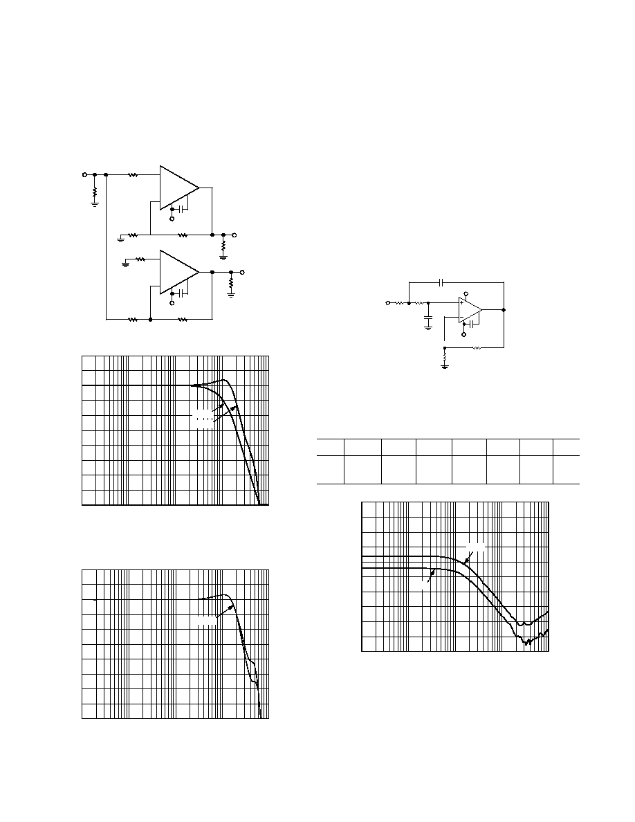
Figure 10 illustrates an inverter-follower driver circuit operating
at a gain of two, using individually compensated AD8021s. The
values of feedback and load resistors were selected to provide a
total load of less than 1 k
, and the equivalent resistances seen
at each op amp's inputs were matched in order to minimize
offset voltage and drift. Figure 12 is a plot of the resulting ac
responses of driver halves.
AD8021
+
3
2
6
7pF
249
499
G = +2
499
49.9
1k
V
OUT1
5
V
S
AD8021
+
3
2
6
5pF
232
G = 2
664
1k
V
OUT2
5
V
S
332
V
IN
Figure 10. Differential Amplifier
G = 2
G = +2
GAIN
dB
FREQUENCY Hz
100k
1M
10M
100M
1G
12
9
6
3
0
3
6
9
12
15
18
Figure 11. AC Response of Two Identically Compensated
High-Speed Op Amps Configured for Gain of +2 and 2
G = 2
100k
1M
10M
100M
1G
FREQUENCY Hz
12
9
6
3
0
3
6
9
12
15
18
GAIN
dB
Figure 12. AC Response of Two Dissimilarly Compensated
AD8021 Op Amps (Figure 11) Configured for Gain of +2
and 2. Note the Close Gain Match.
USING THE AD8021 IN ACTIVE FILTERS
The low noise and high gain bandwidth of the AD8021 make it
an excellent choice in active filter circuits. Most active filter
literature provides resistor and capacitor values for various filters,
but neglects the effect of the op amp's finite bandwidth on
filter performance; ideal filter response with infinite loop gain is
implied. Unfortunately, real filters do not behave in this manner.
Instead, they exhibit finite limits of attenuation, dependent on
the gain bandwidth of the active device. Good low-pass filter
performance requires an op amp with high gain bandwidth for
attenuation at high frequencies, and low noise and high dc gain for
low frequency passband performance.
Figure 13 shows the schematic of a 2-pole, low-pass active filter,
and Table IV lists typical component values for filters having a
Bessel-type response with gains of 2 and 5. Figure 14 is a net-
work analyzer plot of this filter's performance.
C
C
C2
AD8021
3
2
R
F
6
V
OUT
R
G
+V
S
R2
R1
V
IN
5
V
S
C1
Figure 13. Schematic of a Second Order Low-Pass Active
Filter
Table IV. Typical Component Values for Second Order Low-
Pass Filter of Figure 13
Gain
R1 ( ) R2 ( ) R
F
( ) R
S
( ) C1
C2
C
C
2
71.5
215
499
499
10 nF
10 nF
7 pF
5
44.2
365
90.9
365
10 nF
10 nF
2 pF
1k
10k
100k
1M
10M
FREQUENCY Hz
50
40
30
20
10
0
10
20
30
40
50
GAIN
dB
G = 2
G = 5
Figure 14. Frequency Response of the Filter Circuit of
Figure 13 for Two Different Gains.
REV. 0
AD8021
19
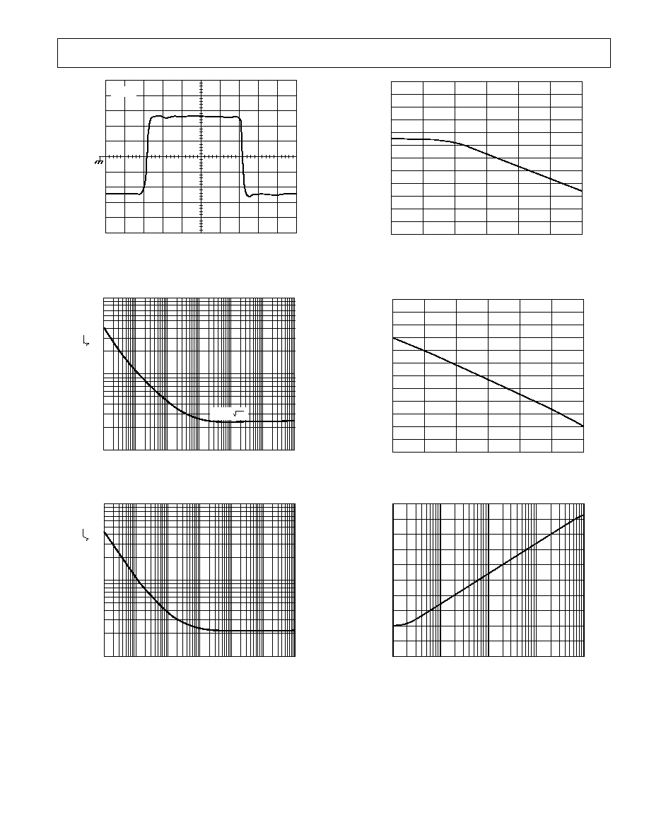
Driving Capacitive Loads
When the AD8021 drives a capacitive load, the high frequency
response may show excessive peaking before it rolls off. Two
techniques can be used to improve stability at high frequency
and reduce peaking. The first technique is to increase the compen-
sation capacitor, C
C
, which reduces the peaking while maintaining
gain flatness at low frequencies. The second technique is to add
a resistor, R
SNUB
, in series between the output pin of the AD8021
and the capacitive load, C
L
. Figure 15 shows the response of the
AD8021 when both C
C
and R
SNUB
are used to reduce peaking. For
a given C
L
, Figure 16 can be used to determine the value of R
SNUB
that maintains 2 dB of peaking in the frequency response. Please
note, however, that using R
SNUB
attenuates the low-frequency
output by a factor of R
LOAD
/(R
SNUB
+ R
LOAD
).
C
C
= 7pF;
R
SNUB
= 0
C
C
= 8pF;
R
SNUB
= 0
0.1
1000
1
10
100
FREQUENCY MHz
GAIN
dB
18
16
14
12
10
8
6
4
2
0
C
C
= 8pF;
R
SNUB
= 17.4
499
499
R
L
1k
49.9
49.9
C
C
33pF
FET
PROBE
V
S
R
SNUB
+V
S
5
6
Figure 15. Peaking vs. R
SNUB
and C
C
for C
L
= 33 pF
CAPACITIVE LOAD pF
0
50
R
SNUB
20
18
16
14
12
10
8
6
4
2
0
5
10
15
20
25
30
35
40
45
Figure 16. Relationship of R
SNUB
vs. C
L
for 2 dB Peaking at
a Gain of +2
REV. 0
AD8021
20
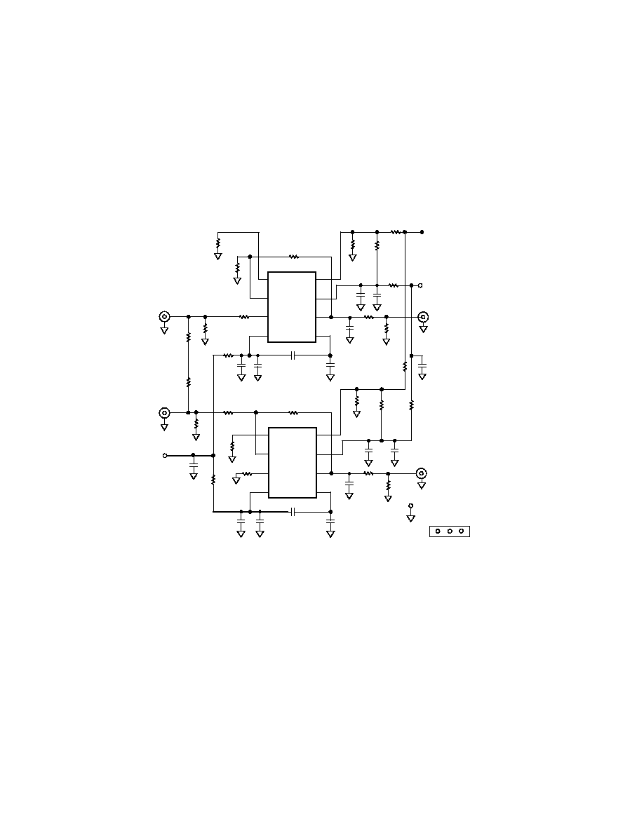
TP1
V
S
+V
S
GND
P1
R1
NON-INV. AMPLIFIER
LOGIC
REF
IN
+IN
V
S
V
OUT
C
COMP
+V
S
DIS
AD8021
1
2
3
4
8
7
6
5
+V
IN
R8
0
R7
R1
R23
0
R6
49.9
R25
0
C2
1nF
C1
0.1 F
C6
R22
0
V
IN
R20
49.9
R16
INV. AMPLIFIER
R4
C15
10 F
+
R21
0
C13
C10
F
C9
F
1
2
3
4
8
7
6
5
C11
R8
0
R11
R3
R2
R26
0
DISABLE
R10
0
R9
0
C4
0.1 F
C3
1nF
R4
0
C8
+V
S
+OUT
R18
0
R14
0
R15
0
R19
0
C14
C7
R1
OUT
R12
R13
C16
10 F
+
V
S
C12
0.1
1n
0.1 F
1nF
C5
SMA
SMA
LOGIC
REF
IN
+IN
V
S
V
OUT
C
COMP
+V
S
DIS
AD8021
Figure 17. Schematic of AD8021 Evaluation Board
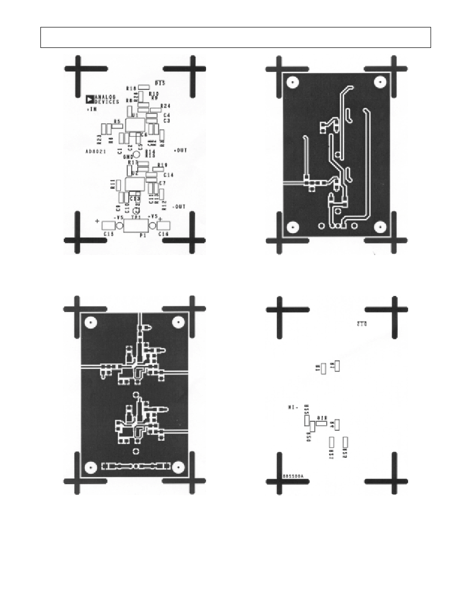
EVALUATION BOARD
A SOIC evaluation board is available for the AD8021. The board
provides both an inverting and noninverting circuit topology.
Evaluation Board Applications
Referring to the schematic of Figure 17, separate SMA input
connectors and termination resistors are provided for noninvert-
ing and inverting amplifiers. Separate amplifiers may be used as
a differential amplifier as in Figure 10.
In the differential configuration, either of the input SMA con-
nectors may be used and the amplifier inputs connected with
R22 and R23.
Resistors R9, R10, R14, and R15 may be omitted if the default
disable mode is used. Either amplifier may be disabled from an
external source. Zero
resistors R4, R19, R21, and R23 may
be removed to disable one of the amplifiers.
For gains of less than 10, refer to Figure 4 and Table I for the
value of the compensation capacitors C6 and C13.
REV. 0
AD8021
21
Figure 18. Evaluation Board Silkscreen (Top)
Figure 19. Evaluation Board Layout (Top)
Figure 20. Evaluation Board Layout (Bottom)
Figure 21. Evaluation Board Silkscreen (Bottom)
REV. 0
22
AD8021
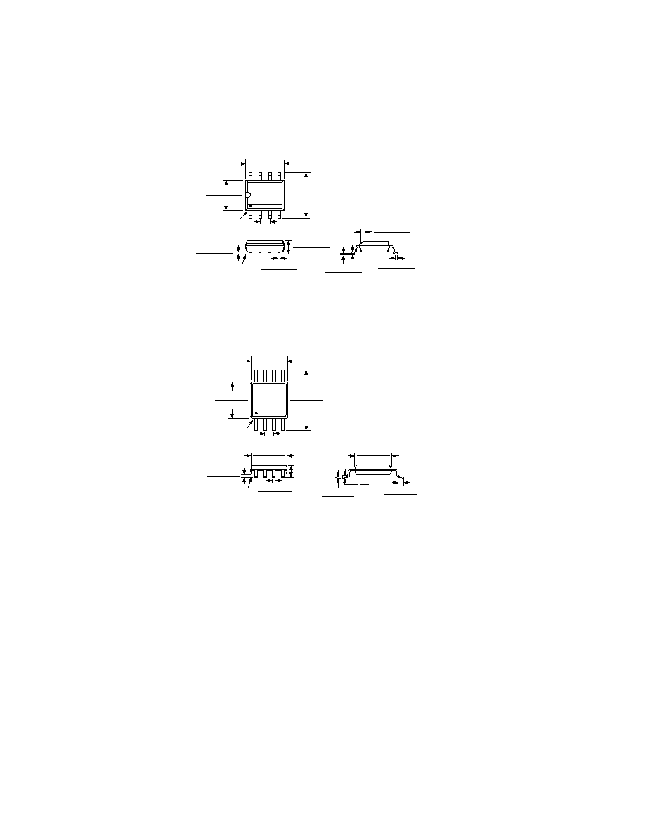
AD8021
8-Lead SOIC
(R-8)
0.0098 (0.25)
0.0075 (0.19)
0.0500 (1.27)
0.0160 (0.41)
8
0
0.0196 (0.50)
0.0099 (0.25)
45
8
5
4
1
0.1968 (5.00)
0.1890 (4.80)
0.2440 (6.20)
0.2284 (5.80)
PIN 1
0.1574 (4.00)
0.1497 (3.80)
0.0500 (1.27)
BSC
0.0688 (1.75)
0.0532 (1.35)
SEATING
PLANE
0.0098 (0.25)
0.0040 (0.10)
0.0192 (0.49)
0.0138 (0.35)
8-Lead MICRO_SOIC
(RM-8)
0.011 (0.28)
0.003 (0.08)
0.028 (0.71)
0.016 (0.41)
33
27
0.120 (3.05)
0.112 (2.84)
8
5
4
1
0.122 (3.10)
0.114 (2.90)
0.199 (5.05)
0.187 (4.75)
PIN 1
0.0256 (0.65) BSC
0.122 (3.10)
0.114 (2.90)
SEATING
PLANE
0.006 (0.15)
0.002 (0.05)
0.018 (0.46)
0.008 (0.20)
0.043 (1.09)
0.037 (0.94)
0.120 (3.05)
0.112 (2.84)
OUTLINE DIMENSIONS
Dimensions shown in inches and (mm).

23

24
C018881.57/01(0)
PRINTED IN U.S.A.