Äîêóìåíòàöèÿ è îïèñàíèÿ www.docs.chipfind.ru
8-Channel, 10- and 12-Bit ADCs with I
2
C-
Compatible Interface in 20-Lead TSSOP
AD7997/AD7998
Rev. 0
Information furnished by Analog Devices is believed to be accurate and reliable.
However, no responsibility is assumed by Analog Devices for its use, nor for any
infringements of patents or other rights of third parties that may result from its use.
Specifications subject to change without notice. No license is granted by implication
or otherwise under any patent or patent rights of Analog Devices. Trademarks and
registered trademarks are the property of their respective owners.
One Technology Way, P.O. Box 9106, Norwood, MA 02062-9106, U.S.A.
Tel: 781.329.4700
www.analog.com
Fax: 781.326.8703
© 2004 Analog Devices, Inc. All rights reserved.
FEATURES
10- and 12-bit ADC with fast conversion time: 2 µs typ
8 single-ended analog input channels
Specified for V
DD
of 2.7 V to 5.5 V
Low power consumption
Fast throughput rate: up to 188 kSPS
Sequencer operation
Automatic cycle mode
I
2
C®-compatible serial interface supports standard, fast,
and high speed modes
Out-of-range indicator/alert function
Pin-selectable addressing via AS
Shutdown mode: 1 µA max
Temperature range: -40°C to +85°C
20-lead TSSOP package
See the
AD7992
and
AD7994
for 2-channel and 4-channel
equivalent devices, respectively
GENERAL DESCRIPTION
The AD7997/AD7998 are 8-channel, 10- and 12-bit, low power,
successive approximation ADCs with an I
2
C-compatible
interface. The parts operate from a single 2.7 V to 5.5 V power
supply and feature a 2 µs conversion time. The parts contain an
8-channel multiplexer and track-and-hold amplifier that can
handle input frequencies up to 11 MHz.
The AD7997/AD7998 provide a 2-wire serial interface that is
compatible with I
2
C interfaces. Each part comes in two versions,
AD7997-0/AD7998-0 and AD7997-1/AD7998-1, and each
version allows at least two different I
2
C addresses. The I
2
C
interface on the AD7997-0/AD7998-0 supports standard and
fast I
2
C interface modes. The I
2
C interface on the AD7997-1/
AD7998-1 supports standard, fast, and high speed I
2
C interface
modes.
The AD7997/AD7998 normally remain in a shutdown state
while not converting, and power up only for conversions. The
conversion process can be controlled using the CONVST pin,
by a command mode where conversions occur across I
2
C write
operations or an automatic conversion interval mode selected
through software control.
The AD7997/AD7998 require an external reference that should
be applied to the REF
IN
pin and can be in the range of 1.2 V to
V
DD
. This allows the widest dynamic input range to the ADC.
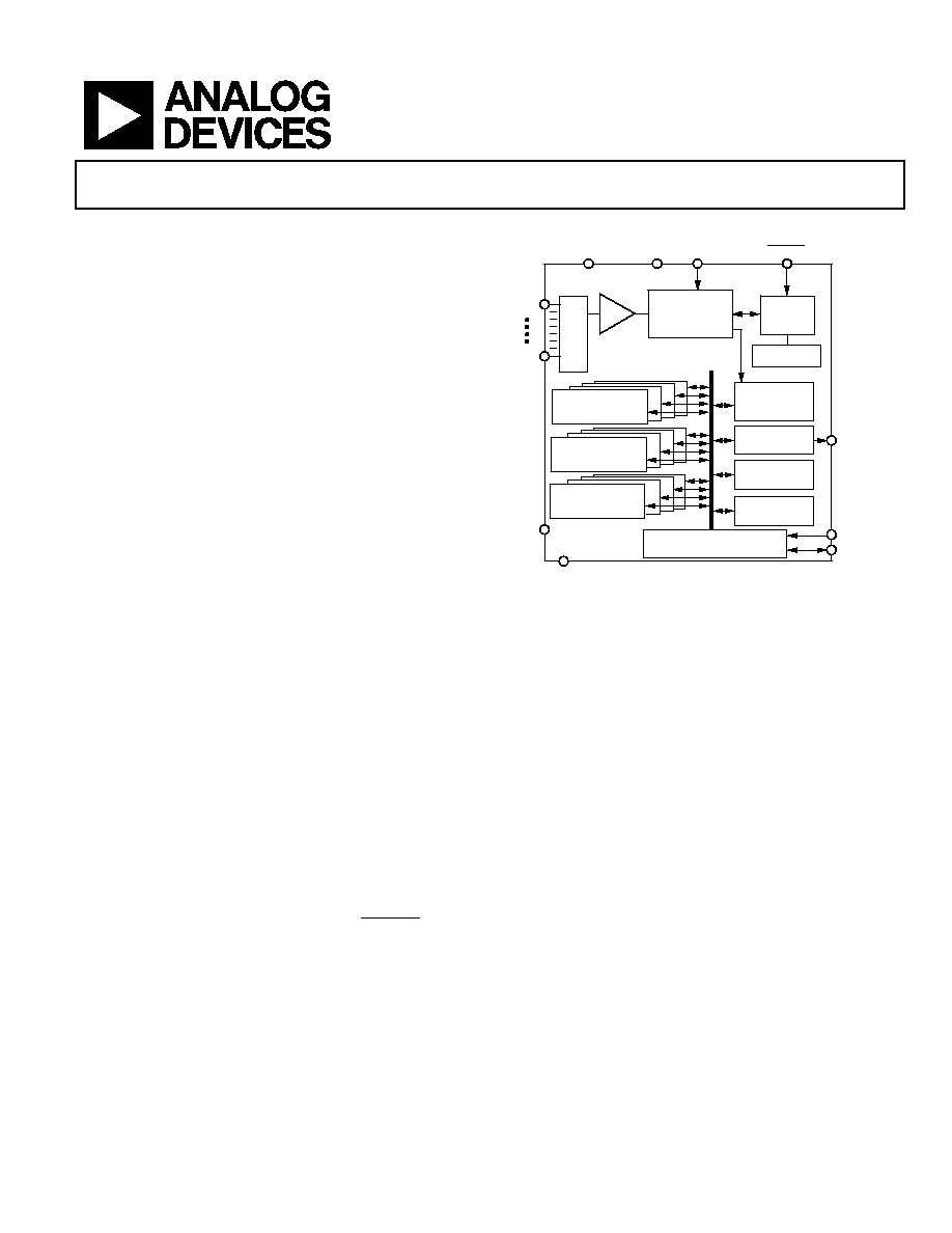
FUNCTIONAL BLOCK DIAGRAM
V
IN
1
10-/12-BIT
SUCCESSIVE
APPROXIMATION
ADC
CONTROL
LOGIC
8:1
I/P
MUX
AD7997/AD7998
V
DD
SCL
I
2
C INTERFACE
CYCLE TIMER
REGISTER
ALERT STATUS
REGISTER
CONFIGURATION
REGISTER
CONVERSION
RESULT
REGISTER
SDA
AGND
ALERT/BUSY
CONVST
AGND
AS
OSCILLATOR
REF
IN
V
IN
8
DATA
LOW
LIMIT
REGISTER CH1CH4
T/H
DATA
HIGH
LIMIT
REGISTER CH1CH4
HYSTERESIS
REGISTER CH1CH4
03473-
0-
001
Figure 1.
On-chip limit registers can be programmed with high and
low limits for the conversion result, and an open-drain, out-of-
range indicator output (ALERT) becomes active when the
programmed high or low limits are violated by the conversion
result. This output can be used as an interrupt.
PRODUCT HIGHLIGHTS
1.
2 µs conversion time with low power consumption.
2.
I
2
C-compatible serial interface with pin-selectable
addresses. Two AD7997/AD7998 versions allow five
AD7997/AD7998 devices to be connected to the same
serial bus.
3.
The parts feature automatic shutdown while not converting
to maximize power efficiency. Current consumption is 1 µA
max when in shutdown mode at 3V.
4.
Reference can be driven up to the power supply.
5.
Out-of-range indicator that can be software disabled or
enabled.
6.
One-shot and automatic conversion rates.
7.
Registers store minimum and maximum conversion
results.

AD7997/AD7998
Rev. 0 | Page 2 of 32
TABLE OF CONTENTS
AD7997 Specifications..................................................................... 3
AD7998 Specifications..................................................................... 5
I
2
C Timing Specifications ................................................................ 7
Absolute Maximum Ratings............................................................ 9
ESD Caution.................................................................................. 9
Pin Configuration and Pin Function Descriptions.................... 10
Terminology .................................................................................... 11
Typical Performance Characteristics ........................................... 12
Circuit Information ........................................................................ 15
Converter Operation.................................................................. 15
Typical Connection Diagram ................................................... 16
Analog Input ............................................................................... 16
Internal Register Structure ............................................................ 18
Address Pointer Register ........................................................... 18
Configuration Register .............................................................. 19
Conversion Result Register ....................................................... 20
Limit Registers ............................................................................ 20
Alert Status Register (CH1 to CH4) ........................................ 21
Cycle Timer Register.................................................................. 22
Sample Delay and Bit Trial Delay............................................. 22
Serial Interface ................................................................................ 23
Serial Bus Address ...................................................................... 23
Writing to the AD7997/AD7998 .................................................. 24
Writing to the Address Pointer Register for a Subsequent
Read.............................................................................................. 24
Writing a Single Byte of Data to the Alert Status Register or
Cycle Register.............................................................................. 24
Writing Two Bytes of Data to a Limit, Hysteresis, or
Configuration Register .............................................................. 24
Reading Data from the AD7997/AD7998................................... 26
ALERT/BUSY Pin .......................................................................... 27
SMBus ALERT ............................................................................ 27
BUSY ............................................................................................ 27
Placing the AD7997-1/AD7998-1 into High Speed Mode ... 27
The Address Select (AS) Pin ..................................................... 27
Modes of Operation ....................................................................... 28
Mode 1--Using the CONVST Pin ........................................... 28
Mode 2 COMMAND MODE ............................................... 29
Mode 3--Automatic Cycle Interval Mode.............................. 30
Outline Dimensions ....................................................................... 31
Ordering Guide .......................................................................... 31
Related Parts in I
2
C-Compatible ADC Product Family........ 31
REVISION HISTORY
9/04--Revision 0: Initial Version
AD7997/AD7998
Rev. 0 | Page 3 of 32
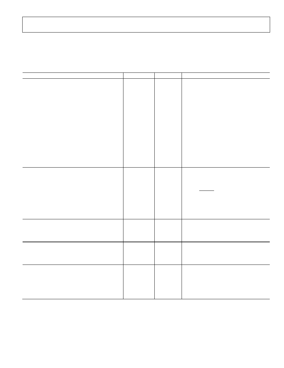
AD7997 SPECIFICATIONS
Temperature range for B version is -40°C to +85°C. Unless otherwise noted, V
DD
= 2.7 V to 5.5 V; REF
IN
= 2.5 V; For the AD7997-0, all
specifications apply for f
SCL
up to 400 kHz; for the AD7997-1, all specifications apply for f
SCL
up to 3.4 MHz, unless otherwise noted;
T
A
= T
MIN
to T
MAX
.
Table 1.
Parameter
B Version
Unit
Test Conditions/Comments
DYNAMIC PERFORMANCE
1
F
IN
= 10 kHz sine wave for f
SCL
from 1.7 MHz to
3.4 MHz
F
IN
= 1 kHz sine wave for f
SCL
up to 400 kHz
Signal to Noise + Distortion (SINAD)
2
61
dB min
Total Harmonic Distortion (THD)
2
75
dB max
Peak Harmonic or Spurious Noise (SFDR)
2
76
dB max
Intermodulation Distortion (IMD)
2
fa = 10.1 kHz, fb = 9.9 kHz for f
SCL
from 1.7 MHz
to 3.4 MHz
fa = 1.1 kHz, fb = 0.9 kHz for f
SCL
up to 400 kHz
Second-Order Terms
86
dB typ
Third-Order Terms
86
dB typ
Aperture Delay
2
10
ns max
Aperture Jitter
2
50
ps typ
Channel-to-Channel Isolation
2
90
dB typ
F
IN
= 108 Hz, see the Terminology section
Full-Power Bandwidth
2
11
MHz typ
@ 3 dB
2
MHz typ
@ 0.1 dB
DC ACCURACY
Resolution
10
Bits
Integral Nonlinearity
1, 2
±0.5
LSB max
Differential Nonlinearity
1, 2
±0.5
LSB max
Guaranteed no missed codes to 10 bits
Offset Error
2
±1.5
LSB max
Mode 1 (CONVST Mode)
±2.5
LSB max
Mode 2 (Command Mode)
Offset Error Match
2
±0.5
LSB max
Gain Error
2
±1.5 LSB
max
Gain Error Match
2
±0.5
LSB max
ANALOG INPUT
Input Voltage Range
0 to REF
IN
V
DC Leakage Current
±1
µA max
Input Capacitance
30
pF typ
REFERENCE INPUT
REF
IN
Input Voltage Range
1.2 to V
DD
V min/V max
DC Leakage Current
±1
µA max
Input Impedance
69
k typ
During a conversion
LOGIC INPUTS (SDA, SCL)
Input High Voltage, V
INH
0.7 (V
DD
)
V min
Input Low Voltage, V
INL
0.3 (V
DD
)
V max
Input Leakage Current, I
IN
±1
µA max
V
IN
= 0 V or V
DD
Input Capacitance, C
IN
3
10 pF
max
Input Hysteresis, V
HYST
0.1 (V
DD
)
V min

AD7997/AD7998
Rev. 0 | Page 4 of 32
Parameter
B Version
Unit
Test Conditions/Comments
LOGIC INPUTS (CONVST)
Input High Voltage, V
INH
2.4
V min
V
DD
= 5 V
2.0
V min
V
DD
= 3 V
Input Low Voltage, V
INL
0.8
V max
V
DD
= 5 V
0.4
V max
V
DD
= 3 V
Input Leakage Current, I
IN
±1
µA max
V
IN
= 0 V or V
DD
Input Capacitance, C
IN
3
10
pF max
LOGIC OUTPUTS (OPEN-DRAIN)
Output Low Voltage, V
OL
0.4
V max
I
SINK
= 3 mA
0.6
V max
I
SINK
= 6 mA
Floating-State Leakage Current
± 1
µA max
Floating-State Output Capacitance
3
10
pF max
Output Coding
Straight (Natural) Binary
CONVERSION RATE
See the Modes of Operation section
Conversion Time
2
µs typ
Throughput Rate
Mode 1 (Reading after the Conversion)
5
kSPS typ
f
SCL
= 100 kHz
21
kSPS
typ
f
SCL
= 400 kHz
121
kSPS
typ
f
SCL
= 3.4 MHz
Mode 2
5.5
kSPS typ
f
SCL
= 100 kHz
22
kSPS
typ
f
SCL
= 400 kHz
147
kSPS
typ
f
SCL
= 3.4 MHz, 188 kSPS typ @ 5 V
POWER REQUIREMENTS
V
DD
2.7/5.5
V min/max
I
DD
Digital inputs = 0 V or V
DD
Power-Down Mode, Interface Inactive
1/2
µA max
V
DD
= 3.3 V/5.5 V
Power-Down Mode, Interface Active
0.07/0.3
mA max
V
DD
= 3.3 V/5.5 V, 400 kHz f
SCL
0.3/0.6
mA max
V
DD
= 3.3 V/5.5 V, 3.4 MHz f
SCL
Operating, Interface Inactive
0.06/0.1
mA max
V
DD
= 3.3 V/5.5 V, 400 kHz f
SCL
0.3/0.6
mA max
V
DD
= 3.3 V/5.5 V, 3.4 MHz f
SCL
Operating, Interface Active
0.15/0.4
mA max
V
DD
= 3.3 V/5.5 V, 400 kHz f
SCL
0.6/1.1
mA max
V
DD
= 3.3 V/5.5 V, 3.4 MHz f
SCL
Mode 1
0.7/1.4
mA typ
V
DD
= 3.3 V/5.5 V, 3.4 MHz f
SCL
Mode 2
Mode 3 (I
2
C Inactive, T
CONVERT
x 32)
0.7/1.5
mA max
V
DD
= 3.3 V/5.5 V
Power Dissipation
Fully Operational
Operating, Interface Active
0.495/2.2
mW max
V
DD
= 3.3 V/5.5 V, 400 kHz f
SCL
1.98/6.05
mW
max
V
DD
= 3.3 V/5.5 V, 3.4 MHz f
SCL
Mode 1
2.31/7.7
mW
typ
V
DD
= 3.3 V/5.5 V, 3.4 MHz f
SCL
Mode 2
Power Down, Interface Inactive
3.3/11
µW max
V
DD
= 3.3 V/5.5 V
1
Max/min ac dynamic performance, INL and DNL specifications are typical specifications when operating in Mode 2 with I
2
C Hs-Mode SCL frequencies. Specifications
outlined for Mode 2 apply to Mode 3 also. Sample delay and bit trial delay enabled.
2
See the Terminology section.
3
Guaranteed by initial characterization.
AD7997/AD7998
Rev. 0 | Page 5 of 32
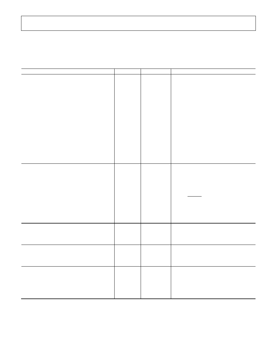
AD7998 SPECIFICATIONS
Temperature range for B version is -40°C to +85°C. Unless otherwise noted, V
DD
= 2.7 V to 5.5 V; REF
IN
= 2.5 V; For the AD7998-0, all
specifications apply for f
SCL
up to 400 kHz; for the AD7998-1, all specifications apply for f
SCL
up to 3.4 MHz, unless otherwise noted;
T
A
= T
MIN
to T
MAX
.
Table 2.
Parameter
B Version
Unit
Test Conditions/Comments
DYNAMIC PERFORMANCE
1
F
IN
= 10 kHz sine wave for f
SCL
from 1.7 MHz to
3.4 MHz
F
IN
= 1 kHz sine wave for f
SCL
up to 400 kHz
Signal-to-Noise + Distortion (SINAD)
2
70.5
dB min
Signal to Noise Ratio (SNR)
2
71 dB
min
Total Harmonic Distortion (THD)
2
78
dB max
Peak Harmonic or Spurious Noise (SFDR)
2
79
dB max
Intermodulation Distortion (IMD)
2
fa = 10.1 kHz, fb = 9.9 kHz f
SCL
from 1.7 MHz to
3.4 MHz
fa = 1.1 kHz, fb = 0.9 kHz for f
SCL
up to 400 kHz
Second-Order Terms
90
dB typ
Third-Order Terms
90
dB typ
Aperture Delay
2
10
ns max
Aperture Jitter
2
50
ps typ
Channel-to-Channel Isolation
2
90
dB typ
F
IN
= 108 Hz, see the Terminology section
Full-Power Bandwidth
2
11
MHz typ
@ 3 dB
2
MHz typ
@ 0.1 dB
DC ACCURACY
Resolution
12
Bits
Integral Nonlinearity
1,2
±1
LSB max
±0.2
LSB typ
Differential Nonlinearity
1,2
+1/0.9
LSB max
Guaranteed no missed codes to 12 bits
±0.2
LSB typ
Offset Error
2
±4
LSB max
Mode 1 (CONVST Mode)
±6
LSB max
Mode 2 (Command Mode)
Offset Error Match
2
±1
LSB max
Gain Error
2
±2
LSB max
Gain Error Match
2
±1
LSB max
ANALOG INPUT
Input Voltage Range
0 to REF
IN
V
DC Leakage Current
± 1
µA max
Input Capacitance
30
pF typ
REFERENCE INPUT
REF
IN
Input Voltage Range
1.2 to V
DD
V min/V max
DC Leakage Current
± 1
µA max
Input Impedance
69
k typ
LOGIC INPUTS (SDA, SCL)
Input High Voltage, V
INH
0.7 (V
DD
)
V min
Input Low Voltage, V
INL
0.3 (V
DD
)
V max
Input Leakage Current, I
IN
± 1
µA max
V
IN
= 0 V or V
DD
Input Capacitance, C
IN
3
10
pF max
Input Hysteresis, V
HYST
0.1 (V
DD
)
V min
AD7997/AD7998
Rev. 0 | Page 6 of 32
Parameter
B Version
Unit
Test Conditions/Comments
LOGIC INPUTS (CONVST)
Input High Voltage, V
INH
2.4
V min
V
DD
= 5 V
2.0
V min
V
DD
= 3 V
Input Low Voltage, V
INL
0.8
V max
V
DD
= 5 V
0.4
V max
V
DD
= 3 V
Input Leakage Current, I
IN
±1
µA max
V
IN
= 0 V or V
DD
Input Capacitance, C
IN
3
10
pF max
LOGIC OUTPUTS (OPEN-DRAIN)
Output Low Voltage, V
OL
0.4
V max
I
SINK
= 3 mA
0.6
V
max
I
SINK
= 6 mA
Floating-State Leakage Current
±1
µA max
Floating-State Output Capacitance
3
10
pF
max
Output Coding
Straight (Natural) Binary
CONVERSION RATE
See the Modes of Operation section
Conversion Time
2
µs typ
Throughput Rate
Mode 1 (Reading after the Conversion)
5
kSPS typ
f
SCL
= 100 kHz
21
kSPS
typ
f
SCL
= 400 kHz
121
kSPS
typ
f
SCL
= 3.4 MHz
Mode 2
5.5
kSPS typ
f
SCL
= 100 kHz
22
kSPS
typ
f
SCL
= 400 kHz
147
kSPS
typ
f
SCL
= 3.4 MHz , 188 kSPS typ @ 5 V
POWER REQUIREMENTS
V
DD
2.7/5.5 V
min/max
I
DD
Digital inputs = 0 V or V
DD
Power-Down Mode, Interface Inactive
1/2
µA max
V
DD
= 3.3 V/5.5 V
Power-Down Mode, Interface Active
0.07/0.3
mA max
V
DD
= 3.3 V/5.5 V, 400 kHz f
SCL
0.3/0.6
mA
max
V
DD
= 3.3 V/5.5 V, 3.4 MHz f
SCL
Operating, Interface Inactive
0.06/0.1
mA max
V
DD
= 3.3 V/5.5 V, 400 kHz f
SCL
0.3/0.6
mA
max
V
DD
= 3.3 V/5.5 V, 3.4 MHz f
SCL
Operating, Interface Active
0.15/0.4
mA max
V
DD
= 3.3 V/5.5 V, 400 kHz f
SCL
0.6/1.1
mA
max
V
DD
= 3.3 V/5.5 V, 3.4 MHz f
SCL
Mode 1
0.7/1.4
mA
typ
V
DD
= 3.3 V/5.5 V, 3.4 MHz f
SCL
Mode 2
Mode 3 (I
2
C Inactive, T
CONVERT
x 32)
0.7/1.5
mA max
V
DD
= 3.3 V/5.5 V
Power Dissipation
Fully Operational
Operating, Interface Active
0.495/2.2
mW max
V
DD
= 3.3 V/5.5 V, 400 kHz f
SCL
1.98/6.05
mW
max
V
DD
= 3.3 V/5.5 V, 3.4 MHz f
SCL
Mode 1
2.31/7.7
mW
typ
V
DD
= 3.3 V/5.5 V, 3.4 MHz f
SCL
Mode 2
Power Down, Interface Inactive
3.3/11
µW max
V
DD
= 3.3 V/5.5 V
1
Max/min ac dynamic performance, INL and DNL specifications are typical specifications when operating in Mode 2 with I
2
C Hs-Mode SCL frequencies. Specifications
outlined for Mode 2 apply to Mode 3 also. Sample delay and bit trial delay enabled.
2
See the
section.
Terminology
3
Guaranteed by initial characterization.
AD7997/AD7998
Rev. 0 | Page 7 of 32
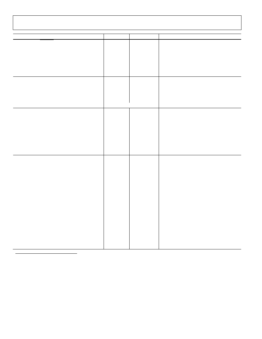
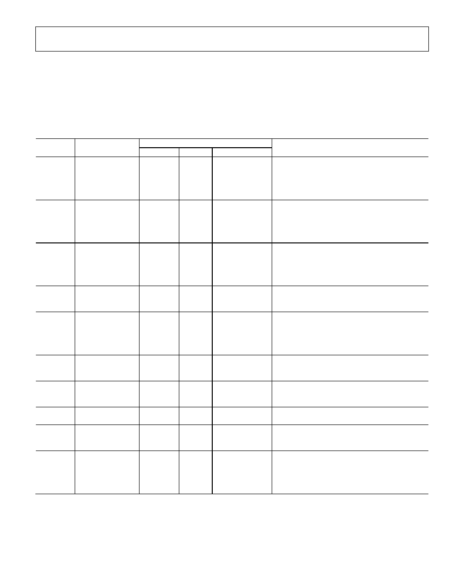
I
2
C TIMING SPECIFICATIONS
Guaranteed by initial characterization. All values measured with input filtering enabled. C
B
refers to capacitive load on the bus line. t
r
and
t
f
measured between 0.3 VDD and 0.7 VDD.
High speed mode timing specifications apply to the AD7997-1/AD7998-1 only. Standard and fast mode timing specifications apply to
both the AD7997-0/AD7998-0 and the AD7997-1/AD7998-1. See Figure 2. Unless otherwise noted, V
DD
= 2.7 V to 5.5 V; REF
IN
= 2.5 V;
T
A
=T
MIN
to T
MAX
.
Table 3.
AD7997/AD7998 Limit at T
MIN
, T
MAX
Parameter Conditions
Min
Max
Unit
Description
f
SCL
Standard mode
100
kHz
Serial clock frequency
Fast mode
400
kHz
High speed mode
C
B
= 100 pF max
3.4
MHz
C
B
= 400 pF max
1.7
MHz
t
1
Standard mode
4
µs
t
HIGH
, SCL high time
Fast mode
0.6
µs
High speed mode
C
B
= 100 pF max
60
ns
C
B
= 400 pF max
120
ns
t
2
Standard mode
4.7
µs
t
LOW
, SCL low time
Fast mode
1.3
µs
High speed mode
C
B
= 100 pF max
160
ns
C
B
= 400 pF max
320
ns
t
3
Standard mode
250
ns
t
SU;DAT
, data setup time
Fast mode
100
ns
High speed mode
10
ns
t
4
1
Standard mode
0
3.45
µs
t
HD;DAT
, data hold time
Fast mode
0
0.9
µs
High speed mode
C
B
= 100 pF max
0
70
2
ns
C
B
= 400 pF max
0
150
ns
t
5
Standard mode
4.7
µs
t
SU;STA
, setup time for a repeated start condition
Fast mode
0.6
µs
High speed mode
160
ns
t
6
Standard mode
4
µs
t
HD;STA
, hold time (repeated) start condition
Fast
mode 0.6
µs
High speed mode
160
ns
t
7
Standard mode
4.7
µs
t
BUF
, bus free time between a stop and a start condition
Fast
mode 1.3
µs
t
8
Standard mode
4
µs
t
SU;STO
, setup time for stop condition
Fast mode
0.6
µs
High speed mode
160
ns
t
9
Standard mode
1000
ns
t
RDA
, rise time of SDA signal
Fast mode
20 + 0.1 C
B
300
ns
High speed mode
C
B
= 100 pF max
10
80
ns
C
B
= 400 pF max
20
160
ns
AD7997/AD7998
Rev. 0 | Page 8 of 32
AD7997/AD7998 Limit at T
MIN
, T
MAX
Parameter Conditions
Min
Max
Unit
Description
t
10
Standard mode
300
ns
t
FDA
, fall time of SDA signal
Fast mode
20 + 0.1 C
B
300
ns
High speed mode
C
B
= 100 pF max
10
80
ns
C
B
= 400 pF max
20
160
ns
t
11
Standard mode
1000
ns
t
RCL
, rise time of SCL signal
Fast mode
20 + 0.1 C
B
300
ns
High speed mode
C
B
= 100 pF max
10
40
ns
C
B
= 400 pF max
20
80
ns
t
11A
Standard mode
1000
ns
t
RCL1
, rise time of SCL signal after a repeated start
condition and after an Acknowledge bit
Fast mode
20 + 0.1 C
B
300
ns
High speed mode
C
B
= 100 pF max
10
80
ns
C
B
= 400 pF max
20
160
ns
t
12
Standard mode
300
ns
t
FCL
, fall time of SCL signal
Fast mode
20 + 0.1 C
B
300
ns
High speed mode
C
B
= 100 pF max
10
40
ns
C
B
= 400 pF max
20
80
ns
t
SP
Fast mode
0
50
ns
Pulse width of suppressed spike
High speed mode
0
10
ns
t
POWER-UP
1
typ µs
Power-up time
1
A device must provide a data hold time for SDA in order to bridge the undefined region of the SCL falling edge.
2
For 3 V supplies, the maximum hold time with
C
B
= 100 pF max is 100 ns max.
P
S
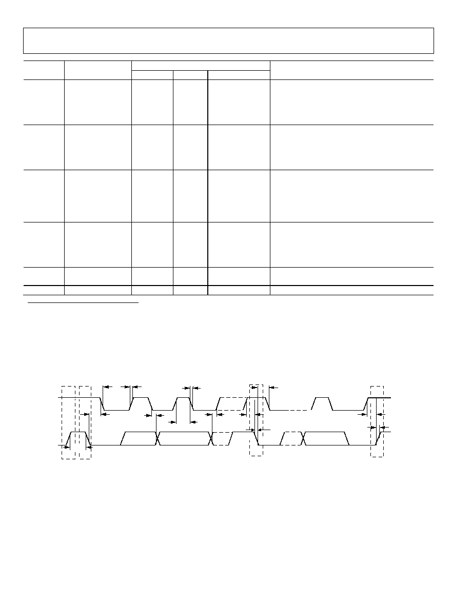
S
P
t
6
t
4
t
1
t
3
t
5
t
8
t
2
t
11
t
12
t
6
SCL
SDA
t
7
t
9
t
10
S = START CONDITION
P = STOP CONDITION
03473-0-002
Figure 2. Timing Diagram for 2-Wire Serial Interface
AD7997/AD7998
Rev. 0 | Page 9 of 32
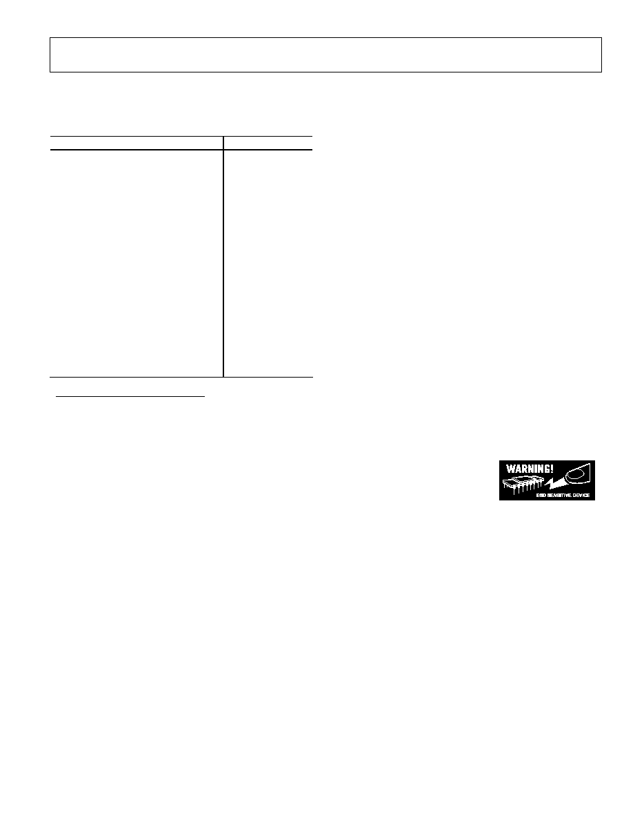
ABSOLUTE MAXIMUM RATINGS
T
A
= 25°C, unless otherwise noted.
Table 4.
Parameter Rating
V
DD
to GND
-0.3 V to 7 V
Analog Input Voltage to GND
-0.3 V to V
DD
+ 0.3 V
Reference Input Voltage to GND
-0.3 V to V
DD
+ 0.3 V
Digital Input Voltage to GND
-0.3 V to +7 V
Digital Output Voltage to GND
-0.3 V to V
DD
+ 0.3 V
Input Current to Any Pin Except Supplies
1
±10 mA
Operating Temperature Range
Commercial (B Version)
-40°C to +85°C
Storage Temperature Range
-65°C to +150°
Junction Temperature
150°C
20-Lead TSSOP
JA
Thermal Impedance
143°C/W
JC
Thermal Impedance
45°C/W
Pb/SN Temperature, Soldering
Reflow (10 s to 30 s)
240 (+0/-5)°C
Pb-free Temperature, Soldering
Reflow 260
(+0)°C
ESD 1.5
kV
1
Transient currents of up to 100 mA do not cause SCR latch-up.
Stresses above those listed under Absolute Maximum Ratings
may cause permanent damage to the device. This is a stress
rating only; functional operation of the device at these or any
other conditions above those listed in the operational sections
of this specification is not implied. Exposure to absolute
maximum rating conditions for extended periods may affect
device reliability.
ESD CAUTION
ESD (electrostatic discharge) sensitive device. Electrostatic charges as high as 4000 V readily accumulate on
the human body and test equipment and can discharge without detection. Although this product features
proprietary ESD protection circuitry, permanent damage may occur on devices subjected to high energy
electrostatic discharges. Therefore, proper ESD precautions are recommended to avoid performance
degradation or loss of functionality.
AD7997/AD7998
Rev. 0 | Page 10 of 32
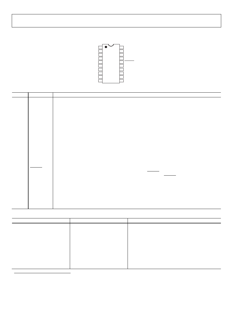
PIN CONFIGURATION AND PIN FUNCTION DESCRIPTIONS
AD7997/
AD7998
TOP VIEW
1
2
3
4
17
18
19
20
SDA
SCL
V
DD
AGND
V
IN
4
14
13
V
IN
2
5
(Not to Scale)
ALERT/BUSY
16
V
DD
15
AS
AGND
REF
IN
6
V
IN
1
7
V
IN
3
8
AGND
AGND
V
IN
5
9
V
IN
7
10
V
IN
8
12
11
V
IN
6
03473-0-003
CONVST
Figure 3. AD7998/AD7997 Pin Configuration
Table 5. Pin Function Descriptions
Pin No.
Mnemonic
Function
1, 3,
4, 20
AGND
Analog Ground. Ground reference point for all circuitry on the AD7997/AD7998. All analog input signals should be
referred to this AGND voltage.
2, 5
V
DD
Power Supply Input. The V
DD
range for the AD7997/AD7998 is from 2.7 V to 5.5 V.
6 REF
IN
Voltage Reference Input. The external reference for the AD7997/AD7998 should be applied to this input pin. The
voltage range for the external reference is 1.2 V to V
DD
. A 0.1 µF and 1 µF capacitors should be placed between REF
IN
and AGND. See Typical Connection Diagram.
7 V
IN
1
Analog Input 1. Single-ended analog input channel. The input range is 0 V to REF
IN
.
8 V
IN
3
Analog Input 3. Single-ended analog input channel. The input range is 0 V to REF
IN
.
9 V
IN
5
Analog Input 5. Single-ended analog input channel. The input range is 0 V to REF
IN
.
10 V
IN
7
Analog Input 7. Single-ended analog input channel. The input range is 0 V to REF
IN
.
11 V
IN
8
Analog Input 8. Single-ended analog input channel. The input range is 0 V to REF
IN
.
12 V
IN
6
Analog Input 6. Single-ended analog input channel. The input range is 0 V to REF
IN
.
13 V
IN
4
Analog Input 4. Single-ended analog input channel. The input range is 0 V to REF
IN
.
14 V
IN
2
Analog Input 2. Single-ended analog input channel. The input range is 0 V to REF
IN
.
15 AS
Logic Input. Address select input that selects one of three I
2
C addresses for the AD7997/AD7998, as shown in Table
6
.
The device address depends on the voltage applied to this pin.
16
CONVST
Logic Input Signal. Convert start signal. This is an edge-triggered logic input. The rising edge of this signal powers up
the part. The power-up time for the part is 1 µs. The falling edge of CONVST places the track/hold into hold mode and
initiates a conversion. A power-up time of at least 1 µs must be allowed for the CONVST high pulse; otherwise, the
conversion result is invalid (see the Modes of Operation section).
17
ALERT/BUSY
Digital Output. Selectable as an ALERT or BUSY output function. When configured as an ALERT, this pin acts as an out-
of-range indicator and, if enabled, becomes active when the conversion result violates the DATAHIGH or DATALOW
register values. See the Limit Registers section. When configured as a BUSY output, this pin becomes active when a
conversion is in progress. Open-drain output.
18
SDA
Digital I/O. Serial bus bidirectional data. Open-drain output. External pull-up resistor required.
19
SCL
Digital Input. Serial bus clock. Open-drain input. External pull-up resistor required.
Table 6. I
2
C Address Selection
Part Number
AS Pin
I
2
C Address
AD7997-0
AGND
010 0001
AD7997-0
V
DD
010 0010
AD7997-1
AGND
010 0011
AD7997-1
V
DD
010 0100
AD7997-x
1
Float
010 0000
AD7998-0
AGND
010 0001
AD7998-0
V
DD
010 0010
AD7998-1
AGND
010 0011
AD7998-1
V
DD
010 0100
AD7998-x
1
Float 010
0000
1
If the AS pin is left floating on any of the AD7997/AD7998 parts, the device address is 010 0000.

AD7997/AD7998
Rev. 0 | Page 11 of 32
TERMINOLOGY
Signal-to-Noise and Distortion Ratio (SINAD)
The measured ratio of signal-to-noise and distortion at the out-
put of the A/D converter. The signal is the rms amplitude of the
fundamental. Noise is the sum of all nonfundamental signals up
to half the sampling frequency (f
S
/2), excluding dc. The ratio is
dependent on the number of quantization levels in the digiti-
zation process; the more levels, the smaller the quantization
noise. The theoretical signal-to-noise and distortion ratio for
an ideal N-bit converter with a sine wave input is given by
Signal-to-(Noise + Distortion) = (6.02 N + 1.76) dB
Thus, the SINAD is 61.96 dB for a 10-bit converter and 74 dB
for a 12-bit converter.
Total Harmonic Distortion (THD)
The ratio of the rms sum of harmonics to the fundamental. For
the AD7997/AD7998, it is defined as
1
6
5
4
3
2
V
V
V
V
V
V
THD
2
2
2
2
2
log
20
)
dB
(
+
+
+
+
=
where V
1
is the rms amplitude of the fundamental and V
2
, V
3
,
V
4
, V
5
, and V
6
are the rms amplitudes of the second through
sixth harmonics.
Peak Harmonic or Spurious Noise
The ratio of the rms value of the next largest component in the
ADC output spectrum (up to f
S
/2 and excluding dc) to the rms
value of the fundamental. Typically, the value of this specification
is determined by the largest harmonic in the spectrum, but for
ADCs where the harmonics are buried in the noise floor, it is a
noise peak.
Intermodulation Distortion
With inputs consisting of sine waves at two frequencies, fa
and fb, any active device with nonlinearities creates distortion
products at sum and difference frequencies of mfa ± nfb, where
m, n = 0, 1, 2, 3, and so on. Intermodulation distortion terms
are those for which neither m nor n equal zero. For example,
second-order terms include (fa + fb) and (fa - fb), while
third-order terms include (2fa + fb), (2fa - fb),(fa + 2fb) and
(fa - 2fb).
The AD7997/AD7998 is tested using the CCIF standard where
two input frequencies near the top end of the input bandwidth
are used. In this case, the second-order terms are usually dis-
tanced in frequency from the original sine waves while the
third-order terms are usually at a frequency close to the input
frequencies. As a result, the second and third-order terms are
specified separately. The calculation of intermodulation distor-
tion is, like the THD specification, the ratio of the rms sum of
the individual distortion products to the rms amplitude of the
sum of the fundamentals, expressed in dB.
Channel-to-Channel Isolation
A measure of the level of crosstalk between channels, taken
by applying a full-scale sine wave signal to the unselected input
channels, and determining how much the 108 Hz signal is
attenuated in the selected channel. The sine wave signal applied
to the unselected channels is then varied from 1 kHz up to
2 MHz, each time determining how much the 108 Hz signal in
the selected channel is attenuated. This figure represents the
worst-case level across all channels.
Aperture Delay
The measured interval between the sampling clock's leading
edge and the point at which the ADC takes the sample.
Aperture Jitter
This is the sample-to-sample variation in the effective point in
time at which the sample is taken.
Full-Power Bandwidth
The input frequency at which the amplitude of the reconstructed
fundamental is reduced by 0.1 dB or 3 dB for a full-scale input.
Power Supply Rejection Ratio (PSRR)
The ratio of the power in the ADC output at the full-scale
frequency, f, to the power of a 200 mV p-p sine wave applied
to the ADC V
DD
supply of frequency f
S
:
PSRR (dB) = 10 log (Pf/Pf
S
)
where Pf is the power at frequency f in the ADC output; Pf
S
is
the power at frequency f
S
coupled onto the ADC V
DD
supply.
Integral Nonlinearity
The maximum deviation from a straight line passing through
the endpoints of the ADC transfer function. The endpoints are
zero scale, a point 1 LSB below the first code transition, and full
scale, a point 1 LSB above the last code transition.
Differential Nonlinearity
The difference between the measured and the ideal 1 LSB
change between any two adjacent codes in the ADC.
Offset Error
The deviation of the first code transition (00...000) to
(00...001) from the ideal--that is, AGND + 1 LSB.
Offset Error Match
The difference in offset error between any two channels.
Gain Error
The deviation of the last code transition (111...110) to
(111...111) from the ideal (that is, REF
IN
- 1 LSB) after the
offset error has been adjusted out.
Gain Error Match
The difference in gain error between any two channels.
AD7997/AD7998
Rev. 0 | Page 12 of 32
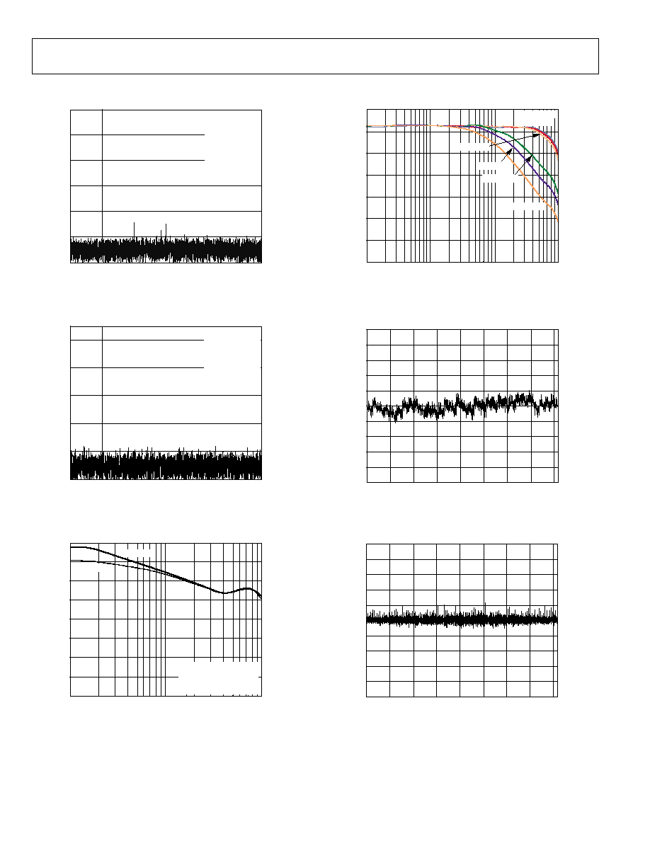
TYPICAL PERFORMANCE CHARACTERISTICS
120
100
80
60
40
20
0
S
I
NAD (dB)
20
40
0
60
FREQUENCY (kHz)
03473-0-004
FS = 121kSPS
FSCL = 3.4MHz
FIN = 10kHz
SNR = 71.84dB
SINAD = 71.68dB
THD = 86.18dB
SFDR = 88.70dB
Figure 4. AD7998 Dynamic Performance with 5 V Supply and
2.5 V Reference, 121 kSPS, Mode 1
110
90
70
50
30
10
S
I
NAD (dB)
10
40
0
60
40
45
50
60
70
75
S
I
NAD (dB)
1
1000
FREQUENCY (kHz)
03473-0-007
100
10
V
DD
= 4.5V
V
DD
= 3V
V
DD
= 2.7V
V
DD
= 3.3V
V
DD
= 5V
65
55
V
DD
= 5.5V
INPUT FREQUENCY (kHz)
03473-0-005
20
30
50
FS = 121kSPS
FSCL = 3.4MHz
FIN = 10kHz
SINAD = 61.63dB
THD = 91.82dB
SFDR = 94.95dB
Figure 5. AD7997 Dynamic Performance with 5 V Supply and
2.5 V Reference, 121 kSPS, Mode 1
20
40
70
80
90
100
P
S
RR (dB)
10
1000
SUPPLY RIPPLE FREQUENCY (kHz)
03473-0-006
100
V
DD
= 3V
V
DD
= 5V
50
30
60
V
DD
= 3V/5V
200mV p-p SINE WAVE
ON V
DD
2nF CAPACITOR ON V
DD
Figure 6. PSRR vs. Supply Ripple Frequency
Figure 7. AD7998 SINAD vs. Analog Input Frequency for
Various Supply Voltages, 3.4 MHz f
SCL
, 136 kSPS
1.0
0.8
0.6
0.4
0.2
0
0.2
0.4
0.6
0.8
1.0
INL E
RROR (LS
B
)
2000
1500
500
1000
0
2500
3000
3500
4000
CODE
03473-0-008
Figure 8. Typical INL, V
DD
= 5.5 V, Mode 1, 3.4 MHz f
SCL
, 121 kSPS
1.0
0.8
0.6
0.4
0.2
0
0.2
0.4
0.6
0.8
1.0
DNL E
RROR (LS
B
)
2000
1500
500
1000
0
2500
3000
3500
4000
CODE
03473-0-009
Figure 9. Typical DNL, V
DD
= 5.5 V, Mode 1, 3.4 MHz f
SCL
, 121 kSPS
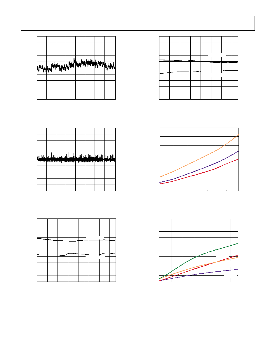
AD7997/AD7998
Rev. 0 | Page 13 of 32
1.0
0.8
0.6
0.4
0.2
0
0.2
0.4
0.6
0.8
1.0
INL E
RROR (LS
B
)
2000
1500
500
1000
0
2500
3000
3500
4000
CODE
03473-0-010
Figure 10. Typical INL, V
DD
= 2.7 V, Mode 1, 3.4 MHz f
SCL
, 121 kSPS
1.0
0.8
0.6
0.4
0.2
0
0.2
0.4
0.6
0.8
1.0
DNL E
RROR (LS
B
)
2000
1500
500
1000
0
2500
3000
3500
4000
CODE
03473-0-011
Figure 11. Typical DNL, V
DD
= 2.7 V, Mode 1, 3.4 MHz f
SCL
, 121 kSPS
INL E
RROR (LS
B
)
REFERENCE VOLTAGE (V)
03473-0-012
1.0
0.8
-0.6
0.4
0.2
0
0.2
0.4
0.6
0.8
1.0
1.2
1.7
2.2
2.7
3.2
3.7
4.2
4.7
POSITIVE INL
NEGATIVE INL
Figure 12. AD7998 Change in INL vs. Reference Voltage V
DD
= 5 V,
Mode 1, 121 kSPS
DNL E
RROR (LS
B
)
REFERENCE VOLTAGE (V)
03473-0-013
1.0
0.8
-0.6
0.4
0.2
0
0.2
0.4
0.6
0.8
1.0
1.2
1.7
2.2
2.7
3.2
3.7
4.2
4.7
POSITIVE DNL
NEGATIVE DNL
Figure 13. AD7998 Change in DNL vs. Reference Voltage V
DD
= 5 V,
Mode 1, 121 kSPS
S
U
P
P
L
Y
CURRE
NT (mA)
SUPPLY VOLTAGE (V)
03473-0-014
0
0.0001
0.0002
0.0003
0.0004
0.0005
0.0006
0.0007
2.7
3.2
3.7
4.2
4.7
5.2
+25
°
C
+85
°
C
40
°
C
Figure 14. AD7998 Shutdown Current vs. Supply Voltage,
40°C, +25°C, and +85°C
S
U
P
P
L
Y
CURRE
NT (mA)
SCL FREQUENCY (kHz)
03473-0-015
0
0.2
0.4
0.6
0.8
1.0
1.2
1.4
1.6
1.8
2.0
100
600
1100
1600
2100
2600
3100
MODE 1
VDD = 5V
MODE 1
VDD = 3V
MODE 2
VDD = 5V
MODE 2
VDD = 3V
Figure 15. AD7998 Average Supply Current vs. I
2
C Bus Rate for
V
DD
= 3 V and 5 V
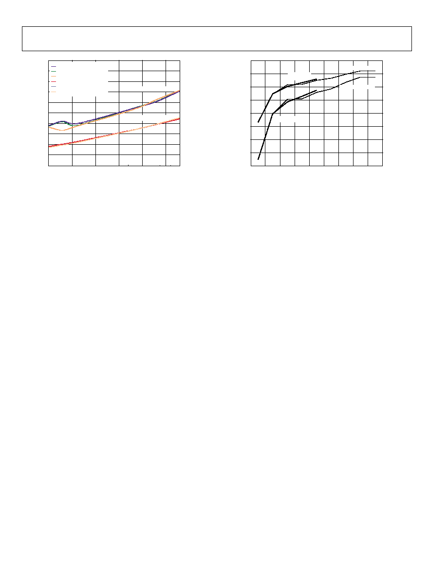
AD7997/AD7998
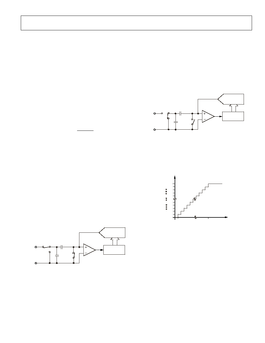
Rev. 0 | Page 14 of 32
S
U
P
P
L
Y
CURRE
NT (mA)
SUPPLY VOLTAGE (V)
03473-0-016
0
0.2
0.4
0.6
0.8
1.0
1.2
1.4
1.6
1.8
2.0
2.7
3.2
3.7
4.2
4.7
5.2
MODE 2 - 147kSPS
MODE 1 - 121kSPS
TEMPERATURE = +85
°
C
TEMPERATURE = +25
°
C
TEMPERATURE = 40
°
C
TEMPERATURE = +85
°
C
TEMPERATURE = +25
°
C
TEMPERATURE = 40
°
C
Figure 16. AD7998 Average Supply Current vs. Supply Voltage
for Various Temperatures
03473-0-017
10.4
10.6
10.8
11.0
11.2
11.4
11.6
11.8
12.0
1.200 2.048 2.500 2.700 3.000 3.300 4.096 4.500 5.000
REFERENCE VOLTAGE (V)
ENOB (
B
ITS)
68
69
70
71
72
73
74
S
I
NAD (dB)
ENOB V
DD
= 3V
ENOB V
DD
= 5V
SINAD V
DD
= 3V
SINAD V
DD
= 5V
Figure 17. SINAD/ENOB vs. Reference Voltage, Mode 1, 121 kSPS
AD7997/AD7998
Rev. 0 | Page 15 of 32
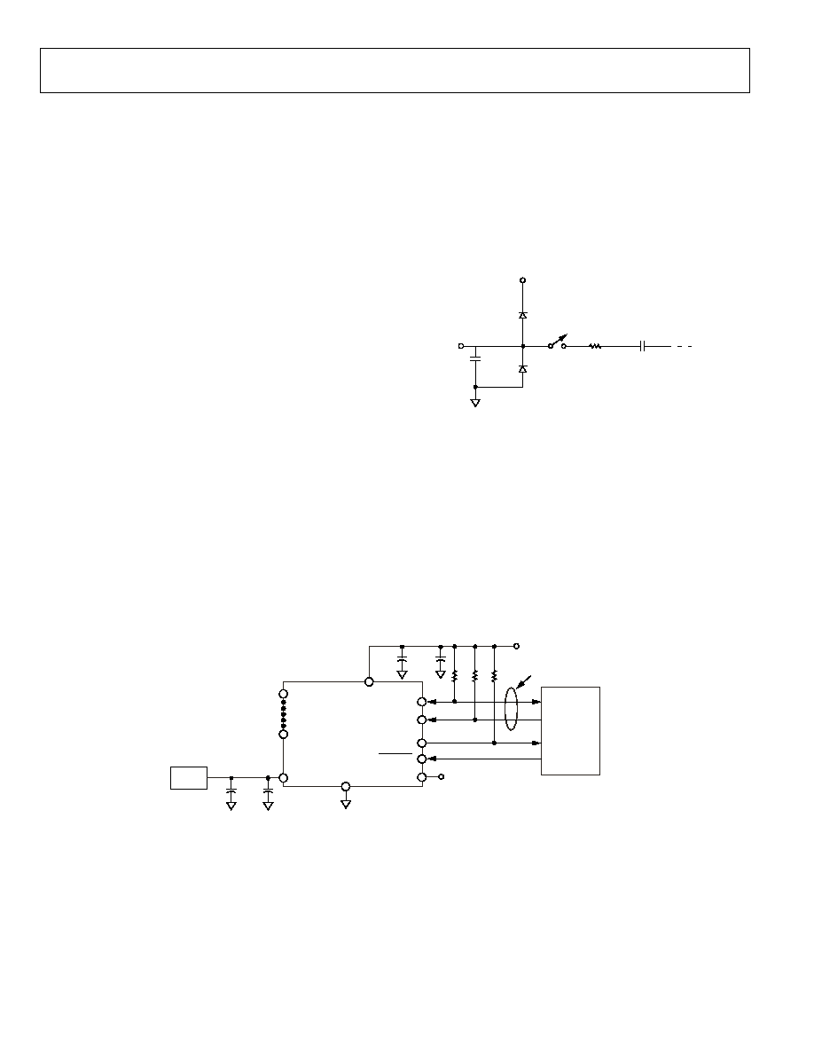
CIRCUIT INFORMATION
The AD7997/AD7998 are low power, 10- and 12-bit, single-
supply, 8-channel A/D converters. The parts can be operated
from a 2.7 V to 5.5 V supply.
The AD7997/AD7998 have an 8-channel multiplexer, an on-
chip track-and-hold, an A/D converter, an on-chip oscillator,
internal data registers, and an I
2
C-compatible serial interface, all
housed in a 20-lead TSSOP. This package offers considerable
space-saving advantages over alternative solutions. The
AD7997/AD7998 require an external reference in the range of
1.2 V to V
DD
.
The AD7997/AD7998 typically remain in a power-down state
while not converting. When supplies are first applied, the parts
come up in a power-down state. Power-up is initiated prior to
a conversion, and the device returns to shutdown when the
conversion is complete. Conversions can be initiated on the
AD7997/AD7998 by pulsing the CONVST signal, using an
automatic cycle interval mode, or a command mode where
wake-up and a conversion occur during a write address
function (see the Modes of Operation section). When the
conversion is complete, the AD7997/AD7998 again enter
shutdown mode. This automatic shutdown feature allows power
saving between conversions. This means any read or write
operation across the I
2
C interface can occur while the device is
in shutdown.
CONVERTER OPERATION
The AD7997/AD7998 are successive approximation analog-to-
digital converters based around a capacitive DAC. Figure 18
and Figure 19 show simplified schematics of the ADC during
the acquisition and conversion phase, respectively. Figure 18
shows the acquisition phase. SW2 is closed and SW1 is in
position A, the comparator is held in a balanced condition,
and the sampling capacitor acquires the signal on V
IN
.
CAPACITIVE
DAC
V
IN
COMPARATOR
CONTROL
LOGIC
SW1
A
B
SW2
AGND
03473-0-018
Figure 18. ADC Acquisition Phase
At the beginning of a conversion, SW2 opens and SW1 moves
to position B, causing the comparator to become unbalanced, as
shown in Figure 19. The input is disconnected once the con-
version begins. The control logic and the capacitive DAC are
used to add and subtract fixed amounts of charge from the
sampling capacitor to bring the comparator back into a
balanced condition. When the comparator is rebalanced, the
conversion is complete. The control logic generates the ADC
output code. Figure 20 shows the ADC transfer characteristic.
V
IN
COMPARATOR
CONTROL
LOGIC
SW1
A
B
SW2
AGND
CAPACITIVE
DAC
03473-0-019
Figure 19. ADC Conversion Phase
ADC Transfer Function
The output coding of the AD7997/AD7998 is straight binary.
The designed code transitions occur at successive integer LSB
values (1 LSB, 2 LSB, and so on). The LSB size is REF
IN
/1024 for
the AD7997 and REF
IN
/4096 for the AD7998. Figure 20 shows
the ideal transfer characteristic for the AD7997/AD7998.
000...000
ADC
CODE
ANALOG INPUT
0V TO REF
IN
111...111
000...001
000...010
111...110
111...000
011...111
AGND + 1LSB
+REF
IN
1LSB
AD7998 1LSB = REF
IN
/4096
03473-0-020
AD7997 1LSB = REF
IN
/1024
Figure 20. AD7997/AD7998 Transfer Characteristic
AD7997/AD7998
Rev. 0 | Page 16 of 32
TYPICAL CONNECTION DIAGRAM
The typical connection diagram for the AD7997/AD7998 is
shown in Figure 22. In this figure, the address select pin (AS)
is tied to V
DD
; however, AS can also be tied to AGND or left
floating, allowing the user to select up to five AD7997/AD7998
devices on the same serial bus. An external reference must be
applied to the AD7997/AD7998. This reference can be in the
range of 1.2 V to V
DD
. A precision reference like the REF 19x
family, AD780, ADR03, or ADR381 can be used to supply the
reference voltage to the ADC.
SDA and SCL form the 2-wire I
2
C-/SMBus-compatible
interface. External pull-up resisters are required for both SDA
and SCL lines.
The AD7998-0/AD7997-0 support standard and fast I
2
C
interface modes. The AD7998-1/AD7997-1 support standard,
fast, and high speed I
2
C interface modes. Therefore if operating
in either standard or fast mode, up to five AD7997/AD7998
devices can be connected to the bus, as noted:
3 × AD7997-0/AD7998-0 and 2 × AD7997-1/ AD7998-1
or
3 × AD7997-1/AD7998-1 and 2 × AD7997-0/AD7998-0
In high speed mode, up to three AD7997-1/AD7998-1 devices
can be connected to the bus.
Wake-up from shutdown and acquisition prior to a conversion
is approximately 1 µs, and conversion time is approximately
2 µs. The AD7997/AD7998 enters shutdown mode again after
each conversion, which is useful in applications where power
consumption is a concern.
ANALOG INPUT
Figure 21 shows an equivalent circuit of the AD7997/AD7998
analog input structure. The two diodes, D1 and D2, provide
ESD protection for the analog inputs. Care must be taken to
ensure that the analog input signal does not exceed the supply
rails by more than 300 mV. This causes the diodes to become
forward biased and start conducting current into the substrate.
These diodes can conduct a maximum current of 10 mA
without causing irreversible damage to the part.
V
IN
D1
V
DD
D2
R1
C2
30pF
C1
4pF
CONVERSION PHASE--SWITCH OPEN
TRACK PHASE--SWITCH CLOSED
03473-0-022
Figure 21. Equivalent Analog Input Circuit
Capacitor C1 in Figure 21 is typically about 4 pF and can
primarily be attributed to pin capacitance. Resistor R1 is a
lumped component made up of the on resistance (R
ON
) of
a track-and-hold switch, and also includes the R
ON
of the
input multiplexer. The total resistance is typically about 400 .
C2, the ADC sampling capacitor, has a typical capacitance of
30 pF.
V
DD
V
IN
1
AGND
5V SUPPLY
REF 19x
1
µ
F
0.1
µ
F
10
µ
F
AD7997/
AD7998
0V to REF
IN
INPUT
SDA
µ
C/
µ
P
SCL
2-WIRE SERIAL
INTERFACE
CONVST
ALERT
REF
IN
R
P
R
P
R
P
V
DD
AS
V
IN
8
03473-0-021
0.1
µ
F
Figure 22. AD7997/AD7998 Typical Connection Diagram
AD7997/AD7998
Rev. 0 | Page 17 of 32
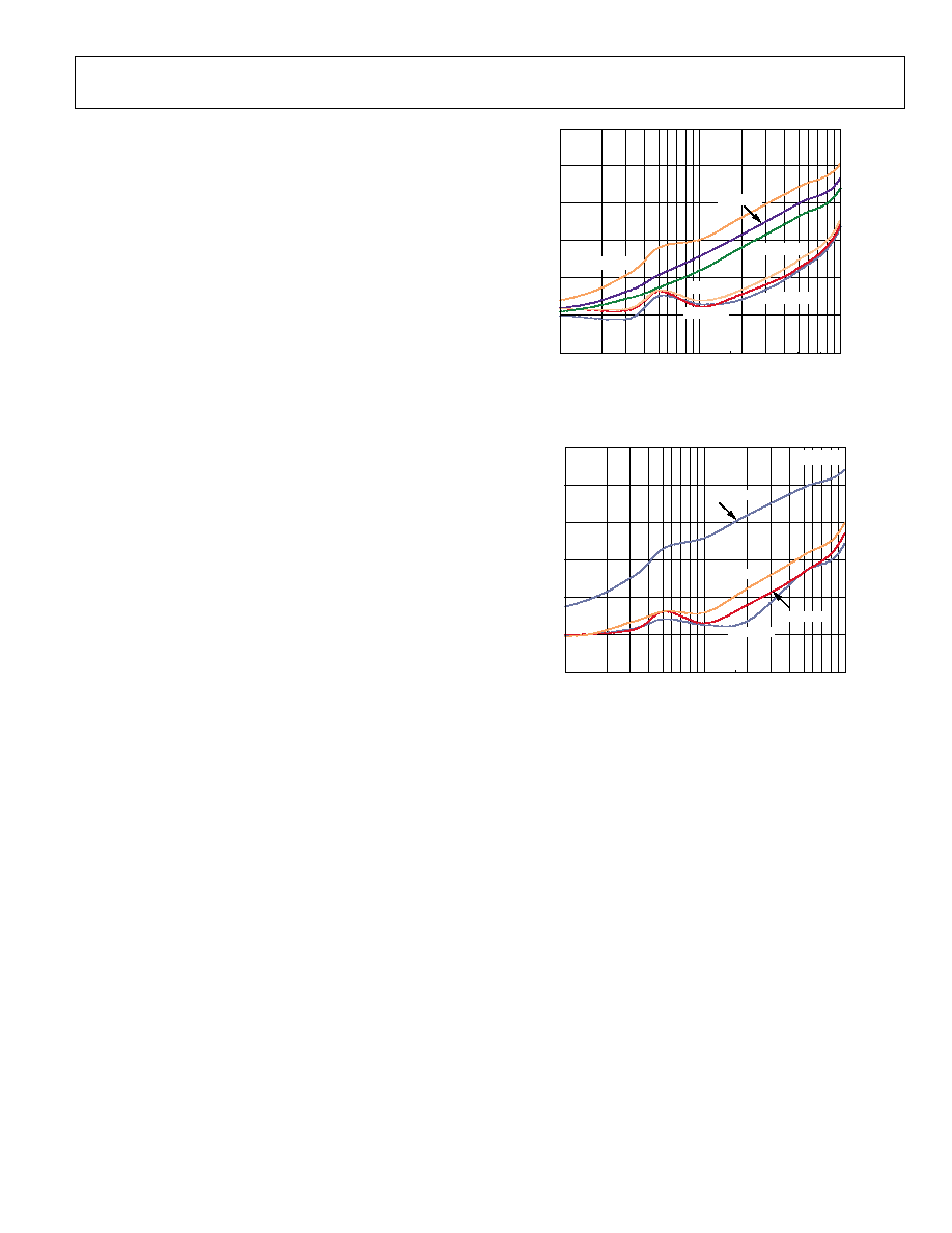
For ac applications, removing high frequency components from
the analog input signal is recommended, by using an RC band-
pass filter on the relevant analog input pin. In applications where
harmonic distortion and signal-to-noise ratio are critical, the
analog input should be driven from a low impedance source.
Large source impedances significantly affect the ac performance
of the ADC. This may necessitate the use of an input buffer
amplifier. The choice of the op amp is a function of the particular
application.
When no amplifier is used to drive the analog input, the source
impedance should be limited to low values. The maximum source
impedance depends on the amount of total harmonic distortion
(THD) that can be tolerated. THD increases as the source imped-
ance increases, and performance degrades. Figure 23 shows the
THD vs. the analog input signal frequency when using supply
voltages of 3 V ± 10% and 5 V ± 10%. Figure 24 shows the THD
vs. the analog input signal frequency for different source
impedances.
100
90
80
70
50
40
THD (dB)
10
1000
INPUT FREQUENCY (kHz)
03473-0-023
100
60
V
DD
= 5.5V
V
DD
= 5V
V
DD
= 4.5V
V
DD
= 3.3V
V
DD
= 3V
V
DD
= 2.7V
Figure 23. THD vs. Analog Input Frequency for Various
Supply Voltages, F
S
= 136 kSPS, Mode 1
100
90
80
70
50
40
THD (dB)
10
1000
INPUT FREQUENCY (kHz)
03473-0-024
100
60
R
IN
= 50
R
IN
= 10
R
IN
= 100
R
IN
= 1000
V
DD
= 5V
Figure 24. THD vs. Analog Input Frequency for Various
Source Impedances for V
DD
= 5 V, 136 kSPS, Mode 1
AD7997/AD7998
Rev. 0 | Page 18 of 32
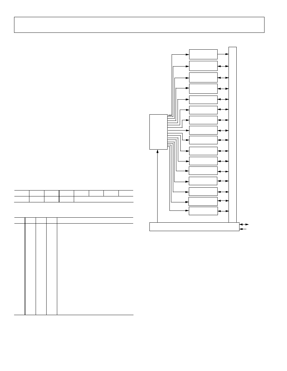
INTERNAL REGISTER STRUCTURE
The AD7997/AD7998 contain 17 internal registers that are used
to store conversion results, high and low conversion limits, and
information to configure and control the device (see Figure 25).
Sixteen are data registers and one is an address pointer register.
Each data register has an address that the address pointer register
points to when communicating with it. The conversion result
register is the only data register that is read only.
ADDRESS POINTER REGISTER
Because it is the register to which the first data byte of every
write operation is written automatically, the address pointer
register does not have and does not require an address. The
address pointer register is an 8-bit register in which the 4 LSBs
are used as pointer bits to store an address that points to one of
the AD7997/AD7998's data registers. The 4 MSBs are used as
command bits when operating in Mode 2 (see the Modes of
Operation section). The first byte following each write address
is to the address pointer register, containing the address of one
of the data registers. The 4 LSBs select the data register to which
subsequent data bytes are written. Only the 4 LSBs of this register
are used to select a data register. On power-up, the address
pointer register contains all 0s, pointing to the conversion result
register.
Table 7. Address Pointer Register
C4 C3 C2 C1 P3 P2 P1 P0
0 0 0 0
Register
Select
Table 8. AD7997/AD7998 Register Addresses
P3 P2 P1 P0 Registers
0
0
0
0
Conversion Result Register (Read)
0
0
0
1
Alert Status Register (Read/Write)
0
0
1
0
Configuration Register (Read/Write)
0
0
1
1
Cycle Timer Register (Read/Write)
0
1
0
0
DATA
LOW
Reg CH1 (Read/Write)
0
1
0
1
DATA
HIGH
Reg CH1 (Read/Write)
0
1
1
0
Hysteresis Reg CH1 (Read/Write)
0
1
1
1
DATA
LOW
Reg CH2 (Read/Write)
1
0
0
0
DATA
HIGH
Reg CH2 (Read/Write)
1
0
0
1
Hysteresis Reg CH2 (Read/Write)
1
0
1
0
DATA
LOW
Reg CH3 (Read/Write)
1
0
1
1
DATA
HIGH
Reg CH3 (Read/Write)
1
1
0
0
Hysteresis Reg CH3 (Read/Write)
1
1
0
1
DATA
LOW
Reg CH4 (Read/Write)
1
1
1
0
DATA
HIGH
Reg CH4 (Read/Write)
1 1 1 1 Hysteresis
Reg
CH4
(Read/Write)
CONFIGURATION
REGISTER
ADDRESS
POINTER
REGISTER
SERIAL BUS INTERFACE
SDA
SCL
D
A
T
A
DATA
LOW
REGISTER CH2
DATA
HIGH
REGISTER CH2
DATA
LOW
REGISTER CH1
HYSTERESIS
REGISTER CH1
DATA
HIGH
REGISTER CH1
CYCLE TIMER
REGISTER
ALERT STATUS
REGISTER
CONVERSION
RESULT REGISTER
HYSTERESIS
REGISTER CH2
DATA
HIGH
REGISTER CH3
DATA
LOW
REGISTER CH3
HYSTERESIS
REGISTER CH3
DATA
HIGH
REGISTER CH4
DATA
LOW
REGISTER CH4
HYSTERESIS
REGISTER CH4
03473-0-025
Figure 25. AD7997/AD7998 Register Structure
AD7997/AD7998
Rev. 0 | Page 19 of 32
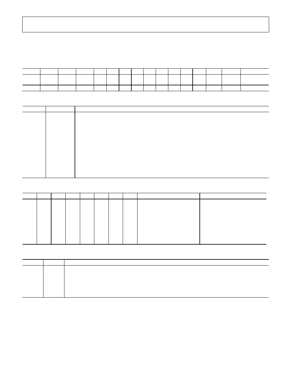
CONFIGURATION REGISTER
The configuration register is a 16-bit read/write register that is used to set the operating mode of the AD7997/AD7998. The 4 MSBs of the
register are unused. The bit functions of all 12 LSBs of the configuration register are outlined in Table 9. A 2-byte write is necessary when
writing to the configuration register.
Table 9. Configuration Register Bits and Default Settings at Power-Up
D15
D14
D13
D12
D11 D10
D9
D8
D7
D6
D5
D4
D3
D2
D1
D0
DONTC
DONTC
DONTC DONTC CH8 CH7 CH6 CH5 CH4 CH3 CH2 CH1 FLTR
ALERT
EN
BUSY/
ALERT
ALERT/BUSY
POLARITY
0
0
0
0
0
0
0
0
0
0
0
0
1
0
0
0
Table 10. Bit Function Descriptions
Bit
Mnemonic
Comment
D11 to D4
CH8 to CH1
These 8-channel address bits select the analog input channel(s) to be converted. A 1 in any of Bits D11 to D4
selects a channel for conversion. If more than one channel bit is set to 1, the AD7997/AD7998 sequence
through the selected channels, starting with the lowest channel. All unused channels should be set to 0. Prior
to initiating a conversion, a channel or channels for conversion must be selected in the configuration register.
D3 FLTR The value written to this bit of the control register determines whether the filtering on SDA and SCL is
enabled or is to be bypassed. If this bit is a 1, then the filtering is enabled; if it is a 0, the filtering is bypassed.
D2 ALERT
EN
The hardware ALERT function is enabled if this bit is set to 1, and disabled if this bit is set to 0. This bit is used
in conjunction with the BUSY/ALERT bit to determine if the ALERT/BUSY pin acts as an ALERT or a BUSY
output (see Table 12).
D1
BUSY/ALERT
This bit is used in conjunction with the ALERT EN bit to determine if the ALERT/ BUSY output, Pin 17, acts as
an ALERT or BUSY output (see Table 12), and if Pin 17 is configured as an ALERT output pin, if it is to be reset.
D0
BUSY/ALERT
POLARITY
This bit determines the active polarity of the ALERT/BUSY pin regardless of whether it is configured as an
ALERT or BUSY output. It is active low if this bit is set to 0, and active high if set to 1.
Table 11. Channel Selection
D11
D10
D9 D8 D7 D6 D5 D4 Selected
Analog
Input
Channel
Comments
0
0
0
0
0
0
0
1
Convert on Channel 1 (V
IN
1)
0
0
0
0
0
0
1
0
Convert on Channel 2 (V
IN
2)
0
0
0
0
0
1
0
0
Convert on Channel 3 (V
IN
3)
0
0
0
0
1
0
0
0
Convert on Channel 4 (V
IN
4)
0
0
0
1
0
0
0
0
Convert on Channel 5 (V
IN
5)
0
0
1
0
0
0
0
0
Convert on Channel 6 (V
IN
6)
0
1
0
0
0
0
0
0
Convert on Channel 7 (V
IN
7)
1
0
0
0
0
0
0
0
Convert on Channel 8 (V
IN
8)
If more than one channel is
selected, the AD7997/AD7998
start converting on the selected
sequence of channels starting with
the lowest channel in the
sequence.
Table 12. ALERT/BUSY Function
D2
D1
ALERT/BUSY Pin Configuration
0
0
Pin does not provide any interrupt signal.
0
1
Pin configured as a BUSY output.
1
0
Pin configured as an ALERT output.
1
1
Resets the ALERT output pin, the Alert_Flag bit in the conversion result register, and the entire alert status register
(if any is active). If 1/1 is written to Bits D2/D1 in the configuration register to reset the ALERT pin, the Alert_Flag bit,
and the alert status register, the contents of the configuration register read 1/0 for D2/D1, respectively, if read back.
AD7997/AD7998
Rev. 0 | Page 20 of 32
CONVERSION RESULT REGISTER
The conversion result register is a 16-bit, read-only register that
stores the conversion result from the ADC in straight binary
format. A 2-byte read is necessary to read data from this register.
Table 13 shows the contents of the first byte to be read from the
AD7997/AD7998, and Table 14 shows the contents of the second
byte to be read.
Table 13. Conversion Value Register (First Read)
D15
D14
D13
D12
D11
D10 D9
D8
Alert_Flag CH
ID2
CH
ID1
CH
ID0
M S B B10
B9
B8
Table 14. Conversion Value Register (Second Read)
D7
D6
D5
D4
D3
D2
D1
D0
B7
B6
B5
B4
B3
B2
B1
B0
The AD7997/AD7998 conversion result consists of an Alert_Flag
bit, three channel identifier bits, and the 10- and 12-bit data
result (MSB first). For the AD7997, the 2 LSBs (D1 and D0) of
the second read contain two 0s. The three channel identification
bits can be used to identify to which of the eight analog input
channels the conversion result corresponds.
The Alert_Flag bit indicates whether the conversion result being
read or any other channel result has violated the limit registers
associated with it. If an ALERT occurs, the master can read the
ALERT status register to obtain more information on where the
ALERT occurred.
LIMIT REGISTERS
The AD7997/AD7998 have four pairs of limit registers. Each
pair stores high and low conversion limits for the first four
analog input channels, CH1 to CH4. Each pair of limit registers
has one associated hysteresis register. All 12 registers are 16 bits
wide; only the 12 LSBs of the registers are used for the AD7997
and AD7998. For the AD7997, the 2 LSBs, D1 and D0 in these
registers, should contain 0s. On power-up, the contents of the
DATA
HIGH
register for each channel is full scale, while the
contents of the DATA
LOW
registers is zero scale by default. The
AD7997/AD7998 signal an alert (in either hardware, software,
or both depending on configuration) if the conversion result
moves outside the upper or lower limit set by the limit registers.
There are no limit registers or hysteresis registers associated
with CH5 to CH8.
DATA
HIGH
Register CH1/CH2/CH3/CH4
The DATA
HIGH
registers for CH1 to CH 4 are 16-bit read/write
registers; only the 12 LSBs of each register are used. This
register stores the upper limit that activates the ALERT output
and/or the Alert_Flag bit in the conversion result register. If the
value in the conversion result register is greater than the value
in the DATA
HIGH
register, an ALERT occurs for that channel.
When the conversion result returns to a value at least N LSBs
below the DATA
HIGH
register value, the ALERT output pin and
Alert_Flag bit are reset. The value of N is taken from the
hysteresis register associated with that channel. The ALERT pin
can also be reset by writing to Bits D2 and D1 in the
configuration register. For the AD7997, D1 and D0 of the
DATA
HIGH
register should contain 0s.
Table 15. DATA
HIGH
Register (First Read/Write)
D15 D14 D13 D12 D11 D10 D9 D8
0
0
0
0
B11
B10
B9
B8
Table 16. DATA
HIGH
Register (Second Read/Write)
D7
D6
D5
D4
D3
D2
D1
D0
B7
B6
B5
B4
B3
B2
B1
B0
DATA
LOW
Register CH1/CH2/CH3/CH4
The DATA
LOW
register for each channel is a 16-bit read/write
register; only the 12 LSBs of each register are used. The register
stores the lower limit that activates the ALERT output and/or
the Alert_Flag bit in the conversion result register. If the value
in the conversion result register is less than the value in the
DATA
LOW
register, an ALERT occurs for that channel. When the
conversion result returns to a value at least N LSBs above the
DATA
LOW
register value, the ALERT output pin and Alert_Flag
bit are reset. The value of N is taken from the hysteresis register
associated with that channel. The ALERT output pin can also be
reset by writing to Bits D2 and D1 in the configuration register.
For the AD7997, D1 to D0 of the DATA
LOW
register should
contain 0s.
Table 17. DATA
LOW
Register (First Read/Write)
D15 D14 D13 D12 D11 D10 D9 D8
0 0 0 0 B11
B10
B9
B8
Table 18. DATA
LOW
Register (Second Read/Write)
D7 D6 D5 D4 D3 D2 D1 D0
B7 B6 B5 B4 B3 B2 B1 B0
AD7997/AD7998
Rev. 0 | Page 21 of 32
Hysteresis Register (CH1/CH2/CH3/CH4)
Each hysteresis register is a 16-bit read/write register, of which
only the 12 LSBs are used. The hysteresis register stores the
hysteresis value, N, when using the limit registers. Each pair of
limit registers has a dedicated hysteresis register. The hysteresis
value determines the reset point for the ALERT pin/Alert_Flag
if a violation of the limits has occurred. For example, if a
hysteresis value of 8 LSBs is required on the upper and lower
limits of Channel 1, the 12-bit word, 0000 0000 0000 1000,
should be written to the hysteresis register of CH1, the address
of which is shown in Table 8. On power-up, the hysteresis
registers contain a value of 2 for the AD7997 and a value of 8
for the AD7998. If a different hysteresis value is required, that
value must be written to the hysteresis register for the channel
in question. For the AD7997, D1 and D0 of the hysteresis
register should contain 0s.
Table 19. Hysteresis Register (First Read/Write)
D15
D14 D13 D12 D11 D10 D9 D8
0 0 0 0 B11
B10
B9
B8
Table 20. Hysteresis Register (Second Read/Write)
D7 D6 D5 D4 D3 D2 D1 D0
B7 B6 B5 B4 B3 B2 B1 B0
Using the Limit Registers to Store Min/Max Conversion
Results for CH1 to CH4
If full scale, that is, all 1s, is written to the hysteresis register for
a particular channel, the DATA
HIGH
and DATA
LOW
registers for
that channel no longer act as limit registers as previously
described, but instead act as storage registers for the maximum
and minimum conversion results returned from conversions on
a channel over any given period of time. This function is useful
in applications where the widest span of actual conversion
results is required rather than using the ALERT to signal that an
intervention is necessary. This function could be useful for
monitoring temperature extremes during refrigerated goods
transportation. It must be noted that on power-up, the contents
of the DATA
HIGH
register for each channel are full scale, while the
contents of the DATA
LOW
registers are zero scale by default.
Therefore, minimum and maximum conversion values being
stored in this way are lost if power is removed or cycled.
ALERT STATUS REGISTER (CH1 TO CH4)
The alert status register is an 8-bit, read/write register that
provides information on an alert event. If a conversion result
activates the ALERT pin or the Alert_Flag bit in the conversion
result register, as described in the Limit Registers section, the
alert status register may be read to gain further information.
The Alert Status Register contains two status bits per channel,
one corresponding to the DATA
HIGH
limit and the other to the
DATA
LOW
limit. The bit with a status of 1 shows where the
violation occurred--that is, on which channel--and whether
the violation occurred on the upper or lower limit. If a second
alert event occurs on the other channel between receiving the
first alert and interrogating the alert status register, the
corresponding bit for that alert event is also set.
The alert status register only contains information for CH1 to
CH4 because these are the only channels with associated limit
registers.
The entire contents of the alert status register can be cleared by
writing 1,1, to Bits D2 and D1 in the configuration register, as
shown in Table 12. This may also be done by writing all 1s to
the alert status register itself. Thus, if the alert status register is
addressed for a write operation, which is all 1s, the contents of
the alert status register are cleared or reset to all 0s.
Table 21. Alert Status Register
D7 D6 D5 D4 D3 D2 D1 D0
CH4
HI
CH4
LO
CH3
HI
CH3
LO
CH2
HI
CH2
LO
CH1
HI
CH1
LO
Table 22. Alert Status Register Bit Function Description
Bit
Mnemonic
If bit is set to 1, violation of...
D0 CH1
LO
DATA
LOW
limit on Channel 1.
No violation if bit is set to 0.
D1 CH1
HI
DATA
HIGH
limit on Channel 1.
No violation if bit is set to 0.
D2 CH2
LO
DATA
LOW
limit on Channel 2.
No violation if bit is set to 0.
D3 CH2
HI
DATA
HIGH
limit on Channel 2.
No violation if bit is set to 0.
D4 CH3
LO
DATA
LOW
limit on Channel 3.
No violation if bit is set to 0.
D5 CH3
HI
DATA
HIGH
limit on Channel 3.
No violation if bit is set to 0.
D6 CH4
LO
DATA
LOW
limit on Channel 4.
No violation if bit is set to 0.
D7 CH4
HI
DATA
HIGH
limit on Channel 4.
No violation if bit is set to 0.
AD7997/AD7998
Rev. 0 | Page 22 of 32
CYCLE TIMER REGISTER
The cycle timer register is an 8-bit, read/write register that
stores the conversion interval value for the automatic cycle
interval mode of the AD7997/AD7998 (see the Modes of
Operation section). D5 to D3 of the cycle timer register are
unused and should contain 0s at all times. On power-up, the
cycle timer register contains all 0s, thus disabling automatic
cycle operation of the AD7997/AD7998. To enable automatic
cycle mode, the user must write to the cycle timer register,
selecting the required conversion interval by programming Bits
D2 to D0. Table 23 shows the structure of the cycle timer
register, while Table 24 shows how the bits in this register are
decoded to provide various automatic sampling intervals.
Table 23. Cycle Timer Register and Defaults at Power-Up
D7
D6
D5 D4 D3 D2
D1
D0
Sample
Delay
Bit Trial
Delay
0
0
0
Cyc
Bit2
Cyc
Bit1
Cyc
Bit0
0
0
0 0 0 0
0
0
Table 24. Cycle Timer Intervals
D2 D1 D0
Typical Conversion Interval
(T
CONVERT
= Conversion Time)
0
0
0
Mode Not Selected
0 0 1
T
CONVERT
× 32
0 1 0
T
CONVERT
× 64
0 1 1
T
CONVERT
× 128
1 0 0
T
CONVERT
× 256
1 0 1
T
CONVERT
× 512
1 1 0
T
CONVERT
× 1024
1 1 1
T
CONVERT
× 2048
SAMPLE DELAY AND BIT TRIAL DELAY
It is recommended that no I
2
C bus activity occurs when a
conversion is taking place. However, if this is not possible, for
example when operating in Mode 2 or Mode 3, then in order to
maintain the performance of the ADC, Bits D7 and D6 in the
cycle timer register are used to delay critical sample intervals
and bit trials from occurring while there is activity on the I
2
C
bus. This results in a quiet period for each bit decision. In
certain cases where there is excessive activity on the interface
lines, this may have the effect of increasing the overall
conversion time. However, if bit trial delays extend longer than
1 µs, the conversion terminates.
When Bits D7 and D6 are both 0, the bit trial and sample
interval delaying mechanism is implemented. The default
setting of D7 and D6 is 0. To turn off both delay mechanisms,
set D7 and D6 to 1.
Table 25. Cycle Timer Register and Defaults at Power-up
D7
D6
D5 D4 D3 D2
D1
D0
Sample
Delay
Bit Trial
Delay
0 0 0
Cyc
Bit 2
Cyc
Bit 1
Cyc
Bit 0
0
0
0 0 0 0
0
0

AD7997/AD7998
Rev. 0 | Page 23 of 32
SERIAL INTERFACE
Control of the AD7997/AD7998 is carried out via the I
2
C-
compatible serial bus. The devices are connected to this bus as
slave devices under the control of a master device, such as the
processor.
SERIAL BUS ADDRESS
Like all I
2
C-compatible devices, the AD7997/AD7998 have a
7-bit serial address. The 3 MSBs of this address for the AD7997/
AD7998 are set to 010. The AD7997/AD7998 come in two
versions, the AD7997-0/AD7997-0 and AD7997-1AD7998-1.
The two versions have three different I
2
C addresses available,
which are selected by either tying the address select pin, AS, to
AGND or V
DD
, or by letting the pin float (see Table 6). By giving
different addresses for the two versions, up to five AD7997/
AD7998 devices can be connected to a single serial bus, or the
addresses can be set to avoid conflicts with other devices on the
bus. (See Table 6.)
The serial bus protocol operates as follows.
The master initiates data transfer by establishing a start
condition, defined as a high-to-low transition on the serial
data line SDA, while the serial clock line, SCL, remains high.
This indicates that an address/data stream follows. All slave
peripherals connected to the serial bus responds to the start
condition and shift in the next eight bits, consisting of a
7-bit address (MSB first) plus an R/W bit that determines the
direction of the data transfer, that is, whether data is written to
or read from the slave device.
The peripheral whose address corresponds to the transmitted
address responds by pulling the data line low during the low
period before the ninth clock pulse, known as the acknowledge
bit. All other devices on the bus remain idle while the selected
device waits for data to be read from or written to it. If the R/W
bit is a 0, the master writes to the slave device. If the R/W bit is a
1, the master reads from the slave device.
Data is sent over the serial bus in sequences of nine clock
pulses, eight bits of data followed by an acknowledge bit from
the receiver of data. Transitions on the data line must occur
during the low period of the clock signal and remain stable
during the high period because a low-to-high transition when
the clock is high may be interpreted as a stop signal.
When all data bytes have been read or written, stop conditions
are established. In write mode, the master pulls the data line
high during the 10th clock pulse to assert a stop condition. In
read mode, the master device pulls the data line high during the
low period before the ninth clock pulse. This is known as No
Acknowledge. The master then takes the data line low during
the low period before the 10th clock pulse, then high during the
10th clock pulse to assert a stop condition.
Any number of bytes of data may be transferred over the serial
bus in one operation, but it is not possible to mix read and write
in one operation, because the type of operation is determined at
the beginning and cannot subsequently be changed without
starting a new operation.
AD7997/AD7998
Rev. 0 | Page 24 of 32
WRITING TO THE AD7997/AD7998
Depending on the register being written to, there are three
different writes for the AD7997/AD7998.
WRITING TO THE ADDRESS POINTER REGISTER
FOR A SUBSEQUENT READ
In order to read from a particular register, the address pointer
register must first contain the address of that register. If it does
not, the correct address must be written to the address pointer
register by performing a single-byte write operation, as shown
in Figure 26. The write operation consists of the serial bus
address followed by the address pointer byte. No data is written
to any of the data registers. A read operation may be subsequently
performed to read the register of interest.
WRITING A SINGLE BYTE OF DATA TO THE ALERT
STATUS REGISTER OR CYCLE REGISTER
The alert status register and cycle register are both 8-bit registers,
so only one byte of data can be written to each. Writing a single
byte of data to one of these registers consists of the serial bus
write address, the chosen data register address written to the
address pointer register, followed by the data byte written to the
selected data register. See Figure 27.
WRITING TWO BYTES OF DATA TO A LIMIT,
HYSTERESIS, OR CONFIGURATION REGISTER
Each of the four limit registers are 16-bit registers, so two bytes
of data are required to write a value to any one of them. Writing
two bytes of data to one of these registers consists of the serial
bus write address, the chosen limit register address written to
the address pointer register, followed by two data bytes written
to the selected data register. See Figure 28.
If the master is write addressing the AD7997/AD7998, it can
write to more than one register without readdressing the ADC.
After the first write operation has completed for the first data
register, during the next byte the master simply writes to the
address pointer byte to select the next data register for a write
operation. This eliminates the need to readdress the device in
order to write to another data register.
SDA
START BY
MASTER
ACK. BY
AD7997/AD7998
ACK. BY
AD7997/AD7998
STOP BY
MASTER
FRAME 1
SERIAL BUS ADDRESS BYTE
FRAME 2
ADDRESS POINTER REGISTER BYTE
1
9
1
9
C4
C3
C2
P2
P1
P0
A0
A1
A2
A3
0
0
SCL
1
C1
P3
03473-0-026
R/W
Figure 26. Writing to the Address Pointer Register to Select a Register for a Subsequent Read Operation
SDA
ACK. BY
AD7997/AD7998
1
1
9
9
C4
C3
C2
P2
P1
P0
R/W
A0
A1
A2
A3
0
0
SCL
1
C1
P3
9
1
9
D7
D6
D5
D2
D1
D0
D4
D3
FRAME 3
DATA BYTE
SCL (CONTINUED)
SDA (CONTINUED)
03473-0-027
START BY
MASTER
ACK. BY
AD7997/AD7998
ACK. BY
AD7997/AD7998
STOP BY
MASTER
FRAME 1
SERIAL BUS ADDRESS BYTE
FRAME 2
ADDRESS POINTER REGISTER BYTE
Figure 27. Single-Byte Write Sequence
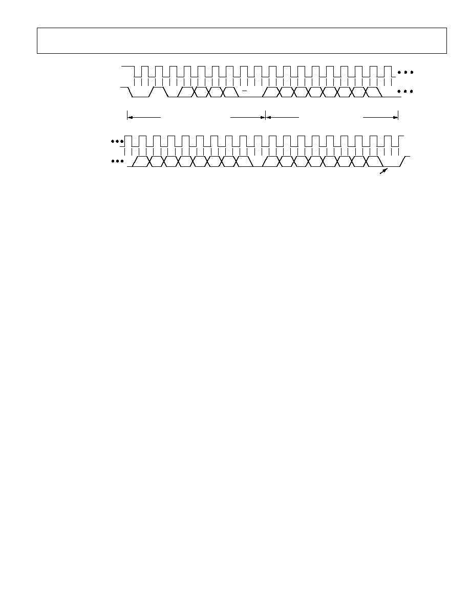
AD7997/AD7998
Rev. 0 | Page 25 of 32
SDA
ACK. BY
AD7997/AD7998
ACK. BY
AD7997/AD7998
1
1
9
9
C4
C3
C2
P2
P1
P0
R/W
A0
A1
A2
A3
0
0
SCL
1
C1
P3
1
9
9
D7
D6
D5
D2
D1/0
D0/0
D4
D3
ACK. BY
AD7997/AD7998
STOP BY
MASTER
LEAST SIGNIFICANT DATA BYTE
MOST SIGNIFICANT DATA BYTE
SCL (CONTINUED)
SDA (CONTINUED)
FRAME 1
SERIAL BUS ADDRESS BYTE
START BY
MASTER
FRAME 2
ADDRESS POINTER REGISTER
9
1
0
0
0
D10
D9
D8
0
D11
ACK. BY
AD7997/AD7998
03473-0-028
Figure 28. 2-Byte Write Sequence
AD7997/AD7998
Rev. 0 | Page 26 of 32
READING DATA FROM THE AD7997/AD7998
Reading data from the AD7997/AD7998 is a 1- or 2-byte
operation. Reading back the contents of the alert status register
or the cycle timer register is a single-byte read operation, as
shown in Figure 29. This assumes the particular register address
has previously been set up by a single-byte write operation to
the address pointer register, as shown in Figure 26. Once the
register address has been set up, any number of reads can be
performed from that particular register without having to write
to the address pointer register again.
If a read from a different register is required, the relevant
register address has to be written to the address pointer register,
and again any number of reads from this register may then be
performed.
Reading data from the configuration register, conversion result
register, DATA
HIGH
registers, DATA
LOW
registers, or hysteresis
registers is a 2-byte operation, as shown in Figure 30. The same
rules apply for a 2-byte read as a single-byte read.
When reading data back from a register, for example the
conversion result register, if more than two read bytes are
supplied, the same or new data is read from the AD7997/
AD7998 without the need to readdress the device. This allows
the master to continuously read from a data register without
having to readdress the AD7997/AD7998.
SDA
1
1
9
9
D7
D6
D5
D2
D1
D0
R/W
A0
A1
A2
A3
0
1
SCL
D4
D3
0
03473-0-029
START BY
MASTER
ACK. BY
AD7997/AD7998
NO ACK. BY
MASTER
STOP BY
MASTER
FRAME 1
SERIAL BUS ADDRESS BYTE
FRAME 2
SINGLE DATA BYTE FROM AD7997/AD7998
Figure 29. Reading a Single Byte of Data from a Selected Register
SDA
1
1
9
9
ALERT
FLAG
CHID2
D10
D9
D8
A0
A1
A2
A3
0
0
SCL
1
D11
1
D7
D6
D5
D2
D1/0
D0/0
D4
D3
SCL (CONTINUED)
SDA (CONTINUED)
CH
ID1
CH
ID0
R/W
03473-0-030
9
START BY
MASTER
ACK. BY
AD7997/AD7998
NO ACK. BY
MASTER
ACK. BY
MASTER
STOP BY
MASTER
FRAME 1
SERIAL BUS ADDRESS BYTE
FRAME 2
MOST SIGNIFICANT DATA BYTE FROM
AD7997/AD7998
FRAME 2
MOST SIGNIFICANT DATA BYTE FROM
AD7997/AD7998
Figure 30. Reading Two Bytes of Data from the Conversion Result Register
AD7997/AD7998
Rev. 0 | Page 27 of 32
ALERT/BUSY PIN
The ALERT/BUSY pin may be configured as an alert output or
as a busy output, as shown in Table 12.
SMBus ALERT
The AD7997/AD7998 ALERT output is an SMBus interrupt line
for devices that want to trade their ability to master for an extra
pin. The AD7997/AD7998 is a slave-only device that uses the
SMBus ALERT to signal the host device that it wants to talk.
The SMBus ALERT on the AD7997/AD7998 is used as an out-
of-range indicator (a limit violation indicator).
The ALERT pin has an open-drain configuration that allows
the ALERT outputs of several AD7997/AD7998s to be wired-
AND'ed together when the ALERT pin is active low. D0 of the
configuration register is used to set the active polarity of the
ALERT output. The power-up default is active low. The ALERT
function can be enabled or disabled by setting D2 of the con-
figuration register to 1 or 0, respectively.
The host device can process the alert interrupt and simultane-
ously access all SMBus alert devices through the alert response
address. Only the device that pulled the alert low acknowledges
the alert response address (ARA). If more than one device pulls
the ALERT pin low, the highest priority (lowest address) device
wins communication rights via standard I
2
C arbitration during
the slave address transfer.
The ALERT output becomes active when the value in the
conversion result register exceeds the value in the DATA
HIGH
register or falls below the value in the DATA
LOW
register for a
selected channel. It is reset when a write operation to the
configuration register sets D1 to a 1, or when the conversion
result returns N LSB below or above the value stored in the
DATA
HIGH
register or the DATA
LOW
register, respectively. N is the
value in the hysteresis register (see the Limit Registers section).
The ALERT output requires an external pull-up resistor that can
be connected to a voltage different from V
DD
provided the maxi-
mum voltage rating of the ALERT output pin is not exceeded.
The value of the pull-up resistor depends on the application, but
should be as large as possible to avoid excessive sink currents at
the ALERT output.
BUSY
When the ALERT/BUSY pin is configured as a BUSY output the
pin is used to indicate when a conversion is taking place. The
polarity of the BUSY pin is programmed through bit D0 in the
Configuration register.
PLACING THE AD7997-1/AD7998-1 INTO
HIGH SPEED MODE
High speed mode communication commences after the master
addresses all devices connected to the bus with the master code,
00001XXX, to indicate that a high speed mode transfer is to
begin. No device connected to the bus is allowed to acknowledge
the high speed master code; therefore, the code is followed by a
not-acknowledge (see Figure 31). The master must then issue a
repeated start followed by the device address with an R/W bit.
The selected device then acknowledges its address.
All devices continue to operate in high speed mode until such a
time as the master issues a stop condition. When the stop condi-
tion is issued, the devices all return to fast mode.
THE ADDRESS SELECT (AS) PIN
The address select pin on the AD7997/AD7998 is used to set
the I
2
C address for the AD7997/AD7998 device. The AS pin can
be tied to V
DD
, to AGND, or left floating. The selection should
be made as close as possible to the AS pin; avoid having long
tracks introducing extra capacitance on to the pin. This is
important for the float selection, as the AS pin has to charge to a
midpoint after the start bit during the first address byte. Extra
capacitance on the AS pin increases the time taken to charge to
the midpoint and may cause an incorrect decision on the device
address. When the AS pin is left floating, the AD7997/AD7998
can work with a capacitive load up to 40 pF.
SDA
ACK. BY
AD7997/AD7998
START BY
MASTER
HS MODE MASTER CODE
SERIAL BUS ADDRESS BYTE
NACK
1
9
1
9
0
1
A2
A1
A0
X
X
1
0
0
0
SCL
0
0
A3
X
Sr
FAST MODE
HIGH SPEED MODE
03473-0-031
Figure 31. Placing the Part into High Speed Mode
AD7997/AD7998
Rev. 0 | Page 28 of 32
MODES OF OPERATION
When supplies are first applied to the AD7997/AD7998, the
ADC powers up in sleep mode and normally remains in this
shutdown state while not converting. There are three methods
of initiating a conversion on the AD7997/AD7998.
MODE 1--USING THE CONVST PIN
A conversion can be initiated on the AD7997/AD7998 by
pulsing the CONVST signal. The conversion clock for the part
is internally generated so no external clock is required, except
when reading from or writing to the serial port. On the rising
edge of CONVST, the AD7997/AD7998 begins to power up (see
point A in Figure 32). The power-up time from shutdown mode
for the AD7997/AD7998 is approximately 1 µs; the CONVST
signal must remain high for 1 µs for the part to power up fully.
CONVST can be brought low after this time. This power-up
time also includes the acquisition time of the ADC. The falling
edge of the CONVST signal places the track-and-hold into hold
mode; a conversion is also initiated at this point (point B in
Figure 32). When the conversion is complete, approximately
2 µs later, the part returns to shutdown (point C in Figure 32)
and remains there until the next rising edge of CONVST. The
master can then read the ADC to obtain the conversion result.
The address pointer register must be pointing to the conversion
result register in order to read back the conversion result.
If the CONVST pulse does not remain high for more than 1 µs,
the falling edge of CONVST still initiates a conversion but the
result is invalid because the AD7997/AD7998 are not fully
powered-up when the conversion takes place. To maintain the
performance of the AD7997/AD7998 in this mode it is
recommended that the I
2
C bus is quiet when a conversion is
taking place.
The cycle timer register and Bits C4 to C1 in the address pointer
register should contain all 0s when operating the AD7997/
AD7998 in this mode. The CONVST pin should be tied low for
all other modes of operation.
To select an analog input channel for conversion in this mode,
the user must write to the configuration register and select the
corresponding channel for conversion. To set up a sequence of
channels to be converted with each CONVST pulse, set the
corresponding channel bits in the configuration register (see
Table 11).
Once a conversion is complete, the master can address the
AD7997/AD7998 to read the conversion result. If further
conversions are required, the SCL line can be taken high while
the CONVST signal is pulsed again; then an additional 18 SCL
pulses are required to read the conversion result.
When operating the AD7997-1/AD7998-1 in Mode 1 and
reading after conversion with a 3.4 MHz f
SCL
, the ADCs can
achieve a typical throughput rate of up to 121 kSPS.
1
1
9
SCA
9
S
7-BIT ADDRESS
R A
FIRST DATA BYTE (MSBs)
A
SECOND DATA BYTE (LSBs)
9
P
SDA
t
POWER-UP
B
A
C
t
CONVERT
03473-0-032
CONVST
A
Figure 32. Mode 1 Operation
AD7997/AD7998
Rev. 0 | Page 29 of 32
MODE 2 COMMAND MODE
This mode allows a conversion to be automatically initiated any
time a write operation occurs. In order to use this mode, the
Command Bits C4 to C1 in the address pointer byte shown in
Table 7 must be programmed.
To select a single analog input for conversion in this mode, the
user must set Bits C4 to C1 of the address pointer byte to
indicate which channel to convert on (see Table 26). When all
four command bits are 0, this mode is not in use.
To select a sequence of channels for conversion in this mode,
first select the channels to be included in the sequence by
setting the channel bits in the configuration register. Next, set
the command bits in the address pointer byte to 0111. With the
command bits of the address pointer byte set to 0111, the ADC
knows to look in the configuration register for the sequence of
channels to be converted. The ADC starts converting on the
lowest channel in the sequence and then the next lowest until all
the channels in the sequence are converted. The ADC stops
converting the sequence when it receives a STOP bit.
Figure 29 illustrates a 2-byte read operation from the
conversion result register. This operation is preceded typically
by a write to the address pointer register so that the following
read accesses the desired register, in this case the conversion
result register (see Figure 26). If Command Bits C4 to C1 are set
when the contents of the address pointer register are being
loaded, the AD7997/AD7998 begins to power up and convert
upon the selected channel(s). Power-up begins on the fifth SCL
falling edge of the address point byte, (see point A in Figure 33).
Table 26 shows the channel selection in this mode via
Command Bits C4 to C1 in the address pointer register. The
wake-up, acquisition, and conversion times combined should
take approximately 3 µs. Following the write operation, the
AD7997/AD7998 must be addressed again to indicate that a
read operation is required. The read then takes place from the
conversion result register. This read accesses the conversion
result from the channel selected via the command bits. If
Command Bits C4 to C1 were set to 0111, and Bits D4 and D5
were set in the configuration register, a 4-byte read would be
necessary. The first read accesses the data from the conversion
on V
IN
1. While this read takes place, a conversion occurs on
V
IN
2. The second read accesses this data from V
IN
2. Figure 34
illustrates how this mode operates; the user would first have
written to the configuration register to select the sequence of
channels to be converted before write addressing the part with
the command bits set to 0111.
When operating the AD7997-1/AD7998-1 in Mode 2 with a
high speed mode, 3.4 MHz SCL, the conversion may not be
complete before the master tries to read the conversion result.
If this is the case, the AD7997-1/AD7998-1 holds the SCL line
low during the ACK clock after the read address, until the con-
version is complete. When the conversion is complete, the
AD7997-1/AD7998-1 releases the SCL line and the master can
then read the conversion result.
After the conversion is initiated by setting the command bits
in the address pointer byte, if the AD7997/AD7998 receives a
STOP or NACK from the master, the AD7997/AD7998 stops
converting.
Table 26. Address Pointer Byte
C4
C3
C2
C1
P3
P2
P1
P0
Mode 2, Convert On
Comments
0
0
0
0
0
0
0
0
Not selected
1
0
0
0
0
0
0
0
V
IN
1
1
0
0
1
0
0
0
0
V
IN
2
1
0
1
0
0
0
0
0
V
IN
3
1
0
1
1
0
0
0
0
V
IN
4
1
1
0
0
0
0
0
0
V
IN
5
1
1
0
1
0
0
0
0
V
IN
6
1
1
1
0
0
0
0
0
V
IN
7
1
1
1
1
0
0
0
0
V
IN
8
0
1
1
1
0
0
0
0
Sequence of channels selected in the
configuration register, Bits D11 to D4.
With the pointer Bits P3P0 set to all 0s,
the next read accesses the results of the
conversion result register.
AD7997/AD7998
Rev. 0 | Page 30 of 32
9
1
1
A
9
S
W A
A
Sr
R
A
A
SECOND DATA BYTE
(LSBs)
FIRST DATA BYTE
(MSBs)
COMMAND/ADDRESS
POINT BYTE
7-BIT ADDRESS
7-BIT ADDRESS
A
SDA
1
1
9
SCL
SDA
SCL
9
9
Sr/P
8
ACK BY
AD7997/AD7998
ACK BY
AD7997/AD7998
ACK BY
MASTER
NACK BY
MASTER
ACK BY
AD7997/AD7998
03473-0-033
Figure 33. Mode 2 Operation
9
1
1
SCL
9
S
7-BIT ADDRESS
W A
COMMAND/ADDRESS
POINT BYTE
A
SDA
FIRST DATA BYTE
(MSBs)
A
SECOND DATA BYTE
(LSBs)
FIRST DATA BYTE
(MSBs)
SECOND DATA BYTE
(LSBs)
A
Sr
7-BIT ADDRESS
R A
SDA
9
9
1
1
SCL
9
8
ACK BY
AD7997/AD7998
ACK BY
AD7997/AD7998
ACK BY
MASTER
ACK BY
MASTER
ACK BY
MASTER
ACK BY
AD7997/AD7998
A
9
9
RESULT FROM CH1
RESULT FROM CH2
A/A
03473-0-034
Figure 34. Mode 2 Sequence Operation
MODE 3--AUTOMATIC CYCLE INTERVAL MODE
An automatic conversion cycle can be selected and enabled by
writing a value to the cycle timer register. A conversion cycle
interval can be set up on the AD7997/AD7998 by programming
the relevant bits in the 8-bit cycle timer register, as decoded in
Table 24. Only the 3 LSBs are used to select the cycle interval;
the 5 MSBs should contain 0s. When the 3 LSBs of the register
are programmed with any configuration other than all 0s, a
conversion takes place every X ms; the cycle interval, X,
depends on the configuration of these three bits in the cycle
timer register. There are seven different cycle time intervals to
choose from, as shown in Table 24. Once the conversion has
taken place, the part powers down again until the next conver-
sion occurs. To exit this mode of operation, the user must
program the 3 LSBs of the cycle timer register to contain all 0s.
To select a channel(s) for operation in the cycle mode, set the
corresponding channel bit(s), D11 to D4, of the configuration
register. If more than one channel bit is set in the configuration
register, the ADC automatically cycles through the channel
sequence starting with the lowest channel and working its way
up through the sequence. Once the sequence is complete, the
ADC starts converting on the lowest channel again, continuing
to loop through the sequence until the cycle timer register
contents are set to all 0s. This mode is useful for monitoring
signals, such as battery voltage and temperature, alerting only
when the limits are violated.
AD7997/AD7998
Rev. 0 | Page 31 of 32
OUTLINE DIMENSIONS
20
1
11
10
6.40 BSC
4.50
4.40
4.30
PIN 1
6.60
6.50
6.40
SEATING
PLANE
0.15
0.05
0.30
0.19
0.65
BSC
1.20 MAX
0.20
0.09
0.75
0.60
0.45
8°
0°
COMPLIANT TO JEDEC STANDARDS MO-153AC
COPLANARITY
0.10
Figure 35. 20-Lead Thin Shrink Small Outline Package [TSSOP]
(RU-20)
Dimensions shown in millimeters
ORDERING GUIDE
Model
1
Temperature Range
Linearity Error
2
(Max)
Package Option
Package Description
AD7997BRU-0
40°C to +85°C
±0.5 LSB
RU-20
TSSOP
AD7997BRU-0REEL
40°C to +85°C
±0.5 LSB
RU-20
TSSOP
AD7997BRUZ-0
3
40°C to +85°C
±0.5 LSB
RU-20
TSSOP
AD7997BRUZ-0REEL
3
40°C to +85°C
±0.5 LSB
RU-20
TSSOP
AD7997BRU-1
40°C to +85°C
±0.5 LSB
RU-20
TSSOP
AD7997BRU-1REEL
40°C to +85°C
±0.5 LSB
RU-20
TSSOP
AD7997BRUZ-1
3
40°C to +85°C
±0.5 LSB
RU-20
TSSOP
AD7997BRUZ-1REEL
3
40°C to +85°C
±0.5 LSB
RU-20
TSSOP
AD7998BRU-0
40°C to +85°C
±1 LSB
RU-20
TSSOP
AD7998BRU-0REEL
40°C to +85°C
±1 LSB
RU-20
TSSOP
AD7998BRUZ-0
3
40°C to +85°C
±1 LSB
RU-20
TSSOP
AD7998BRUZ-0REEL
3
40°C to +85°C
±1 LSB
RU-20
TSSOP
AD7998BRU-1
40°C to +85°C
±1 LSB
RU-20
TSSOP
AD7998BRU-1REEL
40°C to +85°C
±1 LSB
RU-20
TSSOP
AD7998BRUZ-1
3
40°C to +85°C
±1 LSB
RU-20
TSSOP
AD7998BRUZ-1REEL
3
40°C to +85°C
±1 LSB
RU-20
TSSOP
EVAL-AD7997CB
Standalone Evaluation Board
EVAL-AD7998CB
Standalone Evaluation Board
1
The AD7997-0/AD7998-0 support standard and fast I
2
C interface modes. The AD7997-1/AD7998-1 support standard, fast, and high speed I
2
C interface modes.
2
Linearity error here refers to integral nonlinearity.
3
Z = Pb-free part.
RELATED PARTS IN I
2
C-COMPATIBLE ADC PRODUCT FAMILY
Part Number
Resolution
Number of Input Channels
Package
AD7994
12 4 16
TSSOP
AD7993
10 4 16
TSSOP
AD7992
12 2 10
MSOP

AD7997/AD7998
Rev. 0 | Page 32 of 32
NOTES
Purchase of licensed I
2
C components of Analog Devices or one of its sublicensed Associated Companies conveys a license for the purchaser under the Philips I
2
C Patent
Rights to use these components in an I
2
C system, provided that the system conforms to the I
2
C Standard Specification as defined by Philips.
© 2004 Analog Devices, Inc. All rights reserved. Trademarks and
registered trademarks are the property of their respective owners.
D0347309/04(0)
Document Outline