AD7796/AD7797 Low Power, 16-/24-Bit Sigma-Delta ADC for Bridge Sensors Data Sheet (Rev. A)
Low Power, 16-/24-Bit Sigma-Delta ADC
for Bridge Sensors
AD7796/AD7797
Rev. A
Information furnished by Analog Devices is believed to be accurate and reliable. However, no
responsibility is assumed by Analog Devices for its use, nor for any infringements of patents or other
rights of third parties that may result from its use. Specifications subject to change without notice. No
license is granted by implication or otherwise under any patent or patent rights of Analog Devices.
Trademarks and registered trademarks are the property of their respective owners.
One Technology Way, P.O. Box 9106, Norwood, MA 02062-9106, U.S.A.
Tel: 781.329.4700
www.analog.com
Fax: 781.461.3113
©2006 Analog Devices, Inc. All rights reserved.
FEATURES
RMS noise: 65 nV
Instrumentation amp
Temperature sensor
Internal clock oscillator
Simultaneous 50 Hz/60 Hz rejection
Update rate: 4.17 Hz to 123 Hz
Current: 250 A typ
Power-down: 1 A
Power supply: 2.7 V to 5.25 V
40°C to +85°C temperature range
Independent interface power supply
16-lead TSSOP
INTERFACE
3-wire serial
SPI®, QSPITM, MICROWIRETM, and DSP compatible
Schmitt trigger on SCLK
APPLICATIONS
Weigh scales
Strain gages
Industrial process control
Instrumentation
Portable instrumentation
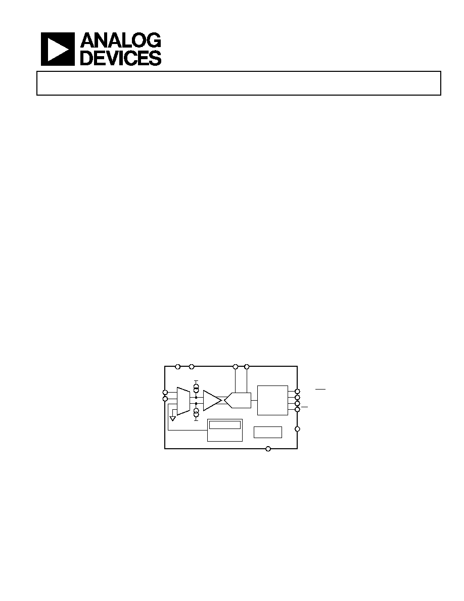
GENERAL DESCRIPTION
The AD7796/AD7797 are complete, analog front ends for high
precision, bridge sensor applications such as weigh scales. The
AD7796/AD7797 contain a - ADC capable of 16-/24-bit
resolution, respectively. The on-chip instrumentation amplifier
has a fixed gain of 128, allowing small amplitude signals such as
those from bridge sensors to be directly interfaced to the ADC.
Each part has one differential input and contains a temperature
sensor that is internally connected to the ADC. This sensor can
be used to perform temperature compensation of the bridge.
The devices can be operated with the internal clock or an
external clock. The output data rate from the parts is software-
programmable and can be varied from 4.17 Hz to 123 Hz.
The AD7796/AD7797 operate with a power supply from 2.7 V
to 5.25 V. Each part consumes a current of 250 A typical and is
housed in a 16-lead TSSOP.
FUNCTIONAL BLOCK DIAGRAM
AD7796/
AD7797
DOUT/RDY
DIN
SCLK
AIN(+)
AIN()
MUX
GND
-
ADC
AV
DD
×128
REFERENCE
TEMP
SENSOR
INTERNAL
CLOCK
GND AV
DD
REFIN()
REFIN(+)
CLK
AD7796: 16-BIT ADC
AD7797: 24-BIT ADC
SERIAL
INTERFACE
AND
CONTROL
LOGIC
CS
DV
DD
06
08
3-
00
1
Figure 1.

AD7796/AD7797
Rev. A | Page 2 of 24
TABLE OF CONTENTS
Features .............................................................................................. 1
Interface ............................................................................................. 1
Applications....................................................................................... 1
General Description ......................................................................... 1
Functional Block Diagram .............................................................. 1
Revision History ............................................................................... 2
Specifications..................................................................................... 3
Timing Characteristics..................................................................... 5
Timing Diagrams.......................................................................... 6
Absolute Maximum Ratings............................................................ 7
Thermal Resistance ...................................................................... 7
ESD Caution.................................................................................. 7
Pin Configuration and Function Descriptions............................. 8
RMS Noise and Resolution Specifications .................................... 9
Typical Performance Characteristics ........................................... 10
On-Chip Registers .......................................................................... 11
Communication Register .......................................................... 11
Status Register ............................................................................. 12
Mode Register ............................................................................. 12
Configuration Register .............................................................. 14
Data Register ............................................................................... 14
ID Register................................................................................... 14
Offset Register ............................................................................ 15
Full-Scale Register...................................................................... 15
ADC Circuit Information.............................................................. 16
Overview ..................................................................................... 16
Digital Interface.......................................................................... 17
Circuit Description......................................................................... 20
Analog Input Channel ............................................................... 20
Bipolar/Unipolar Configuration .............................................. 20
Data Output Coding .................................................................. 20
Reference ..................................................................................... 20
Reset ............................................................................................. 21
Burnout Currents ....................................................................... 21
AV
DD
Monitor ............................................................................. 21
Temperature Monitor ................................................................ 21
Calibration................................................................................... 21
Grounding and Layout .............................................................. 22
Applications..................................................................................... 23
Weigh Scales................................................................................ 23
Outline Dimensions ....................................................................... 24
Ordering Guide .......................................................................... 24
REVISION HISTORY
8/06--Rev. 0 to Rev. A.
Changes to Table 1............................................................................ 3
Changes to Figure 5.......................................................................... 8
Changes to Table 14........................................................................ 13
7/06--Revision 0: Initial Version
AD7796/AD7797
Rev. A | Page 3 of 24
SPECIFICATIONS
AV
DD
= 2.7 V to 5.25 V, DV
DD
= 2.7 V to 5.25 V, GND = 0 V, all specifications T
MIN
to T
MAX
, unless otherwise noted.
Table 1.
Parameter
AD7796B/AD7797B
1
Unit
Test Conditions/Comments
ADC CHANNEL
Output Update Rate
4.17 to 123
Hz nom
No Missing Codes
2
24
Bits min
AD7797 only
16
Bits min
AD7796 only
Resolution
See Table 7 and Table 8
RMS Noise and Update Rates
See Table 6
Integral Nonlinearity
±10
ppm of FSR typ
Offset Error
3 , 4
±1 V
typ
Offset Error Drift vs. Temperature
4
±10 nV/°C
typ
Full-Scale Error
3, 4, 5
±10 V
typ
Gain Drift vs. Temperature
4
±3 ppm/°C
typ
Power Supply Rejection
90
dB min
AIN = 1 V/128
ANALOG INPUTS
Differential Input Voltage Ranges
±V
REF
/128
V nom
V
REF
= REFIN(+) REFIN()
Absolute AIN Voltage Limits
2
GND + 300 mV
V min
AV
DD
- 1.1
V max
Common-Mode Voltage, V
CM
0.5
V min
V
CM
= (AIN(+) + AIN())/2
Analog Input Current
Average Input Current
2
±250
pA max
Update rate < 100 Hz
Average Input Current Drift
±2
pA/°C typ
Normal Mode Rejection
2
Internal Clock
@ 50 Hz, 60 Hz
65
dB min
80 dB typ, 50 ± 1 Hz, 60 ± 1 Hz, FS[3:0] = 1010
6
@ 50 Hz
80
dB min
90 dB typ, 50 ± 1 Hz, FS[3:0] = 1001
6
@ 60 Hz
90
dB min
100 dB typ, 60 ± 1 Hz, FS[3:0] = 1000
6
External Clock
@ 50 Hz, 60 Hz
80
dB min
90 dB typ, 50 ± 1 Hz, 60 ± 1 Hz, FS[3:0] = 1010
6
@ 50 Hz
94
dB min
100 dB typ, 50 ± 1 Hz, FS[3:0] = 1001
6
@ 60 Hz
90
dB min
100 dB typ, 60 ± 1 Hz, FS[3:0] = 1000
6
Common-Mode Rejection
@ DC
90
dB min
AIN = 7.81 mV
@ 50 Hz, 60 Hz
2
90
dB min
50 ± 1 Hz, 60 ± 1 Hz, FS[3:0] = 1010
6
@ 50 Hz, 60 Hz
2
90 dB
min
50 ± 1 Hz (FS[3:0] = 1001
6
), 60 ± 1 Hz,
FS[3:0] = 1000
6
REFERENCE
External REFIN Voltage
2.5
V nom
REFIN = REFIN(+) REFIN()
Reference Voltage Range
2
0.1
V min
AV
DD
V
max
Absolute REFIN Voltage Limits
2
GND - 30 mV
V min
AV
DD
+ 30 mV
V max
Average Reference Input Current
400
nA/V typ
Average Reference Input Current Drift
±0.03
nA/V/°C typ
Normal Mode Rejection
Same as for analog inputs
Common-Mode Rejection
100
dB typ
TEMPERATURE SENSOR
Accuracy
±2
°C typ
Applies if user calibrates the temperature sensor
Sensitivity 0.81
mV/°C
typ
AD7796/AD7797
Rev. A | Page 4 of 24
Parameter
AD7796B/AD7797B
1
Unit
Test Conditions/Comments
INTERNAL/EXTERNAL CLOCK
Internal Clock
Frequency
2
64 ± 3%
kHz min/max
Duty Cycle
50:50
% typ
External Clock
Frequency 64
kHz
nom
A 128 kHz clock can be used if the divide by 2
function is used (Bit CLK1 = CLK0 = 1)
Duty Cycle
45:55 to 55:45
% typ
Applies for external 64 kHz clock (a 128 kHz
clock can have a less stringent duty cycle)
LOGIC INPUTS
CS
2
Input Low Voltage, V
INL
0.8
V
max
DV
DD
= 5 V
0.4
V
max
DV
DD
= 3 V
Input High Voltage, V
INH
2.0
V
min
DV
DD
= 3 V or 5 V
SCLK, CLK, and
DIN (Schmitt-Triggered Input)
2
V
T
(+)
1.4/2
V min/V max
DV
DD
= 5 V
V
T
()
0.8/1.7
V min/V max
DV
DD
= 5 V
V
T
(+) - V
T
()
0.1/0.17
V min/V max
DV
DD
= 5 V
V
T
(+)
0.9/2
V min/V max
DV
DD
= 3 V
V
T
()
0.4/1.35
V min/V max
DV
DD
= 3 V
V
T
(+)
- V
T
()
0.06/0.13
V min/V max
DV
DD
= 3 V
Input Currents
±10
A max
V
IN
= DV
DD
or GND
Input Capacitance
10
pF typ
All digital inputs
LOGIC OUTPUTS (INCLUDING CLK)
Output High Voltage, V
OH
2
DV
DD
- 0.6
V min
DV
DD
= 3 V, I
SOURCE
= 100 A
4
V
min
DV
DD
= 5 V, I
SOURCE
= 200 A
Output Low Voltage, V
OL
2
0.4 V
max
DV
DD
= 3 V, I
SINK
= 100 A
0.4
V
max
DV
DD
= 5 V, I
SINK
= 1.6 mA (DOUT/RDY)/800 A (CLK)
Floating-State Leakage Current
±10
A max
Floating-State Output Capacitance
10
pF typ
Data Output Coding
Offset Binary
SYSTEM CALIBRATION
2
Full-Scale Calibration Limit
+1.05 × FS
V max
Zero-Scale Calibration Limit
-1.05 × FS
V min
Input Span
0.8 × FS
V min
2.1 × FS
V max
POWER REQUIREMENTS
7
Power Supply Voltage
AV
DD
GND
2.7/5.25
V min/max
DV
DD
GND
2.7/5.25
V min/max
Power Supply Currents
I
DD
Current
325
A max
250 A typ @ AV
DD
= 3 V, 280 A typ @ AV
DD
= 5 V
I
DD
(Power-Down Mode)
1
A max
1
Temperature range is 40°C to +85°C.
2
Specification is not production tested, but is supported by characterization data at initial product release.
3
Following a calibration, this error is in the order of the noise for the update rate selected.
4
Recalibration at any temperature removes these errors.
5
Full-scale error applies to both positive and negative full-scale and applies at the factory calibration conditions (AV
DD
= 4 V, T
A
= 25°C).
6
FS[3:0] are the four bits used in the mode register to select the output word rate.
7
Digital inputs equal to DV
DD
or GND.
AD7796/AD7797
Rev. A | Page 5 of 24
TIMING CHARACTERISTICS
AV
DD
= 2.7 V to 5.25 V, DV
DD
= 2.7 V to 5.25 V, GND = 0 V, Input Logic 0 = 0 V, Input Logic 1 = DV
DD
, unless otherwise noted.
Table 2.
Parameter
1 , 2
Limit at T
MIN
, T
MAX
(B Version)
Unit
Conditions/Comments
t
3
100
ns min
SCLK high pulse width
t
4
100
ns min
SCLK low pulse width
Read Operation
t
1
0
ns min
CS falling edge to DOUT/RDY active time
60
ns max
DV
DD
= 4.75 V to 5.25 V
80
ns max
DV
DD
= 2.7 V to 3.6 V
t
2
3
0
ns min
SCLK active edge to data valid delay
4
60
ns max
DV
DD
= 4.75 V to 5.25 V
80
ns max
DV
DD
= 2.7 V to 3.6 V
t
5
5 , 6
10
ns min
Bus relinquish time after CS inactive edge
80
ns max
t
6
0
ns min
SCLK inactive edge to CS inactive edge
t
7
10
ns min
SCLK inactive edge to DOUT/RDY high
Write Operation
t
8
0
ns min
CS falling edge to SCLK active edge setup time
4
t
9
30
ns min
Data valid to SCLK edge setup time
t
10
25
ns min
Data valid to SCLK edge hold time
t
11
0
ns min
CS rising edge to SCLK edge hold time
1
Sample tested during initial release to ensure compliance. All input signals are specified with t
R
= t
F
= 5 ns (10% to 90% of DV
DD
) and timed from a voltage level of 1.6 V.
2
See Figure 3 and Figure 4.
3
These numbers are measured with the load circuit of Figure 2 and defined as the time required for the output to cross the V
OL
or V
OH
limits.
4
SCLK active edge is falling edge of SCLK.
5
These numbers are derived from the measured time taken by the data output to change 0.5 V when loaded with the circuit of Figure 2. The measured number is then
extrapolated back to remove the effects of charging or discharging the 50 pF capacitor. This means that the times quoted in the timing characteristics are the true bus
relinquish times of the parts and, as such, are independent of external bus loading capacitances.
6
RDY returns high after a read of the ADC. In single conversion mode and continuous conversion mode, the same data can be read again, if required, while RDY is high.
Care should be taken to ensure that subsequent reads do not occur close to the next output update. In continuous read mode, the digital word can be read only once.
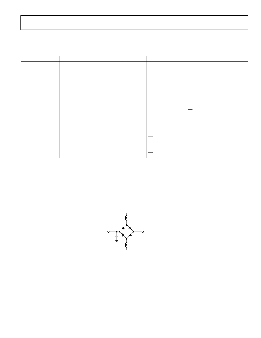
I
SINK
(1.6mA WITH DV
DD
= 5V,
100µA WITH DV
DD
= 3V)
I
SOURCE
(200µA WITH DV
DD
= 5V,
100µA WITH DV
DD
= 3V)
1.6V
TO
OUTPUT
PIN
50pF
06
083
-
0
02
Figure 2. Load Circuit for Timing Characterization
AD7796/AD7797
Rev. A | Page 6 of 24
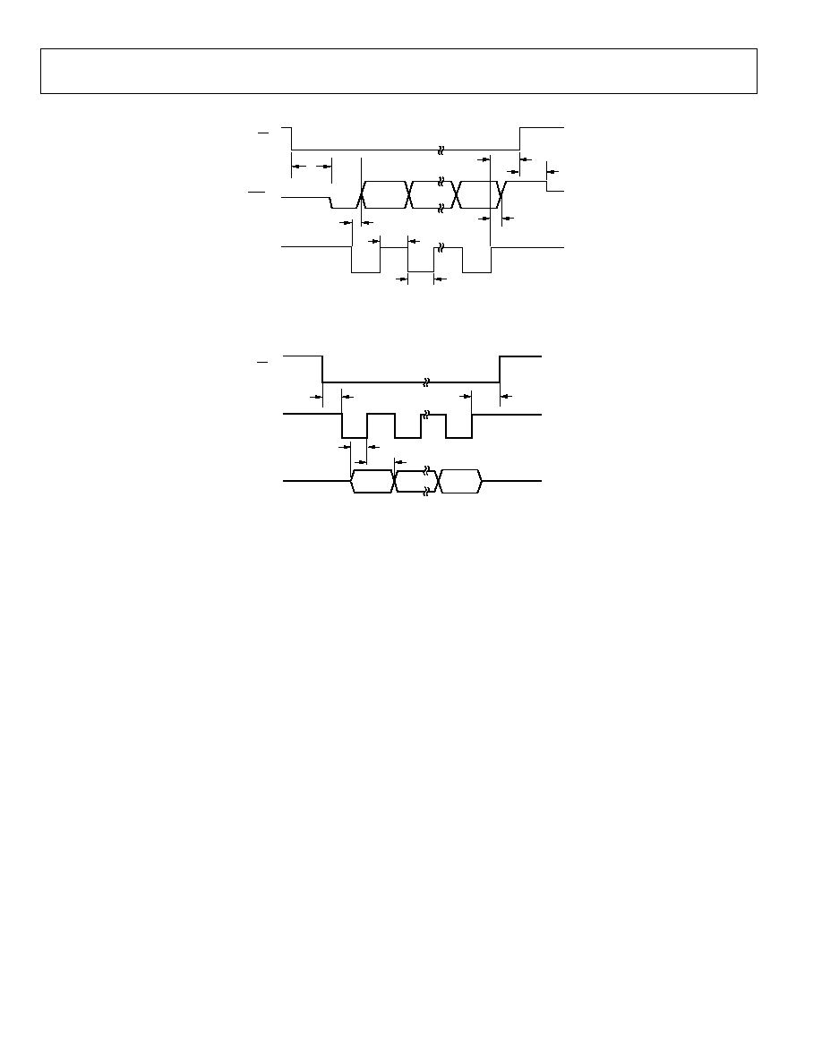
TIMING DIAGRAMS
t
2
t
3
t
4
t
1
t
6
t
5
t
7
CS (I)
DOUT/RDY (O)
SCLK (I)
I = INPUT, O = OUTPUT
MSB
LSB
06
08
3
-
00
3
Figure 3. Read Cycle Timing Diagram
I = INPUT
CS (I)
SCLK (I)
DIN (I)
MSB
LSB
t
8
t
9
t
10
t
11
060
83
-
00
4
Figure 4. Write Cycle Timing Diagram
AD7796/AD7797
Rev. A | Page 7 of 24
ABSOLUTE MAXIMUM RATINGS
T
A
= 25°C, unless otherwise noted.
Table 3.
Parameter
Rating
AV
DD
to GND
-0.3 V to +7 V
DV
DD
to GND
-0.3 V to +7 V
Analog Input Voltage to GND
-0.3 V to AV
DD
+ 0.3 V
Reference Input Voltage to GND
-0.3 V to AV
DD
+ 0.3 V
Digital Input Voltage to GND
-0.3 V to DV
DD
+ 0.3 V
Digital Output Voltage to GND
-0.3 V to DV
DD
+ 0.3 V
AIN/Digital Input Current
10 mA
Operating Temperature Range
-40°C to +85°C
Storage Temperature Range
-65°C to +150°C
Maximum Junction Temperature
150°C
Lead Temperature, Soldering
Vapor Phase (60 sec)
215°C
Infrared (15 sec)
220°C
Stresses above those listed under Absolute Maximum Ratings
may cause permanent damage to the device. This is a stress
rating only; functional operation of the device at these or any
other conditions above those indicated in the operational
section of this specification is not implied. Exposure to absolute
maximum rating conditions for extended periods may affect
device reliability.
THERMAL RESISTANCE
JA
is specified for the worst-case conditions, that is, a device
soldered in a circuit board for surface-mount packages.
Table 4.
Package Type
JA
JC
Unit
TSSOP 128
14
°C/W
ESD CAUTION
AD7796/AD7797
Rev. A | Page 8 of 24
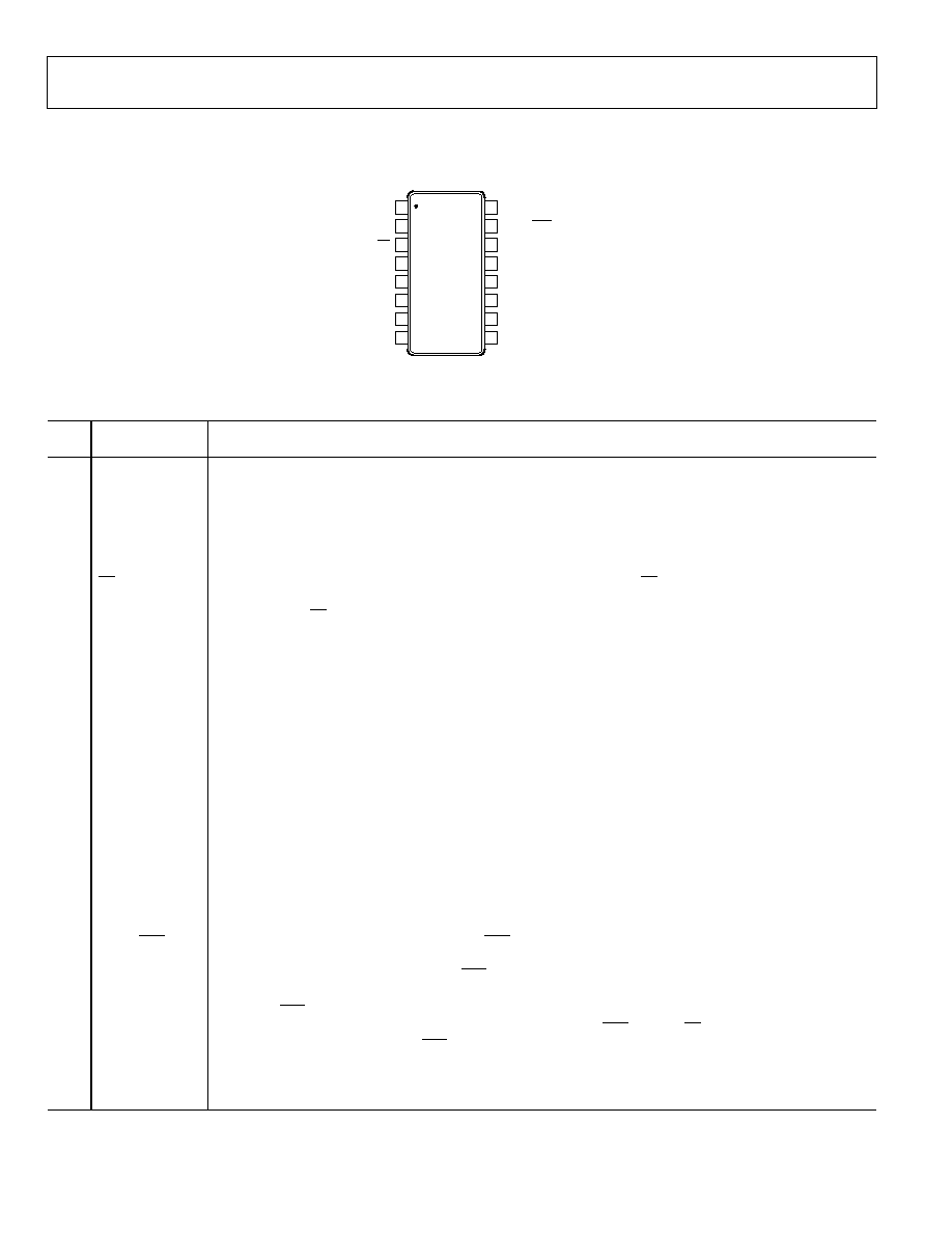
PIN CONFIGURATION AND FUNCTION DESCRIPTIONS
NC = NO CONNECT
1
2
3
4
5
6
7
8
CLK
CS
NC
NC
AIN()
AIN(+)
SCLK
NC
16
15
14
13
12
11
10
9
DOUT/RDY
DV
DD
AV
DD
REFIN()
REFIN(+)
NC
GND
DIN
TOP VIEW
(Not to Scale)
AD7796/
AD7797
06
08
3-
00
5
Figure 5. Pin Configuration
Table 5. Pin Function Descriptions
Pin
No.
Mnemonic
Description
1 SCLK
Serial Clock Input. This serial clock input is for data transfers to and from the ADC. The SCLK has a Schmitt-
triggered input, making the interface suitable for opto-isolated applications. The serial clock can be continuous
with all data transmitted in a constant train of pulses. Alternatively, it can be a noncontinuous clock with the
information being transmitted to or from the ADC in smaller batches of data.
2
CLK
Clock In/Clock Out. The internal clock can be made available at this pin. Alternatively, the internal clock can be
disabled, and the ADC can be driven by an external clock. This allows several ADCs to be driven from a common
clock, allowing simultaneous conversions to be performed.
3
CS
Chip Select Input. This is an active low logic input used to select the ADC. CS can be used to select the ADC in
systems with more than one device on the serial bus or as a frame synchronization signal in communicating
with the device. CS can be hardwired low, allowing the ADC to operate in 3-wire mode with SCLK, DIN, and
DOUT used to interface with the device.
4
NC
No Connect.
5
AIN(+)
Analog Input. AIN(+) is the positive terminal of the differential analog input pair AIN(+)/AIN(-).
6
AIN(-)
Analog Input. AIN(-) is the negative terminal of the differential analog input pair AIN(+)/AIN(-).
7
NC
No Connect.
8
NC
No Connect.
9
REFIN(+)
Positive Reference Input/Analog Input. An external reference can be applied between REFIN(+) and REFIN().
REFIN(+) can lie anywhere between AV
DD
and GND + 0.1 V. The nominal reference voltage (REFIN(+) REFIN(-)) is
2.5 V, but the parts function with a reference of 0.1 V to AV
DD
.
10
REFIN(-)
Negative Reference Input/Analog Input. REFIN(-) is the negative reference input for REFIN. This reference input
can lie anywhere between GND and AV
DD
- 0.1 V.
11
NC
No Connect.
12
GND
Ground Reference Point.
13
AV
DD
Supply Voltage, 2.7 V to 5.25 V.
14
DV
DD
Digital Interface Supply Voltage. The logic levels for the serial interface pins are related to this supply, which is
between 2.7 V and 5.25 V. The DV
DD
voltage is independent of the voltage on AV
DD
; therefore, AV
DD
can equal 5 V
with DV
DD
at 3 V or vice versa.
15
DOUT/RDY
Serial Data Output/Data Ready Output. DOUT/RDY serves a dual purpose. It functions as a serial data output pin
to access the output shift register of the ADC. The output shift register can contain data from any of the on-chip
data or control registers. In addition, DOUT/RDY operates as a data ready pin, going low to indicate the completion
of a conversion. If the data is not read after the conversion, the pin goes high before the next update occurs.
The DOUT/RDY falling edge can be used as an interrupt to a processor, indicating that valid data is available.
With an external serial clock, the data can be read using the DOUT/RDY pin. With CS low, the data/control word
information is placed on the DOUT/RDY pin on the SCLK falling edge and is valid on the SCLK rising edge.
16
DIN
Serial Data Input. This serial data input accesses the input shift register on the ADC. Data in this shift register is
transferred to the control registers within the ADC; the register selection bits of the communication register
identify the appropriate register.
AD7796/AD7797
Rev. A | Page 9 of 24
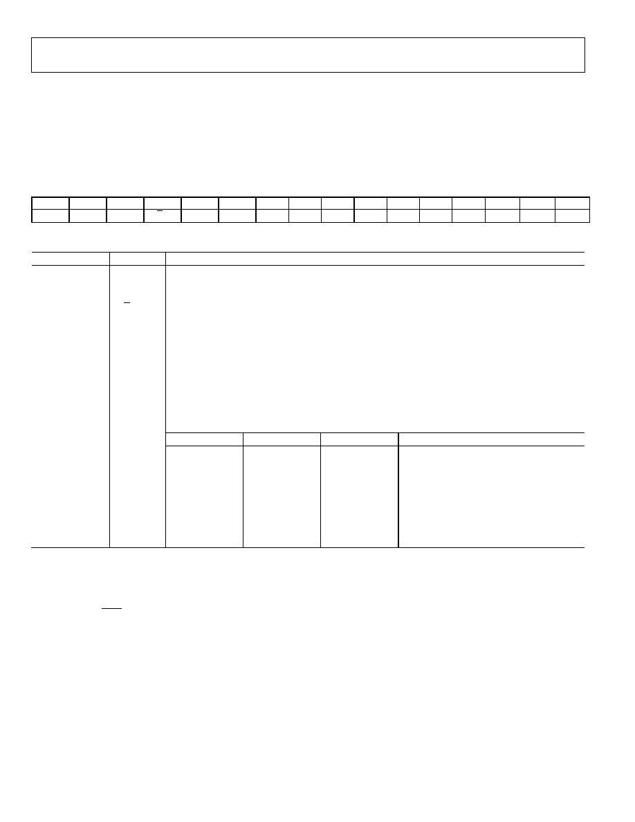
RMS NOISE AND RESOLUTION SPECIFICATIONS
Table 6 shows the rms noise of the AD7796/AD7797 for some
of the update rates. The numbers given are for the bipolar input
range with an external 2.5 V reference. These numbers are
typical and are generated with a differential input voltage of 0 V.
Table 7 and Table 8 show the effective resolution, while the
output peak-to-peak (p-p) resolution is shown in brackets. It is
important to note that the effective resolution is calculated
using the rms noise, while the p-p resolution is based on the p-p
noise. The p-p resolution represents the resolution for which
there is no code flicker. These numbers are typical and are
rounded to the nearest 0.5 LSB.
Table 6. RMS Noise (V) vs. Output Update Rate for the
AD7796/AD7797 Using a 2.5 V Reference
Update Rate (Hz)
RMS Noise (V)
4.17
0.065
6.25
0.07
8.33
0.08
10
0.09
12.5
0.1
16.7
0.12
33.2
0.17
50
0.21
62
0.23
123
0.43
Table 7. Typical Resolution (Bits) vs. Output Update Rate for
the AD7797 Using a 2.5 V Reference
Update Rate (Hz)
Effective Bits (p-p)
4.17
19 (16.5)
6.25
19 (16.5)
8.33
19 (16)
10
18.5 (16)
12.5
18.5 (16)
16.7
18.5 (15.5)
33.2
18 (15)
50
17.5 (15)
62
17.5 (14.5)
123
16.5 (13.5)
Table 8. Typical Resolution (Bits) vs. Output Update Rate for
the AD7796 Using a 2.5 V Reference
Update Rate (Hz)
Effective Bits (p-p)
4.17
16 (16)
6.25
16 (16)
8.33
16 (16)
10
16 (16)
12.5
16 (16)
16.7
16 (15.5)
33.2
16 (15)
50
16 (15)
62
16 (14.5)
123
16 (13.5)
AD7796/AD7797
Rev. A | Page 10 of 24
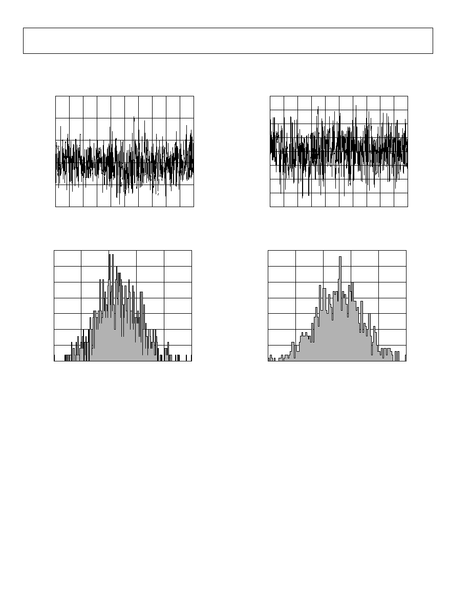
SAMPLES
(µ
V
)
TYPICAL PERFORMANCE CHARACTERISTICS
60
40
0
1000
2.0
2.0
0
1000
SAMPLES
(µ
V
)
40
20
0
20
100
200
300
400
500
600
700
800
900
0
608
3-
0
06
Figure 6. AD7797 Noise (V
REF
= AV
DD
, Update Rate = 16.7 Hz)
17.5
0
8388485
8388744
CODE
O
C
CURR
E
NC
E
15.0
12.5
10.0
7.5
5.0
2.5
8388550
8388600
8388650
8388700
0
608
3-
0
07
Figure 7. AD7797 Noise Distribution Histogram
(V
REF
= AV
DD
, Update Rate = 16.7 Hz)
100
200
300
400
500
600
700
800
900
1.5
1.0
0.5
0
0.5
1.0
1.5
0
608
3-
0
08
Figure 8. AD7797 Noise (V
REF
= AV
DD
, Update Rate = 4.17 Hz)
35
0
8388553
8388662
CODE
O
C
CURR
E
NC
E
8388580
8388600
8388620
8388640
30
25
20
15
10
5
0
608
3-
0
09
Figure 9. AD7797 Noise Distribution Histogram
(V
REF
= AV
DD
, Update Rate = 4.17 Hz)
AD7796/AD7797
Rev. A | Page 11 of 24
ON-CHIP REGISTERS
The ADC is controlled and configured via a number of on-chip
registers, which are described on the following pages. In the
following descriptions, set implies a Logic 1 State and cleared
implies a Logic 0 State, unless otherwise stated.
COMMUNICATION REGISTER
RS2, RS1, RS0 = 0, 0, 0
The communication register is an 8-bit write-only register. All
communication to the part must start with a write operation to
this register. The data written to the communication register
determines whether the next operation is a read or write opera-
tion, and selects the register where this operation takes place.
Once the subsequent read or write operation to the selected
register is complete, the interface returns to where it expects a
write operation to the communication register (this is the
default state of the interface). On power-up or after a reset, the
ADC is in this default state waiting for a write operation to the
communication register. In situations where the interface
sequence is lost, a write operation of at least 32 serial clock
cycles with DIN high returns the ADC to this default state by
resetting the entire part. Table 9 outlines the bit designations for
the communication register. CR0 through CR7 indicate the bit
location, with CR denoting that the bits are in the communication
register. CR7 denotes the first bit of the data stream. The number
in brackets indicates the power-on/reset default status of that bit.
MSB
LSB
CR7
CR6
CR5
CR4
CR3
CR2
CR1
CR0
WEN(0)
R/W(0)
RS2(0)
RS1(0)
RS0(0)
CREAD(0)
0(0)
0(0)
Table 9. Communication Register Bit Designations
Bit Location Bit Name
Description
CR7
WEN
Write Enable Bit. A 0 must be written to this bit first to ensure that a write to the communication register
occurs. If a 1 is the first bit written, the part does not clock onto subsequent bits in the register; it stays at this
bit location until a 0 is written. Once a 0 is written to the WEN bit, the next seven bits are loaded to the
communication register.
CR6
R/W
A 0 in this bit location indicates that the next operation is a write to a specified register. A 1 in this position
indicates that the next operation is a read from the designated register.
CR5 to CR3
RS2 to RS0 Register Address Bits. These address bits determine which ADC registers are being selected during this serial
interface communication. See Table 10.
CR2
CREAD
Continuous Read of the Data Register. When this bit is set to 1 (and the data register is selected), the serial
interface is configured to continuously read the data register. For example, the contents of the data register are
automatically placed on the DOUT pin when the SCLK pulses are applied and after the RDY pin goes low. This
indicates that a conversion is complete. The communication register does not have to be written to for data reads.
To enable continuous read mode, the instruction 01011100 must be written to the communication register.
To exit the continuous read mode, the instruction 01011000 must be written to the communication register
while the RDY pin is low. While in continuous read mode, the ADC monitors activity on the DIN line so it can
receive the instruction to exit continuous read mode. Additionally, a reset occurs if 32 consecutive 1s are seen
on DIN. Therefore, DIN should be held low in continuous read mode until an instruction is written to the device.
CR1 to CR0
0
These bits must be programmed to Logic 0 for correct operation.
Table 10. Register Selection
RS2
RS1
RS0
Register
Register Size
0
0
0
Communication Register During a Write Operation
8 bits
0
0
0
Status Register During a Read Operation
8 bits
0
0
1
Mode Register
16 bits
0
1
0
Configuration Register
16 bits
0
1
1
Data Register
16 bits (AD7796), 24 bits (AD7797)
1
0
0
ID Register
8 bits
1
0
1
Reserved
8 bits
1
1
0
Offset Register
16 bits (AD7796), 24 bits (AD7797)
1
1
1
Full-Scale Register
16 bits (AD7796), 24 bits (AD7797)
AD7796/AD7797
Rev. A | Page 12 of 24
STATUS REGISTER
RS2, RS1, RS0 = 0, 0, 0; Power-On/Reset = 0x80
The status register is an 8-bit read-only register. To access the ADC status register, the user must write to the communication register,
select the next operation to be a read, and load Bit RS2, Bit RS1, and Bit RS0 with 0. Table 11 outlines the bit designations for the status
register. SR0 through SR7 indicate the bit locations, with SR denoting that the bits are in the status register. SR7 denotes the first bit of the
data stream. The number in brackets indicates the power-on/reset default status of that bit.
MSB
LSB
SR7
SR6
SR5
SR4
SR3
SR2
SR1
SR0
RDY(1)
ERR(0)
0(0)
0(0)
0(0)
CH2(0)
CH1(0)
CH0(0)
Table 11. Status Register Bit Designations
Bit Location Bit Name
Description
SR7
RDY
Ready Bit for ADC. Cleared when data is written to the ADC data register. Set automatically after the ADC data
register has been read or before the data register is updated with a new conversion result to indicate to the
user not to read the conversion data. It is also set when the part is placed in power-down mode. DOUT/RDY
also indicates the end of a conversion and can be used as an alternative to the status register for monitoring
the ADC for conversion data.
SR6
ERR
ADC Error Bit. This bit is written to at the same time as the RDY bit. Set to indicate that the result written to the
ADC data register has been clamped to all 0s or all 1s. Error sources include overrange and underrange.
Cleared by a write operation to start a conversion.
SR5 to SR3
0
These bits are automatically cleared.
SR2 to SR0
CH2 to CH0 These bits indicate the channel that is being converted by the ADC.
MODE REGISTER
RS2, RS1, RS0 = 0, 0, 1; Power-On/Reset = 0x000A
The mode register is a 16-bit read/write register. This register is used to select the operating mode, update rate, and clock source. Table 12
outlines the bit designations for this register. MR0 through MR15 indicate the bit locations, with MR denoting that the bits are in the
mode register. MR15 denotes the first bit of the data stream. The number in brackets indicates the power-on/reset default status of that
bit. Any write to the setup register resets the modulator and filter, and sets the RDY bit.
MSB
LSB
MR15
MR14
MR13
MR12
MR11
MR10
MR9
MR8
MR7
MR6
MR5
MR4
MR3
MR2
MR1
MR0
MD2(0)
MD1(0)
MD0(0)
0(0)
0(0)
0(0)
0(0)
0(0)
CLK1(0)
CLK0(0)
0(0)
0(0)
FS3(1)
FS2(0)
FS1(1)
FS0(0)
Table 12. Mode Register Bit Designations
Bit Location
Bit Name
Description
MR15 to MR13 MD2 to MD0 Mode Select Bits. These bits select the operational mode of the AD7796/AD7797 (see Table 13).
MR12 to MR8
0
These bits must be programmed with a Logic 0 for correct operation.
MR7 to MR6
CLK1 to CLK0 These bits are used to select the clock source for the AD7796/AD7797. Either an on-chip 64 kHz clock
or an external clock can be used. The ability to override using an external clock allows several AD7796/
AD7797 devices to be synchronized. In addition, 50 Hz/60 Hz rejection is improved when an accurate
external clock drives the AD7796/AD7797.
CLK1
CLK0
ADC Clock Source
0
0
Internal 64 kHz Clock. Internal clock is not available at the CLK pin.
0
1
Internal 64 kHz Clock. This clock is made available at the CLK pin.
1
0
External 64 kHz Clock Used. An external clock gives better 50 Hz/60 Hz rejection.
See Table 1 for the external clock specifications.
1
1
External Clock Used. The external clock is divided by 2 within the AD7796/AD7797.
MR5 to MR4
0
These bits must be programmed with a Logic 0 for correct operation.
MR3 to MR0
FS3 to FS0
Filter Update Rate Select Bits (see Table 14).
AD7796/AD7797
Rev. A | Page 13 of 24
Table 13. Operating Modes
MD2 MD1 MD0 Mode
0
0
0
Continuous Conversion Mode (default). In continuous conversion mode, the ADC continuously performs
conversions and places the result in the data register. RDY goes low when a conversion is complete. The user can
read these conversions by placing the device in continuous read mode, whereby the conversions are automatically
placed on the DOUT line when SCLK pulses are applied. Alternatively, the user can instruct the ADC to output the
conversion by writing to the communication register. After a power-on, channel change, or write to the mode or
configuration register, the first conversion is available after a period of 2/f
ADC
, while subsequent conversions are
available at a frequency of f
ADC
.
0
0
1
Single Conversion Mode. When single conversion mode is selected, the ADC powers up and performs a single
conversion. The oscillator requires 1 ms to power up and settle. The ADC then performs the conversion, which takes
a time of 2/f
ADC
. The conversion result is placed in the data register, RDY goes low, and the ADC returns to power-
down mode. The conversion remains in the data register and RDY remains active (low) until the data is read or
another conversion is performed.
0
1
0
Idle Mode. In idle mode, the ADC filter and modulator are held in a reset state although the modulator clocks are
still provided.
0
1
1
Power-Down Mode. In power-down mode, all the AD7796/AD7797 circuitry is powered down, including the
burnout currents and CLKOUT circuitry.
1
0
0
Internal Zero-Scale Calibration. An internal short is automatically connected to the channel. A calibration takes
two conversion cycles to complete. RDY goes high when the calibration is initiated and returns low when the
calibration is complete. The ADC is placed in idle mode following a calibration. The measured offset coefficient is
placed in the offset register.
1
0
1
Reserved.
1
1
0
System Zero-Scale Calibration. Users should connect the system zero-scale input to the channel input pins.
A system offset calibration takes two conversion cycles to complete. RDY goes high when the calibration is
initiated and returns low when the calibration is complete. The ADC is placed in idle mode following a calibration.
The measured offset coefficient is placed in the offset register.
1
1
1
System Full-Scale Calibration. Users should connect the system full-scale input to the channel input pins.
A calibration takes two conversion cycles to complete. RDY goes high when the calibration is initiated and returns
low when the calibration is complete. The ADC is placed in idle mode following a calibration. The measured full-
scale coefficient is placed in the full-scale register.
Table 14. Update Rates Available
FS3
FS2
FS1
FS0
f
ADC
(Hz)
t
SETTLE
(ms)
Rejection @ 50 Hz/60 Hz (Internal Clock)
0
0
0
0
X
X
0
0
0
1
X
X
0
0
1
0
X
X
0
0
1
1
123
16
0
1
0
0
62
32
0
1
0
1
50
40
0
1
1
0
X
X
0
1
1
1
33.2
60
1
0
0
0
X
X
1
0
0
1
16.7
120
80 dB (50 Hz only)
1
0
1
0
16.7
120
65 dB (50 Hz and 60 Hz)
1
0
1
1
12.5
160
66 dB (50 Hz and 60 Hz)
1
1
0
0
10
200
69 dB (50 Hz and 60 Hz)
1
1
0
1
8.33
240
70 dB (50 Hz and 60 Hz)
1
1
1
0
6.25
320
72 dB (50 Hz and 60 Hz)
1
1
1
1
4.17
480
74 dB (50 Hz and 60 Hz)
AD7796/AD7797
Rev. A | Page 14 of 24
CONFIGURATION REGISTER
RS2, RS1, RS0 = 0, 1, 0; Power-On/Reset = 0x0710
The configuration register is a 16-bit read/write register. This register is used to configure the ADC for unipolar or bipolar mode, enable
or disable the burnout currents, and select the analog input channel. Table 15 outlines the bit designations for the configuration register.
CON0 through CON15 indicate the bit locations, with CON denoting that the bits are in the configuration register. CON15 denotes the
first bit of the data stream. The number in brackets indicates the power-on/reset default status of that bit.
MSB
LSB
CON15
CON14
CON13
CON12
CON11
CON10
CON9 CON8 CON7 CON6 CON5 CON4 CON3 CON2 CON1 CON0
0(0)
0(0)
BO(0)
U/B(0)
0(0)
1(1)
1(1)
1(1)
0(0)
0(0)
0(0)
1(1)
0(0)
CH2(0)
CH1(0)
CH0(0)
Table 15. Configuration Register Bit Designations
Bit Location
Bit Name
Description
CON15 to CON14 0
These bits must be programmed with a Logic 0 for correct operation.
CON13
BO
Burnout Current Enable Bit. When this bit is set to 1 by the user, the 100 nA current sources in the signal
path are enabled. When BO = 0, the burnout currents are disabled.
CON12
U/B
Unipolar/Bipolar Bit. Set by user to enable unipolar coding, that is, a zero differential input results in
0x0000(00) output, and a full-scale differential input results in 0xFFFF(FF) output. Cleared by the user to
enable bipolar coding. A negative full-scale differential input results in an output code of 0x0000(00), a
zero differential input results in an output code of 0x8000(00), and a positive full-scale differential input
results in an output code of 0xFFFF(FF).
CON11
0
This bit must be programmed with a Logic 0 for correct operation.
CON10 to CON8
1
These bits must be programmed with a Logic 1 for correct operation.
CON7 to CON5
0
These bits must be programmed with a Logic 0 for correct operation.
CON4
1
This bit must be programmed with a Logic 1 for correct operation.
CON3
0
This bit must be programmed with a Logic 0 for correct operation.
CON2 to CON0
CH2 to CH0 Channel Select bits. Written by the user to select the active analog input channel to the ADC.
CH2 CH1 CH0 Channel
0 0 0 AIN(+)
-
AIN()
0 0 1 Reserved
0 1 0 Reserved
0 1 1 AIN()
-
AIN()
1 0 0 Reserved
1 0 1 Reserved
1 1 0 Temp
Sensor
1 1 1 AV
DD
Monitor
DATA REGISTER
RS2, RS1, RS0 = 0, 1, 1; Power-On/Reset = 0x0000 (AD7796)/0x000000 (AD7797)
The conversion result from the ADC is stored in this data register. This is a read-only register. On completion of a read operation from
this register, the RDY bit/pin is set.
ID REGISTER
RS2, RS1, RS0 = 1, 0, 0; Power-On/Reset = 0x5A (AD7796)/0x5B (AD7797)
The identification number for the AD7796/AD7797 is stored in the ID register. This is a read-only register.

AD7796/AD7797
Rev. A | Page 15 of 24
OFFSET REGISTER
RS2, RS1, RS0 = 1, 1, 0; Power-On/Reset = 0x8000 (AD7796)/0x800000 (AD7797)
The analog input channel has an offset register that holds the offset calibration coefficient for the channel. This register is 16 bits wide on
the AD7796 and 24 bits wide on the AD7797, and its power-on/reset value is 0x8000(00). The offset register is used in conjunction with
the full-scale register to form a register pair. The power-on/reset value is automatically overwritten if an internal or system zero-scale
calibration is initiated by the user. The offset register is a read/write register. However, the AD7796/AD7797 must be in idle mode or
power-down mode when writing to this register.
FULL-SCALE REGISTER
RS2, RS1, RS0 = 1, 1, 1; Power-On/Reset = 0x5XXX (AD7796)/0x5XXX00 (AD7797)
The full-scale register is a 16-bit register on the AD7796 and a 24-bit register on the AD7797. The full-scale register holds the full-scale
calibration coefficient for the ADC. The full-scale register is a read/write register. However, when writing to the full-scale register, the
ADC must be placed in power-down mode or idle mode. The full-scale register is configured on power-on with the factory-calibrated
full-scale calibration coefficient. Therefore, every device has a different default coefficient. The default value is automatically overwritten
if a system full-scale calibration is initiated by the user, or if the full-scale register is written to.
AD7796/AD7797
Rev. A | Page 16 of 24
ADC CIRCUIT INFORMATION
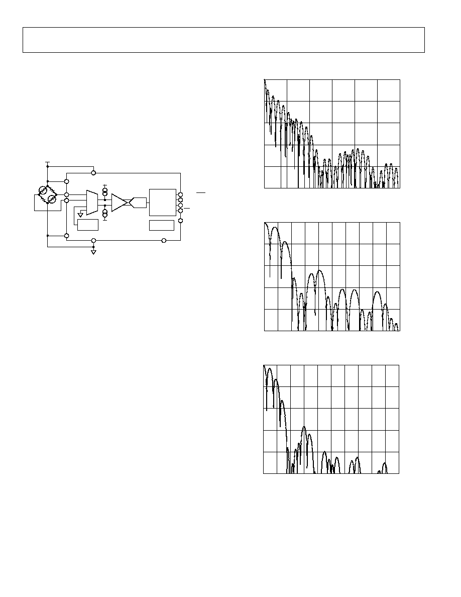
OVERVIEW
The AD7796/AD7797 are low power ADCs that incorporate a
- modulator, in-amp, and an on-chip digital filter intended
for measuring wide dynamic range, low frequency signals, such
as those in pressure transducers and weigh scales.
Each part has one differential input that is buffered. Figure 10
shows the basic connections required to operate the part.
AD7796/AD7797
AIN(+)
AIN()
INTERNAL
CLOCK
AV
DD
DV
DD
REFIN()
REFIN(+)
DOUT/RDY
DIN
SCLK
MUX
GND
GND
CLK
-
ADC
V
DD
V
DD
×128
TEMP
SENSOR
SERIAL
INTERFACE
AND
CONTROL
LOGIC
CS
IN+
IN
OUT
OUT+
06
08
3-
01
0
Figure 10. Basic Connection Diagram
The output rate of the AD7796/AD7797 (f
ADC
) is user-
programmable. The allowable update rates, along with the
corresponding settling times, are listed in Table 14. Normal
mode rejection is the major function of the digital filter.
Simultaneous 50 Hz and 60 Hz rejection is optimized when the
update rate equals 16.7 Hz or less because notches are placed at
both 50 Hz and 60 Hz with these update rates (see Figure 12).
The AD7796/AD7797 use slightly different filter types,
depending on the output update rate used to optimize the
rejection of quantization noise and device noise. When the
update rate is 4.17 Hz to 12.5 Hz, a Sinc
3
filter and an averaging
filter are used. When the update rate is 16.7 Hz to 33.2 Hz,
a modified Sinc
3
filter is used. This filter gives simultaneous
50 Hz/60 Hz rejection when the update rate equals 16.7 Hz.
A Sinc
4
filter is used when the update rate is from 50 Hz to
123 Hz. Figure 11 to Figure 13 show the frequency response of
the different filter types for some of the update rates.
0
20
40
60
80
100
0
1
100
80
60
40
20
FREQUENCY (Hz)
(d
B
)
20
06
08
3-
01
1
Figure 11. Filter Profile with Update Rate = 4.17 Hz
0
20
40
60
80
100
0
2
180
160
140
120
100
80
60
40
20
FREQUENCY (Hz)
(d
B
)
00
06
08
3-
01
2
Figure 12. Filter Profile with Update Rate = 16.7 Hz
0
20
40
60
80
100
0
1000
900
800
700
600
500
400
300
200
100
FREQUENCY (Hz)
(d
B
)
06
08
3-
01
3
Figure 13. Filter Profile with Update Rate = 50 Hz

AD7796/AD7797
Rev. A | Page 17 of 24
DIGITAL INTERFACE
As outlined in the On-Chip Registers section, the AD7796/
AD7797 programmable functions are controlled by a set of on-
chip registers. Data is written to these registers via the part's
serial interface and read access to the on-chip registers is also
provided by this interface. All communication with the part
must start with a write to the communication register. After
power-on or reset, the device expects a write to its
communication register. The data written to this register
determines whether the next operation is a read or a write
operation, and determines the register where this operation
occurs. Therefore, write access to any of the other registers on
the part begins with a write operation to the communication
register followed by a write to the selected register. A read
operation from any other register (except when continuous read
mode is selected) starts with a write to the communication
register followed by a read operation from the selected register.
The serial interface of the AD7796/AD7797 consists of four
signals: CS, DIN, SCLK, and DOUT/RDY. The DIN line is used
to transfer data into the on-chip registers, while DOUT/RDY is
used for accessing from the on-chip registers. SCLK is the serial
clock input for the device, and all data transfers (either on DIN
or DOUT/RDY) occur with respect to the SCLK signal. The
DOUT/RDY pin also operates as a data-ready signal, that is, the
line goes low when a new data-word is available in the output
register. It is reset high when a read operation from the data
register is complete. DOUT/RDY also goes high prior to the
data register update to indicate when not to read from the
device. This ensures that a data read is not attempted while the
register is being updated. CS is used to select a device. It can be
used to decode the AD7796/AD7797 in systems where several
components are connected to the serial bus.
Figure 3 and Figure 4 show timing diagrams for interfacing to
the AD7796/AD7797 with CS being used to decode the part.
Figure 3 shows the timing for a read operation from the
AD7796/AD7797 output shift register, while Figure 4 shows the
timing for a write operation to the input shift register. It is
possible to read the same word from the data register several
times, even though the DOUT/RDY line returns high after the
first read operation. However, care must be taken to ensure that
the read operations have been completed before the next output
update occurs. In continuous read mode, the data register can
be read only once.
The serial interface can operate in 3-wire mode by tying CS low.
In this case, the SCLK, DIN, and DOUT/RDY lines are used
to communicate with the AD7796/AD7797. The end of the
conversion can be monitored using the RDY bit in the status
register. This scheme is suitable for interfacing to micro-
controllers. If CS is required as a decoding signal, it can be
generated from a port pin. For microcontroller interfaces, it is
recommended that SCLK idle high between data transfers.
The AD7796/AD7797 can be operated with CS being used as a
frame synchronization signal. This scheme is useful for DSP
interfaces. In this case, the first bit (MSB) is effectively clocked
out by CS because CS normally occurs after the falling edge of
SCLK in DSPs. The SCLK can continue to run between data
transfers, provided the timing numbers are obeyed.
The serial interface can be reset by writing a series of 1s on the
DIN input. If a Logic 1 is written to the AD7796/AD7797 DIN
line for at least 32 serial clock cycles, the serial interface is reset.
This ensures that the interface can be reset to a known state if
the interface gets lost due to a software error or glitch in the
system. Reset returns the interface to the state where it is
expecting a write to the communication register. This operation
resets the contents of all registers to their power-on values.
Following a reset, the user should allow a period of 500 s
before addressing the serial interface.
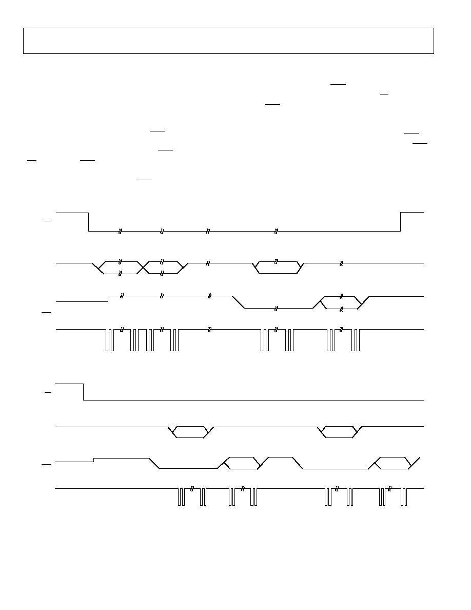
The AD7796/AD7797 can be configured to continuously
convert or to perform a single conversion. See Figure 14
through Figure 16.
AD7796/AD7797
Rev. A | Page 18 of 24
Single Conversion Mode
In single conversion mode, the AD7796/AD7797 are placed in
shutdown mode between conversions. When a single conver-
sion is initiated by setting MD2, MD1, and MD0 in the mode
register to 0, 0, and 1, respectively, the part powers up, performs
a single conversion, and then returns to shutdown mode. The
on-chip oscillator requires 1 ms to power-up. A conversion
requires a time period of 2 × t
ADC
. DOUT/RDY goes low to
indicate the completion of a conversion. When the data-word
has been read from the data register, DOUT/RDY goes high. If
CS is low, DOUT/RDY remains high until another conversion is
initiated and completed. The data register can be read several
times, if required, even when DOUT/RDY has gone high.
Continuous Conversion Mode
This is the default power-up mode. The AD7796/AD7797
continuously convert, and the RDY pin in the status register
goes low each time a conversion is complete. If CS is low, the
DOUT/RDY line also goes low when a conversion is complete.
To read a conversion, the user can write to the communication
register, indicating that the next operation is a read of the data
register. The digital conversion is placed on the DOUT/RDY
pin as soon as SCLK pulses are applied to the ADC. DOUT/RDY
returns high when the conversion is read. The user can read this
register additional times, if required. However, the user must
ensure that the data register is not being accessed at the completion
of the next conversion, or the new conversion word is lost.
0x58
DIN
0x08
0x200A
DATA
SCLK
DOUT/RDY
CS
06
083
-
0
14
Figure 14. Single Conversion
DIN
SCLK
DOUT/RDY
CS
0x58
0x58
DATA
DATA
0
6083
-
0
15
Figure 15. Continuous Conversion
AD7796/AD7797
Rev. A | Page 19 of 24
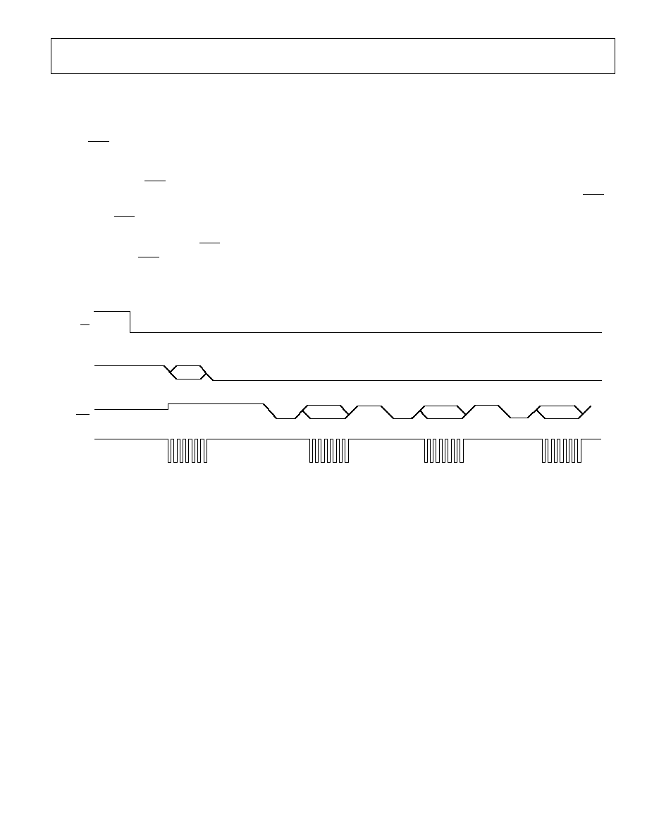
Continuous Read Mode
Rather than write to the communication register each time a
conversion is complete to access the data, the AD7796/AD7797
can be configured to automatically place the conversions on the
DOUT/RDY line. By writing 01011100 to the communication
register, the user need only apply the appropriate number of
SCLK cycles to the ADC. The 16-/24-bit word is automatically
placed on the DOUT/RDY line when a conversion is complete.
The ADC should be configured for continuous conversion mode.
When DOUT/RDY goes low to indicate the end of a conversion,
sufficient SCLK cycles must be applied to the ADC. The data
conversion is placed on the DOUT/RDY line. When the conver-
sion is read, DOUT/RDY returns high until the next conversion
is available. In this mode, the data can be read only once.
The user must also ensure that the data-word is read before the
next conversion is complete. If the user has not read the
conversion before the completion of the next conversion, or if
insufficient serial clocks are applied to the AD7796/AD7797 to
read the word, the serial output register is reset when the next
conversion is complete. The new conversion is placed in the
output serial register.
To exit continuous read mode, the instruction 01011000 must
be written to the communication register while the DOUT/RDY
pin is low. While in continuous read mode, the ADC monitors
activity on the DIN line to receive the instruction to exit the
continuous read mode. Additionally, a reset occurs if 32
consecutive 1s are seen on DIN. Therefore, DIN should be
held low in continuous read mode until an instruction is
written to the device.
DIN
SCLK
DOUT/RDY
CS
0x5C
DATA
DATA
DATA
06
08
3-
01
6
Figure 16. Continuous Read

AD7796/AD7797
Rev. A | Page 20 of 24
CIRCUIT DESCRIPTION
ANALOG INPUT CHANNEL
The AD7796/AD7797 have one differential analog input
channel. The input channel feeds into a high impedance input
stage of the amplifier. Therefore, the input can tolerate signifi-
cant source impedances and is tailored for direct connection to
external resistive-type sensors such as strain gages.
The absolute input voltage range is restricted to a range between
GND + 300 mV and AV
DD
- 1.1 V. Care must be taken in
setting up the common-mode voltage to avoid exceeding these
limits. Otherwise, there is degradation in linearity and noise
performance.
This low noise in-amp means that signals of small amplitude
can be gained within the AD7796/AD7797 while still maintain-
ing excellent noise performance. The amplifier is configured to
have a gain of 128. Therefore, with an external 2.5 V reference,
the unipolar range is 0 mV to 20 mV while the bipolar range is
±20 mV. The common-mode voltage ((AIN(+) + AIN())/2
must be 0.5 V.
BIPOLAR/UNIPOLAR CONFIGURATION
The analog input to the AD7796/AD7797 can accept either
unipolar or bipolar input voltage ranges. A bipolar input range
does not imply that the part can tolerate negative voltages with
respect to system GND. Unipolar and bipolar signals on the
AIN(+) input are referenced to the voltage on the AIN() input.
For example, if AIN(-) is 2.5 V and the ADC is configured for
unipolar mode, the input voltage range on the AIN(+) pin is
2.5 V to 2.02 V.
If the ADC is configured for bipolar mode, the analog input
range on the AIN(+) input is 2.48 V to 2.52 V. The bipolar/
unipolar option is chosen by programming the U/B bit in the
configuration register.
DATA OUTPUT CODING
When the ADC is configured for unipolar operation, the output
code is natural (straight) binary with a zero differential input
voltage resulting in a code of 00...00, a midscale voltage
resulting in a code of 100...000, and a full-scale input voltage
resulting in a code of 111...111. The output code for any analog
input voltage can be represented as
Code = (2
N
× AIN × 128)/V
REF
When the ADC is configured for bipolar operation, the output
code is offset binary with a negative full-scale voltage resulting
in a code of 000...000, a zero differential input voltage resulting
in a code of 100...000, and a positive full-scale input voltage
resulting in a code of 111...111. The output code for any analog
input voltage can be represented as
Code = 2
N 1
× [(AIN × 128 /V
REF
) + 1]
where:
AIN is the analog input voltage
N = 16/24 for the AD7796/AD7797.
REFERENCE
The AD7796/AD7797 have a fully differential input capability
for the channel. The common-mode range for these differential
inputs is GND to AV
DD
. The reference input is unbuffered;
therefore, excessive R-C source impedances introduce gain
errors. The reference voltage REFIN (REFIN(+) - REFIN(-)) is
2.5 V nominal, but the AD7796/AD7797 are functional with
reference voltages 0.1 V to AV
DD
. In applications where the
excitation (voltage or current) for the transducer on the analog
input also drives the reference voltage for the part, the effect of
the low frequency noise in the excitation source is removed
because the application is ratiometric. If the AD7796/AD7797
are used in a nonratiometric application, a low noise reference
should be used.
Recommended 2.5 V reference voltage sources for the AD7796/
AD7797 include the ADR381 and ADR391, which are low
noise, low power references. Also note that the reference
inputs provide a high impedance, dynamic load. Because
the input impedance of each reference input is dynamic,
resistor/capacitor combinations on these inputs can cause
dc gain errors, depending on the output impedance of the
source that is driving the reference inputs.
Reference voltage sources such as those recommended above
(the ADR391, for example) typically have low output
impedances and are, therefore, tolerant to decoupling capacitors
on REFIN(+) without introducing gain errors in the system.
Deriving the reference input voltage across an external resistor
means that the reference input sees a significant external source
impedance. External decoupling on the REFIN pins is not
recommended in this type of circuit configuration.

AD7796/AD7797
Rev. A | Page 21 of 24
RESET
The circuitry and serial interface of the AD7796/AD7797 can
be reset by writing 32 consecutive 1s to the device. This resets
the logic, the digital filter, and the analog modulator, while all
on-chip registers are reset to their default values. A reset is
automatically performed on power-up. When a reset is initiated,
the user must allow a period of 500 s before accessing any of
the on-chip registers. A reset is useful if the serial interface
becomes asynchronous because of noise on the SCLK line.
BURNOUT CURRENTS
The AD7796/AD7797 contain two 100 nA constant current
generators, one sourcing current from AV
DD
to AIN(+) and one
sinking current from AIN() to GND. Both currents are either
on or off, depending on the burnout current enable (BO) bit in
the configuration register. These currents can be used to verify
that an external transducer is still operational before attempting
to take measurements. When the burnout currents are turned
on, they flow in the external transducer circuit, and a measure-
ment of the input voltage on the analog input channel can be
taken. If the resulting voltage is full scale, the user needs to
verify why this is the case. A full-scale reading could mean that
the front-end sensor is open circuit. It could also mean that the
front-end sensor is overloaded and is justified in outputting full
scale, or that the reference could be absent, thus clamping the
data to all 1s.
When reading all 1s from the output, the user needs to check
these three cases before making a judgment. If the voltage
measured is 0 V, it could indicate that the transducer has short
circuited. For normal operation, these burnout currents are
turned off by writing a 0 to the BO bit in the configuration
register.
AV
DD
MONITOR
Along with converting external voltages, the ADC can be used
to monitor the voltage on the AV
DD
pin. When Bit CH2 to
Bit CH0 equal 1, the voltage on the AV
DD
pin is internally
attenuated by 6. The resulting voltage is applied to the
- modulator using an internal 1.17 V reference for analog-to-
digital conversion. This is useful because variations in the
power supply voltage can be monitored.
TEMPERATURE MONITOR
The AD7796/AD7797 have an embedded temperature sensor
that is accessed when Bit CH2 to Bit CH0 are equal to 1, 1, 0,
respectively. When the internal temperature sensor is selected,
the AD7796/AD7797 use an internal 1.17 V reference for
the conversions. The temperature sensor has a sensitivity of
0.81 mV/°C. However, a two-point calibration is required to
optimize the accuracy. The temperature sensor is not factory
calibrated; a user calibration is required. Following a
calibration, the accuracy is 2°C.
CALIBRATION
The AD7796/AD7797 provide three calibration modes that can
be programmed via the mode bits in the mode register. These
are internal zero-scale calibration, system zero-scale calibration,
and system full-scale calibration, which effectively reduces the
offset error and full-scale error to the order of the noise. After
each conversion, the ADC conversion result is scaled using the
ADC calibration registers before being written to the data
register. The offset calibration coefficient is subtracted from the
result prior to multiplication by the full-scale coefficient.
To start a calibration, write the relevant value to the MD2 to
MD0 bits in the mode register. DOUT/RDY goes high when the
calibration is initiated. After the calibration is complete, the
contents of the corresponding calibration registers are updated,
the RDY bit in the status register is set, the DOUT/ RDY pin goes
low (if CS is low), and the AD7796/AD7797 revert to idle mode.
During an internal zero-scale calibration, the zero input is
automatically connected internally to the ADC input pins. A
system calibration, however, expects the system zero-scale and
system full-scale voltages to be applied to the ADC pins before
the calibration mode is initiated. In this way, external ADC
errors are removed.
From an operational point of view, a calibration should be
treated like another ADC conversion. A zero-scale calibration
(if required) should always be performed before a full-scale
calibration. System software should monitor the RDY bit in the
status register or the DOUT/RDY pin to determine the end of
calibration via a polling sequence or an interrupt-driven routine.
Both an internal offset calibration and system offset calibration
takes two conversion cycles. An internal offset calibration is not
needed because the ADC itself removes the offset continuously.
A system full-scale calibration takes two conversion cycles to
complete. The measured full-scale coefficient is placed in the
full-scale register. If system offset calibrations are being
performed along with system full-scale calibrations, the offset
calibration should be performed before the system full-scale
calibration is initiated.

AD7796/AD7797
Rev. A | Page 22 of 24
GROUNDING AND LAYOUT
Because the analog input and reference input of the ADC are
differential, most of the voltages in the analog modulator are
common-mode voltages. The excellent common-mode reject-
ion of the part removes common-mode noise on these inputs.
The digital filter provides rejection of broadband noise on the
power supply, except at integer multiples of the modulator
sampling frequency. The digital filter also removes noise from
the analog and reference inputs provided that these noise
sources do not saturate the analog modulator. As a result, the
AD7796/AD7797 are more immune to noise interference than
conventional high resolution converters. However, because the
resolution of the AD7796/AD7797 is so high, and the noise
levels from the AD7796/AD7797 are so low, care must be taken
with regard to grounding and layout.
The printed circuit board that houses the AD7796/AD7797
should be designed such that the analog and digital sections are
separated and confined to certain areas of the board. A minimum
etch technique is generally best for ground planes because it
gives the best shielding.
It is recommended that the GND pins of the AD7796/AD7797
be tied to the AGND plane of the system. In any layout, it is
important that the user pay attention to the flow of currents in
the system, and ensure that the return paths for all currents are
as close as possible to the paths the currents took to reach their
destinations. Avoid forcing digital currents to flow through the
AGND sections of the layout.
The ground planes of the AD7796/AD7797 should be allowed
to run under the AD7796/AD7797 to prevent noise coupling.
The power supply lines to the AD7796/AD7797 should use as
wide a trace as possible to provide low impedance paths and
reduce the effects of glitches on the power supply line. Fast
switching signals such as clocks should be shielded with digital
ground to avoid radiating noise to other sections of the board,
and clock signals should never be run near the analog inputs.
Avoid crossover of digital and analog signals. Traces on
opposite sides of the board should run at right angles to each
other. This reduces the effects of feedthrough through the
board. A micro-strip technique is by far the best, but it is not
always possible with a double-sided board. In this technique,
the component side of the board is dedicated to ground planes,
while signals are placed on the solder side.
Good decoupling is important when using high resolution
ADCs. AV
DD
should be decoupled with 10 F tantalum in
parallel with 0.1 F capacitors to GND. DV
DD
should be
decoupled with 10 F tantalum in parallel with 0.1 F
capacitors to the system's DGND plane, with the system's
AGND to DGND connection being close to the AD7796/
AD7797. To achieve the best results from these decoupling
components, they should be placed as close as possible to the
device, ideally right up against the device. All logic chips should
be decoupled with 0.1 F ceramic capacitors to DGND.
AD7796/AD7797
Rev. A | Page 23 of 24
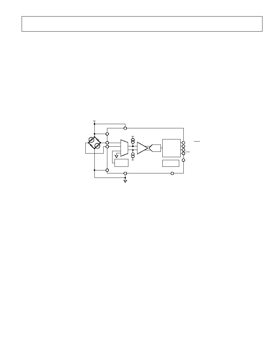
APPLICATIONS
The AD7796/AD7797 offer a high resolution analog-to-digital
function. Because the analog-to-digital function is provided by
a - architecture, the parts are more immune to noisy
environments, making them ideal for use in sensor
measurement, and industrial and process-control applications.
WEIGH SCALES
Figure 17 shows the AD7796/AD7797 being used in a weigh
scale application. The load cell is arranged in a bridge network
and gives a differential output voltage between its OUT+ and
OUT terminals. Assuming a 5 V excitation voltage, the full-
scale output range from the transducer is 10 mV when the
sensitivity is 2 mV/V. The excitation voltage for the bridge can
be used to directly provide the reference for the ADC because
the reference input range includes the supply voltage. This
allows a ratiometric measurement. Therefore, variations of the
excitation voltage do not affect the measurement.
The on-chip temperature sensor can be used for temperature
compensation of the bridge so the variation of the sensor
resistance with temperature drift can be monitored and the
conversions from the bridge can be compensated.
AD7796/AD7797
AIN(+)
AIN()
INTERNAL
CLOCK
AV
DD
DV
DD
REFIN()
REFIN(+)
DOUT/RDY
DIN
SCLK
MUX
GND
GND
CLK
-
ADC
V
DD
V
DD
×128
TEMP
SENSOR
SERIAL
INTERFACE
AND
CONTROL
LOGIC
CS
IN+
IN
OUT
OUT+
06
08
3
-
01
7
Figure 17. Weigh Scales Using the AD7796/AD7797
AD7796/AD7797
Rev. A | Page 24 of 24
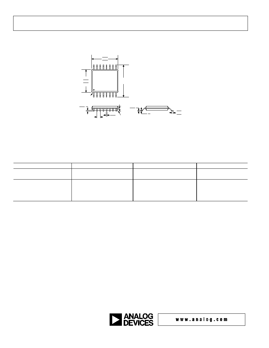
OUTLINE DIMENSIONS
16
9
8
1
PIN 1
SEATING
PLANE
8°
0°
4.50
4.40
4.30
6.40
BSC
5.10
5.00
4.90
0.65
BSC
0.15
0.05
1.20
MAX
0.20
0.09
0.75
0.60
0.45
0.30
0.19
COPLANARITY
0.10
COMPLIANT TO JEDEC STANDARDS MO-153-AB
Figure 18. 16-Lead Thin Shrink Small Outline Package [TSSOP]
(RU-16)
Dimensions shown in millimeters
ORDERING GUIDE
Model
Temperature Range
Package Description
Package Option
AD7796BRUZ
1
40°C to +85°C
16-Lead TSSOP
RU-16
AD7796BRUZ-REEL
1
40°C to +85°C
16-Lead TSSOP
RU-16
AD7797BRUZ
1
40°C to +85°C
16-Lead TSSOP
RU-16
AD7797BRUZ-REEL
1
40°C to +85°C
16-Lead TSSOP
RU-16
EVAL-AD7796EB
Evaluation
Board
EVAL-AD7797EB
Evaluation
Board
1
Z = Pb-free part.
©2006 Analog Devices, Inc. All rights reserved. Trademarks and
registered trademarks are the property of their respective owners.
D06083-0-8/06(A)
Document Outline
- þÿ
- þÿ
- þÿ
- þÿ
- þÿ
- þÿ
- þÿ
- þÿ
- þÿ
- þÿ
- þÿ
- þÿ
- þÿ
- þÿ
- þÿ
- þÿ
- þÿ
- þÿ
- þÿ
- þÿ
- þÿ
- þÿ
- þÿ
- þÿ
- þÿ
- þÿ
- þÿ
- þÿ