
Low Power, 16/24-Bit Sigma-Delta ADC with
Low-Noise In-Amp and Embedded Reference
Preliminary Technical Data
AD7792/AD7793
REV.PrF 6/04.
Information furnished by Analog Devices is believed to be accurate and reliable.
However, no responsibility is assumed by Analog Devices for its use, nor for any
infringements of patents or other rights of third parties that may result from its use.
Specifications subject to change without notice. No license is granted by implication
or otherwise under any patent or patent rights of Analog Devices. Trademarks and
registered trademarks are the property of their respective companies.
One Technology Way, P.O. Box 9106, Norwood, MA 02062-9106, U.S.A.
Tel: 781.329.4700
www.analog.com
Fax: 781.326.8703
© 2004 Analog Devices, Inc. All rights reserved.
FEATURES
Resolution:
AD7792: 16-Bit
AD7793: 24-Bit
Low Noise Programmable Gain Instrumentation-Amp
RMS noise: 80 nV (Gain = 64)
Bandgap Reference with 5ppm/ C Drift typ
Power
Supply: 2.7 V to 5.25 V operation
Normal: 400 µA typ
Power-down: 1 µA max
Update Rate: 4 Hz to 500 Hz
Simultaneous 50 Hz/60 Hz Rejection
Internal Clock Oscillator
Programmable Current Sources (10 µA/200 µA/1 mA)
On-Chip Bias Voltage Generator
100 nA Burnout Currents
Independent Interface Power Supply
16-Lead TSSOP Package
INTERFACE
3-wire serial
SPI®, QSPITM, MICROWIRETM, and DSP compatible
Schmitt trigger on SCLK
APPLICATIONS
Thermocouple Measurements
RTD Measurements
Thermistor Measurements
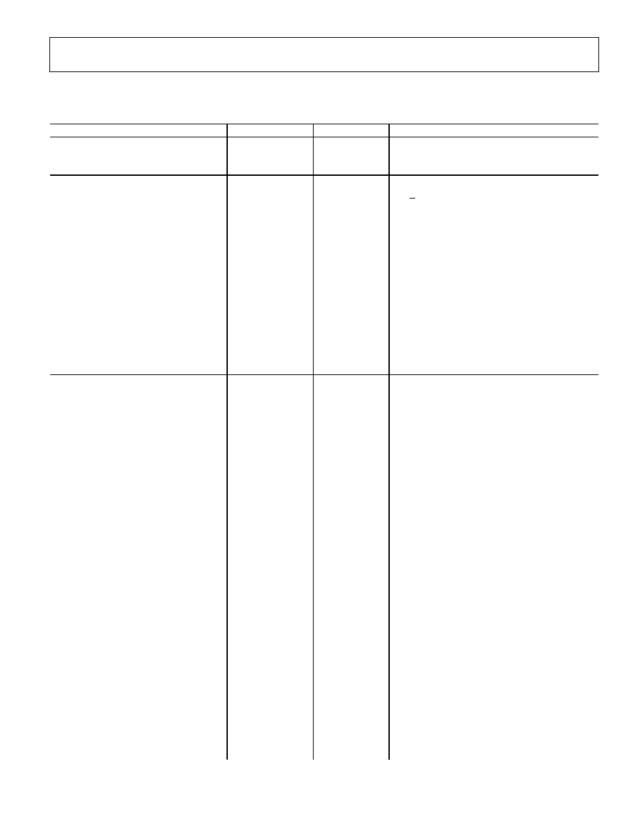
FUNCTIONAL BLOCK DIAGRAM
GND
AVDD
AD7792/AD7793
SERIAL
INTERFACE
AND
CONTROL
LOGIC
INTERNAL
CLOCK
CLK
SIGMA DELTA
ADC
REFIN(+)/AIN3(+)
REFIN(-)/AIN3(-)
BANDGAP
REFERENCE
GND
IN-AMP
VDD
GND
DOUT/RDY
DIN
SCLK
CS
DVDD
AIN1(+)
AIN1(-)
AIN2(+)
AIN2(-)
VDD
IOUT2
VBIAS
IOUT1
MUX
Figure 1.
GENERAL DESCRIPTION
The AD7792/AD7793 is a low power, complete analog front end
for low frequency measurement applications. The
AD7792/AD7793 contains a low noise 16/24-bit - ADC with
three differential analog inputs. The on-chip low noise
instrumentation amplifier means that signals of small
amplitude can be interfaced directly to the ADC. With a gain
setting of 64, the rms noise is 80 nV when the update rate equals
16.6 Hz.
The device contains a precision low noise, low drift internal
bandgap reference for absolute measurements. An external
reference can also be used if ratiometric measurements are re-
quired. On-chip programmable excitation current sources can
be used to supply a constant current to RTDs and thermistors
while the 100 nA burnout currents can be used to ensure that
the sensors connected to the ADC are not burnt out. For ther-
mocouple applications, the on-chip bias voltage generator steps
up the common mode voltage from the thermocouple so that it
is within the ADC's allowable range.
The device can be operated with the internal clock or, alterna-
tively, an external clock can be used if synchronizing several
devices. The output data rate from the part is software pro-
grammable and can be varied from 4 Hz to 500 Hz.
The part operates with a power supply from 2.7 V to 5.25 V. It
consumes a current of 450 uA maximum and is housed in a 16-
lead TSSOP package.

AD7792/AD7793
Preliminary Technical Data
REV.PrF 6/04 | Page 2
TABLE OF CONTENTS
AD7792/AD7793--Specifications.................................................. 3
Timing Characteristics
,
.................................................................... 6
Absolute Maximum Ratings............................................................ 8
Pin Configuration and Function Descriptions............................. 9
Typical Performance Characteristics ........................................... 11
On-chip Registers ........................................................................... 12
Communications Register (RS2, RS1, RS0 = 0, 0, 0) .............. 12
Status Register (RS2, RS1, RS0 = 0, 0, 0; Power-on/Reset =
0x80 (AD7792) / 0x88 (AD7793)) ........................................... 13
Mode Register (RS2, RS1, RS0 = 0, 0, 1; Power-on/Reset =
0x000A)........................................................................................ 13
Configuration Register (rs2, RS1, RS0 = 0, 1, 0; Power-
on/Reset = 0x0710) .................................................................... 15
Data Register (RS2, RS1, RS0 = 0, 1, 1; Power-on/Reset =
0x0000(00)) ................................................................................. 16
ID Register (RS2, RS1, RS0 = 1, 0, 0; Power-on/Reset = 0xXA
(ad7792) / 0xXB (ad7793))........................................................ 16
IO Register (RS2, RS1, RS0 = 1, 0, 1; Power-on/Reset = 0x00)
....................................................................................................... 16
OFFSET Register (RS2, RS1, RS0 = 1, 1, 0; Power-on/Reset =
0x8000(AD7792)/ 0x800000(AD7793)).................................. 17
FULL-SCALE Register (RS2, RS1, RS0 = 1, 1, 1; Power-
on/Reset = 0x5xx5(AD7792)/ 0x5xXXx5(AD7793)) ............ 17
ADC Circuit Information.............................................................. 19
Overview ..................................................................................... 19
Noise Performance ..................................................................... 19
Digital Interface .......................................................................... 20
Single Conversion Mode ....................................................... 21
Continuous Conversion Mode............................................. 21
Continuous Read Mode ........................................................ 22
Circuit Description......................................................................... 23
Analog Input Channel ............................................................... 23
Bipolar/Unipolar Configuration .............................................. 23
Data Output Coding .................................................................. 23
Reference ..................................................................................... 23
V
DD
Monitor ................................................................................ 24
Grounding and Layout .............................................................. 24
Outline Dimensions ....................................................................... 26
ESD Caution................................................................................ 26
REVISION HISTORY
REV.PrF, June 2004: Initial Version
Preliminary Technical Data
AD7792/AD7793
REV.PrF 6/04 | Page 3
AD7792/AD7793--SPECIFICATIONS
1
Table 1. (AV
DD
= 2.7 V to 5.25 V; DV
DD
= 2.7 V to 5.25 V; GND = 0 V; all specifications T
MIN
to T
MAX
, unless otherwise noted.)
Parameter AD7792/AD7793B
Unit Test
Conditions/Comments
ADC CHANNEL SPECIFICATION
Output Update Rate
4
Hz min nom
500
Hz max nom
ADC CHANNEL
No Missing Codes
2
24
Bits
min
f
ADC
< 125 Hz. AD7793
16
Bits
min
Resolution (pk pk)
16
Bits p-p
Gain = 128, 16.6 Hz Update Rate, V
REF
= 2.5V
19
Bits p-p
Gain = 1, 16.6 Hz Update Rate, V
REF
= 2.5V, AD7793
16
Bits p-p
Gain = 1, 16.6 Hz Update Rate, V
REF
= 2.5V, AD7792
Output Noise and Update Rates
See Tables in ADC
Description
Integral Nonlinearity
±15
ppm of FSR max
3.5 ppm of FSR typ, Gain = 1 to 32
±25
ppm of FSR max
5 ppm of FSR typ, Gain = 64 and 128
Offset Error
3
±3
µV
typ
Offset Error Drift vs. Temperature
4
±10
nV/°C
typ
Full-Scale Error
3, 5
±10
µV
typ
Gain Drift vs. Temperature
4
±0.5
ppm/°C typ
Gain = 1 or 2
±3
ppm/°C typ
Gain = 4 to 128
Power Supply Rejection
90
dB min
100 dB typ, AIN = FS/2
ANALOG INPUTS
Differential Input Voltage Ranges
±REFIN/Gain
V nom
REFIN = REFIN(+) REFIN() or Internal Reference,
Gain = 1 to 128
Absolute AIN Voltage Limits
2
Unbuffered Mode
GND 30 mV
V min
Gain = 1 or 2
AV
DD
+ 30 mV
V max
Buffered Mode
GND + 100 mV
V min
Gain = 1 or 2
AV
DD
100 mV
V max
In-Amp Enabled
GND + 300 mV
V min
Gain = 4 to 128
AV
DD
1.1
V max
Common Mode Voltage
0.5
V min
Gain = 4 to 128
Analog Input Current
Buffered Mode or In-Amp Enabled
Average Input Current
2
±200
pA max
Average Input Current Drift
±2
pA/°C typ
Unbuffered Mode
Gain = 1 or 2. Input current varies with input
voltage.
Average Input Current
±400
nA/V typ
Average Input Current Drift
±50
pA/V/°C typ
Normal Mode Rejection
2
Internal Clock
@ 50 Hz, 60 Hz
70
dB min
80 dB typ, 50 ± 1 Hz, 60 ± 1 Hz, FS[3:0] = 1010
6
@ 50 Hz
84
dB min
100 dB typ, 50 ± 1 Hz, FS[3:0] = 1001
6
@ 60 Hz
90
dB min
100 dB typ, 60 ± 1 Hz, FS[3:0] = 1000
6
External Clock
@ 50 Hz, 60 Hz
80
dB min
90 dB typ, 50 ± 1 Hz, 60 ± 1 Hz, FS[3:0] = 1010
6
@ 50 Hz
94
dB min
100 dB typ, 50 ± 1 Hz, FS[3:0] = 1001
6
@ 60 Hz
90
dB min
100 dB typ, 60 ± 1 Hz, FS[3:0] = 1000
6
Common Mode Rejection
AIN = +FS/2
@DC
90
dB min
100 dB typ, FS[3:0] = 1010
6
@ 50 Hz, 60 Hz
2
100
dB min
50 ± 1 Hz, 60 ± 1 Hz, FS[3:0] = 1010
6
AD7792/AD7793
Preliminary Technical Data
REV.PrF 6/04 | Page 4
Parameter AD7792/AD7793B
Unit Test
Conditions/Comments
@ 50 Hz, 60 Hz
2
100
dB
min
50 ± 1 Hz (FS[3:0] = 1001
6
), 60 ± 1 Hz (FS[3:0] =
1000
6
)
REFERENCE
Internal Reference Initial Accuracy
1.17 ±0.01%
V min/max
Internal Reference Drift
5
ppm/°C typ
15
ppm/°C
max
Internal Reference Noise
2
µV RMS
Gain = 1, Update Rate = 16.6 Hz. Includes ADC
Noise.
External REFIN Voltage
2.5
V nom
REFIN = REFIN(+) REFIN()
Reference Voltage Range
2
0.1
V
DD
V min
V max
Absolute REFIN Voltage Limits
2
GND 30 mV
V min
AV
DD
+ 30 mV
V max
Average Reference Input Current
400
nA/V typ
Average Reference Input Current Drift
±0.03
nA/V/°C typ
Normal Mode Rejection
2
Same as for Analog
Inputs
Common Mode Rejection
Same as for Analog
Inputs
EXCITATION CURRENT SOURCES
(IEXC1 and IEXC2)
Output Current
10/200/1000
µA nom
Initial Tolerance at 25°C
±5
% typ
Drift 200
ppm/°C
typ
Initial Current Matching at 25°C
±1
% typ
Matching between IEXC1 and EXC2. V
OUT
= 0 V
Drift Matching
20
ppm/°C typ
Line Regulation (V
DD
) 2.1
ppm/V
max
AV
DD
= 5 V ± 5%. Typically 1.25 ppm/V
Load Regulation
0.3
ppm/V typ
Output Compliance
AV
DD
0.6
V max
10 µA or 200 µA Currents Selected
AV
DD
1
V max
1 mA Currents Selected
GND 30 mV
V min
TEMP SENSOR
Accuracy
TBD
°C typ
BIAS VOLTAGE GENERATOR
V
BIAS
AV
DD
/2 V
nom
V
BIAS
Generator Start-Up Time
TBD
ms/nF typ
Dependent on the Capacitance on the AIN pin
INTERNAL/EXTERNAL CLOCK
Internal Clock
Frequency
64 ±2%
KHz nom
Duty Cycle
50:50
% typ
Drift
0.01
%/°C typ
External Clock
Frequency
64
KHz nom
Duty Cycle
45:55
% typ
LOGIC INPUTS
All Inputs Except SCLK, DIN and CLK
2
V
INL
, Input Low Voltage
0.8
V max
DV
DD
= 5 V
0.4
V max
DV
DD
= 3 V
V
INH
, Input High Voltage
2.0
V min
DV
DD
= 3 V or 5 V
SCLK and DIN (Schmitt-Triggered Input)
2
V
T
(+)
1.4/2
V min/V max
DV
DD
= 5 V
V
T
()
0.8/1.4
V min/V max
DV
DD
= 5 V
V
T
(+) V
T
()
0.3/0.85
V min/V max
DV
DD
= 5 V

Preliminary Technical Data
AD7792/AD7793
REV.PrF 6/04 | Page 5
Parameter AD7792/AD7793B
Unit Test
Conditions/Comments
V
T
(+)
0.9/2
V min/V max
DV
DD
= 3 V
V
T
()
0.4/1.1
V min/V max
DV
DD
= 3 V
V
T
(+) - V
T
()
CLK
2
V
INL
, Input Low Voltage
V
INL
, Input Low Voltage
V
INH
, Input High Voltage
V
INH
, Input High Voltage
Input Currents
Input Capacitance
0.3/0.85
0.8
0.4
3.5
2.5
±1
10
V min/V max
V max
V max
V min
V min
µA max
pF typ
DV
DD
= 3 V
DV
DD
= 5 V
DV
DD
= 3 V
DV
DD
= 5 V
DV
DD
= 3 V
V
IN
= DV
DD
or GND
All Digital Inputs
LOGIC OUTPUTS (Including CLK)
V
OH
, Output High Voltage
2
DV
DD
0.6
V min
DV
DD
= 3 V, I
SOURCE
= 100 µA
V
OL
, Output Low Voltage
2
0.4 V
max
DV
DD
= 3 V, I
SINK
= 100 µA
V
OH
, Output High Voltage
2
4
V min
DV
DD
= 5 V, I
SOURCE
= 200 µA
V
OL
, Output Low Voltage
2
0.4 V
max
DV
DD
= 5 V, I
SINK
= 1.6 mA (DOUT/RDY)/800 µA
(CLK)
Floating-State Leakage Current
±1
µA max
Floating-State Output Capacitance
10
pF typ
Data Output Coding
Offset Binary
SYSTEM CALIBRATION
2
Full-Scale Calibration Limit
Zero-Scale Calibration Limit
Input Span
1.05 x FS
-1.05 x FS
0.8 x FS
2.1 x FS
V max
V min
V min
V max
POWER REQUIREMENTS
7
Power Supply Voltage
AV
DD
GND
2.7/5.25
V min/max
DV
DD
GND
2.7/5.25
V min/max
Power Supply Currents
I
DD
Current
150
µA max
125 µA typ, Unbuffered Mode, Ext. Reference
175
µA max
150 µA typ, Buffered Mode, In-Amp Bypassed, Ext
Ref
380
µA max
330 µA typ, In-Amp used, Ext. Ref
450
µA max
400 µA typ, In-Amp used, Int Ref
I
DD
(Power-Down Mode)
1
µA max
1
Temperature Range 40°C to +105°C.
2
Specification is not production tested but is supported by characterization data at initial product release.
3
Following a self-calibration, this error will be in the order of the noise for the programmed gain and update rate selected. A system calibration will completely remove
this error.
4
Recalibration at any temperature will remove these errors.
5
Full-scale error applies to both positive and negative full-scale and applies at the factory calibration conditions (AV
DD
= 4 V).
6
FS[3:0] are the four bits used in the mode register to select the output word rate.
7
Digital inputs equal to DV
DD
or GND.