Äîêóìåíòàöèÿ è îïèñàíèÿ www.docs.chipfind.ru
AD7716
a
LC
2
MOS
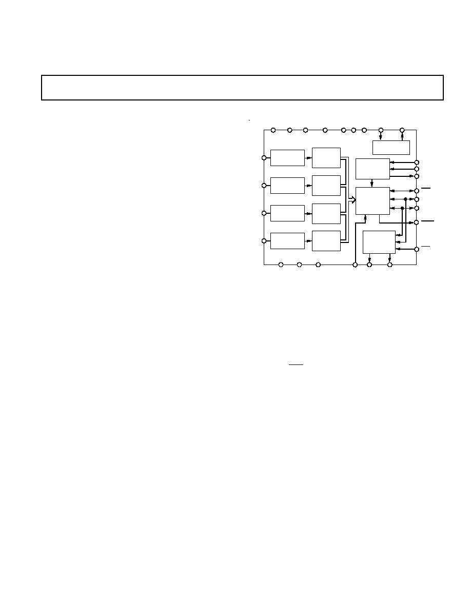
22-Bit Data Acquisition System
There are 22 bits of data corresponding to the analog input.
Two bits contain the channel address and 3 bits are the device
address. Thus, each channel in a 32-channel system would have
a discrete 5-bit address. The device also has a CASCOUT pin
and a CASCIN pin that allow simple networking of multiple
devices.
The on-chip control register is programmed using the SCLK,
SDATA and TFS pins. Three bits of the Control Register set
the digital filter cutoff frequency for the device. Selectable fre-
quencies are 584 Hz, 292 Hz, 146 Hz, 73 Hz and 36.5 Hz. A
further 2 bits appear as outputs D
OUT
1 and D
OUT
2 and can be
used for controlling calibration at the front end. The device is
available in a 44-pin PQFP (Plastic Quad Flatpack) and 44-pin
PLCC.
GENERAL DESCRIPTION
The AD7716 is a signal processing block for data acquisition
systems. It is capable of processing four channels with band-
widths of up to 584 Hz. Resolution is 22 bits and the usable
dynamic range varies from 111 dB with an input bandwidth of
36.5 Hz to 99 dB with an input bandwidth of 584 Hz.
The device consists of four separate A/D converter channels that
are implemented using sigma-delta technology. Sigma-delta
ADCs include on-chip digital filtering and, thus, the system
filtering requirements are eased.
Three address pins program the device address. This allows a
data acquisition system with up to 32 channels to be set up in a
simple fashion. The output word from the device contains 32
bits of data. One bit is determined by the state of the D
IN
1 in-
put and may be used, for example, in an ECG system with an
external pacemaker detect circuit to indicate that the output
word is invalid because of the presence of a pacemaker pulse.
FUNCTIONAL BLOCK DIAGRAM
CONTROL
LOGIC
OUTPUT
SHIFT
REGISTER
CONTROL
REGISTER
CLOCK
GENERATION
ANALOG
MODULATOR
LOW PASS
DIGITAL
FILTER
CLKOUT
CLKIN
V
REF
AGND
DGND
D
IN
1
D
OUT
1
D
OUT
2
MODE
CASCIN
CASCOUT
SDATA
SCLK
TFS
RFS
DRDY
A
IN
1
A
IN
2
A
IN
3
A
IN
4
AV
DD
DV
DD
AV
SS
A0 A1
A2
RESET
ANALOG
MODULATOR
LOW PASS
DIGITAL
FILTER
ANALOG
MODULATOR
LOW PASS
DIGITAL
FILTER
ANALOG
MODULATOR
LOW PASS
DIGITAL
FILTER
AD7716
FEATURES
22-Bit Sigma-Delta ADC
Dynamic Range of 105 dB (146 Hz Input)
0.003% Integral Nonlinearity
On-Chip Low-Pass Digital Filter
Cutoff Programmable from 584 Hz to 36.5 Hz
Linear Phase Response
Five Line Serial I/O
Twos Complement Coding
Easy Interface to DSPs and Microcomputers
Software Control of Filter Cutoff
5 V Supply
Low Power Operation: 50 mW
APPLICATIONS
Biomedical Data Acquisition
ECG Machines
EEG Machines
Process Control
High Accuracy Instrumentation
Seismic Systems
One Technology Way, P.O. Box 9106, Norwood, MA 02062-9106, U.S.A.
Tel: 617/329-4700
Fax: 617/326-8703
REV. A
Information furnished by Analog Devices is believed to be accurate and
reliable. However, no responsibility is assumed by Analog Devices for its
use, nor for any infringements of patents or other rights of third parties
which may result from its use. No license is granted by implication or
otherwise under any patent or patent rights of Analog Devices.

AD7716SPECIFICATIONS
1, 2
(f
CLKIN
= 8 MHz; MODE Pin Is High (Slave Mode Operation); AV
DD
= DV
DD
= +5 V
5%; AV
SS
= 5 V 5%; AGND = DGND = 0 V; V
REF
= 2.5 V; Filter Cutoff = 146 Hz; Noise Measurement Bandwidth = 146 Hz; A
IN
Source
Resistance = 750
2
with 1 nF to AGND at each A
IN
. T
A
= T
MIN
to T
MAX
, unless otherwise noted.)
Parameter
B Version
Units
Test Conditions/Comments
STATIC PERFORMANCE
Resolution
22
Bits
Integral Linearity Error
0.003
% FSR typ
Guaranteed No Missed Codes to 21 Bits
3
0.006
% FSR max
Gain Error
1
% FSR max
Gain Match Between Channels
0.5
% FSR max
Gain TC
30
µ
V/
°
C typ
Offset Error
0.2
% FSR max
Offset Match Between Channels
0.1
% FSR max
Offset TC
4
µ
V/
°
C typ
Noise
11
µ
V rms max
See Table I for Typical Noise Performance vs. Programmed
Cutoff Frequency
DYNAMIC PERFORMANCE
Sampling Rate
f
CLKIN
/14
570 kHz for f
CLKIN
= 8 MHz
Output Update Rate
f
CLKIN
/(14
256
2
N
)
N Is Decimal Equivalent of FC2, FC1, FC0 in Control Register
Filter Cutoff Frequency
f
CLKIN
/(3.81
14 256 2
N
)
Settling Time
(3 14 256 2
N
/f
CLKIN
)
Usable Dynamic Range
4
See Table I
Total Harmonic Distortion
90
dB typ
Input Frequency = 35 Hz
100
dB typ
A
IN
=
±
10 mV p-p
Absolute Group Delay
3
(3 14 256 2
N
)/2f
CLKIN
Differential Group Delay
3
10
ns typ
Channel-to-Channel Isolation
85
dB typ
Feedthrough from Any One Channel to the Other Three, with
35 Hz Full-Scale Sine Wave Applied to that Channel
ANALOG INPUT
Input Range
±
2.5
Volts
Input Capacitance
10
pF typ
Input Bias Current
1
nA typ
LOGIC INPUTS
V
INH
, Input High Voltage
2.4
V min
V
INL
, Input Low Voltage
0.8
V max
I
IN
, Input Current
SDATA, RFS
+10/-130
µ
A max
Internal 50 k
Pull-Up Resistors
TFS
+10/-650
µ
A max
Internal 10 k
Pull-Up Resistor
All Other Inputs
±
10
µ
A max
C
IN
, Input Capacitance
3
10
pF max
LOGIC OUTPUTS
V
OH
, Output High Voltage
2.4
V min
|I
OUT
|
40
µ
A
V
OL
, Output Low Voltage
0.4
V max
|I
OUT
|
1.6 mA
POWER SUPPLIES
Reference Input
2.4/2.6
V min/V max
AV
DD
4.75/5.25
V min/V max
DV
DD
4.75/5.25
V min/V max
AV
SS
4.75/5.25
V min/V max
I
DD
7.5
mA max
4.8 mA typ
I
SS
2.5
mA max
1.8 mA typ
Power Consumption
50
mW max
35 mW typ
Power Supply Rejection
5
70
dB typ
NOTES
1
Operating temperature ranges as follows : B Version; 40
°
C to +85
°
C.
2
The A
IN
pins present a very high impedance dynamic load which varies with clock frequency.
3
Guaranteed by design and characterization. Digital filter has linear phase.
4
Usable dynamic range is guaranteed by measuring noise and relating this to the full-scale input range.
5
100 mV p-p, 120 Hz sine wave applied to each supply.
Specifications subject to change without notice.
REV. A
2
REV. A
3
AD7716
Table I. Typical Usable Dynamic Range, RMS Noise and Filter Settling Time vs. Filter Cutoff Frequency
Programmed Cutoff
Output Update
Usable Dynamic
RMS Noise
Filter Settling Time to
Absolute Group
N
Frequency (Hz)
Rate (Hz)
Range (dB)
( V)
0.0007% FS (ms)
Delay (ms)
0
584
2232
99
21
1.35
0.675
1
292
1116
102
14
2.7
1.35
2
146
558
105
10
5.4
2.7
3
73
279
108
7
10.8
5.4
4
36.5
140
111
5
21.6
10.8
NOTE
Usable Dynamic Range is defined as the ratio of the rms full-scale reading (sine wave input) to the rms noise of the converter.
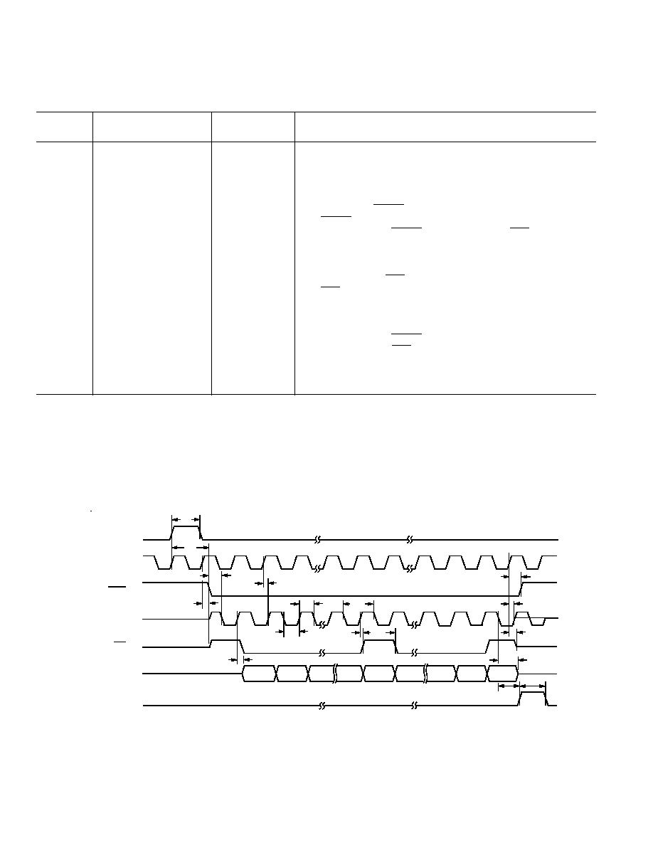
CONTROL REGISTER TIMING CHARACTERISTICS
1, 2
(AV
DD
= DV
DD
= +5 V
5%; AV
SS
= 5 V
5%; AGND =
DGND = 0 V; f
CLKIN
= 8 MHz; Input Levels: Logic 0 = 0 V, Logic 1 = DV
DD
; unless otherwise noted)
Limit at T
MIN
, T
MAX
Parameter
(B Version)
Units
Conditions/Comments
t
1
1/f
CLKIN
ns min
SCLK Period
t
2
77
ns min
SCLK Width
t
3
30
ns min
TFS
Setup Time
t
4
20
ns min
SDATA Setup Time
t
5
10
ns min
SDATA Hold Time
t
6
20
ns min
TFS
Hold Time
NOTES
1
Sample tested at +25
°
C to ensure compliance. All input signals are specified with tr = tf = 5 ns (10% to 90% of 5 V) and timed from a voltage level of 1.6 V.
2
See Figure 2.
3
CLKIN Duty Cycle range is 40% to 60%.
200
µ
A
I
OH
+2.1V
TO
OUTPUT
PIN
1.6mA
C
L
50pF
I
OL
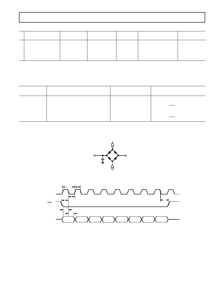
Figure 1. Load Circuit for Access Time and Bus Relinquish Time
DB4
(DB12)
DB3
(DB11)
DB2
(DB10)
DB1
(DB9)
DB0
(DB8)
DB5
(DB13)
DB6
(DB14)
DB7
(DB15)
t
2
SCLK (I)
SDATA (I)
TFS (I)
t
2
t
5
t
4
t
3
t
6
t
1
Figure 2. Control Register Timing Diagram
REV. A
AD7716
4
Limit at T
MIN
, T
MAX
Parameter
(B Version)
Units
Conditions/Comments
f
CLKIN
3, 4
400
kHz min
CLKIN Frequency
8
MHz max
t
r
5
40
ns max
Digital Output Rise Time. Typically 20 ns
t
f
5
40
ns max
Digital Output Fall Time. Typically 20 ns
t
7
1/f
CLKIN
ns min
CASCIN Pulse Width
t
8
1/f
CLKIN
ns min
CASCIN to DRDY Setup Time
t
9
1/2f
CLKIN
+ 30
ns max
DRDY
Low to SCLK Low Delay
t
10
50
ns max
CLKIN High to DRDY Low, SCLK Active, RFS Active
t
11
40
ns max
CLKIN High to SCLK High Delay
t
12
50
ns min
SCLK Width
t
13
1/f
CLKIN
ns
SCLK Period
t
14
40
ns max
SCLK High to RFS High Delay
t
15
1/f
CLKIN
ns
RFS
Pulse Width
t
16
6
45
ns max
SCLK High to SDATA Valid Delay
t
17
7
1/2f
CLKIN
+ 50
ns max
SCLK Low to SDATA High Impedance Delay
1/2f
CLKIN
+ 10
ns min
t
18
1/2f
CLKIN
+ 60
ns max
CLKIN High to DRDY High Delay
t
19
50
ns max
CLKIN High to RFS High Impedance, SCLK High Impedance
20
ns min
t
20
1/2f
CLKIN
+ 50
ns max
SCLK Low to CASCOUT High Delay
t
21
2/f
CLKIN
ns
CASCOUT Pulse Width
NOTES
1
Sample tested at +25
°
C to ensure compliance. All input signals are specified with tr = tf = 5 ns (10% to 90% of 5 V) and timed from a voltage level of 1.6 V.
2
See Figures 1 and 3.
3
CLKIN duty cycle range is 40% to 60%.
4
The AD7716 is production tested with f
CLKIN
at 8 MHz in the slave mode. It is guaranteed by characterization to operate at 400 kHz and 8 MHz in master mode.
5
Specified using 10% and 90% points on waveform of interest.
6
t
16
is measured with the load circuit of Figure 1 and defined as the time required for an output to cross 0.8 V or 2.4 V.
7
t
17
is derived from the measured time taken by the data outputs to change 0.5 V when loaded with the circuit of Figure 1. The measured number is then extrapolated
back to remove the effects of charging or discharging the 100 pF capacitor. This means that the time quoted in the timing characteristics is the true bus relinquish
time of the part and as such is independent of external bus loading capacitances.
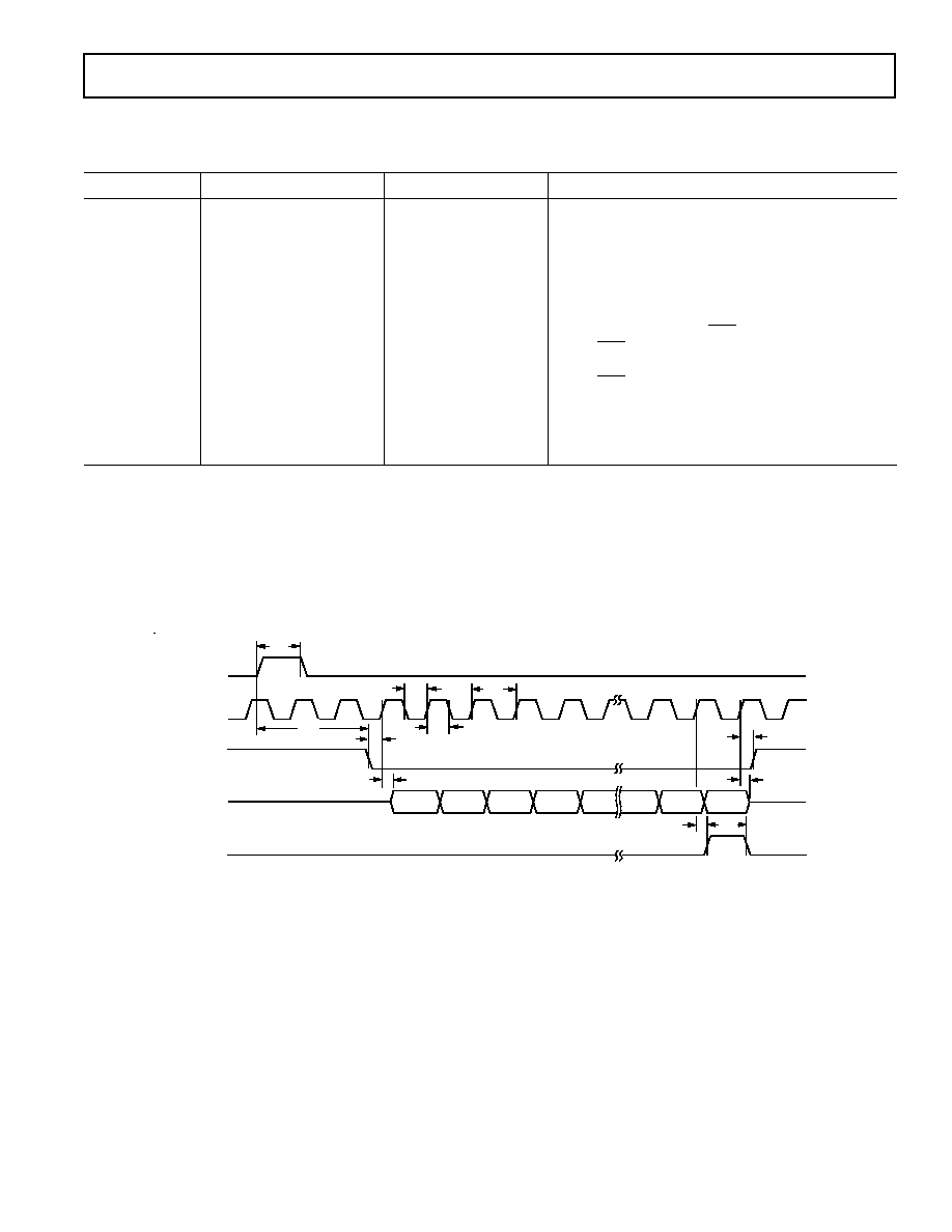
MASTER MODE TIMING CHARACTERISTICS
1, 2
(AV
DD
= DV
DD
= +5 V
5%; AV
SS
= 5 V
5%; AGND = DGND = 0 V;
f
CLKIN
= 8 MHz; Input Levels: Logic 0 = 0 V, Logic 1 = DV
DD
; unless otherwise noted)
Figure 3. Master Mode Timing Diagram
DB31
CH1
t
20
t
21
CASCIN (I)
SCLK (O)
RFS (O)
SDATA (O)
CASCOUT (O)
t
17
t
8
t
7
t
18
t
19
t
9
t
11
t
10
t
12
t
13
t
12
t
19
t
15
t
14
t
16
DB30
CH1
DB29
CH1
DB25
CH1
DB24
CH1
DB23
CH1
DB2
CH4
DB1
CH4
DB0
CH4
CLKIN (I)
DRDY (O)
REV. A
5
AD7716
SLAVE MODE TIMING CHARACTERISTICS
1, 2
(AV
DD
= DV
DD
= +5 V
5%; AV
SS
= 5 V
5%; AGND = DGND = 0 V;
f
CLKIN
= 8 MHz; Input Levels: Logic 0 = 0 V, Logic 1 = DV
DD
; unless otherwise noted)
Parameter
(B Version)
Units
Conditions/Comments
f
CLKIN
3, 4
400
kHz min
CLKIN Frequency
8
MHz max
t
r
5
40
ns max
Digital Output Rise Time. Typically 20 ns
t
f
5
40
ns max
Digital Output Fall Time. Typically 20 ns
t
23
1/f
CLKIN
ns min
CASCIN Pulse Width
t
24
50
ns min
SCLK Width
t
25
125
ns min
SCLK Period
t
26
1/f
CLKIN
+30
ns min
CASCIN High to RFS Setup Time
t
27
30
ns min
RFS
Low to SCLK High Setup Time
t
28
6
50
ns max
SCLK High to SDATA Valid Delay
t
29
50
ns min
RFS
Hold Time After SCLK High
t
30
7
50
ns max
SCLK High to SDATA High Impedance Delay
0
ns min
t
31
60
ns max
SCLK High to CASCOUT High Delay.
t
32
2/f
CLKIN
ns max
CASCOUT Pulse Width
NOTES
1
Sample tested at +25
°
C to ensure compliance. All input signals are specified with tr = tf = 5 ns (10% to 90% of 5 V) and timed from a voltage level of 1.6 V.
2
See Figures 1 and 4.
3
CLKIN duty cycle range is 40% to 60%.
4
The AD7716 is production tested with f
CLKIN
at 8 MHz in the slave mode. It is guaranteed by characterization to operate at 400 kHz.
5
Specified using 10% and 90% points on waveform of interest.
6
t
28
is measured with the load circuit of Figure 1 and defined as the time required for an output to cross 0.8 V or 2.4 V.
7
t
30
is derived from the measured time taken by the data outputs to change 0.5 V when loaded with the circuit of Figure 1. The measured number is then extrapolated
back to remove the effects of charging or discharging the 100 pF capacitor. This means that the time quoted in the timing characteristics is the true bus relinquish
time of the part and as such is independent of external bus loading capacitances.
Figure 4. Slave Mode Timing Diagram
t
31
CASCIN (I)
SDATA (O)
CASCOUT (O)
t
23
t
29
t
27
t
24
t
24
t
32
SCLK (I)
t
25
t
30
DB31
CH1
DB30
CH1
DB29
CH1
DB28
CH1
DB27
CH1
DB2
CH4
DB1
CH4
DB0
CH4
t
26
t
28
RFS (I)
REV. A
AD7716
6
ABSOLUTE MAXIMUM RATINGS
1
(T
A
= +25
°
C unless otherwise noted)
AV
DD
to AGND . . . . . . . . . . . . . . . . . . . . . . . . 0.3 V to +7 V
AV
SS
to AGND . . . . . . . . . . . . . . . . . . . . . . . +0.3 V to 7 V
AGND to DGND . . . . . . . . . . . . . . . . . . . . . 0.3 V to +0.3 V
AV
DD
to DV
DD
. . . . . . . . . . . . . . . . . . . . . . . 0.3 V to +0.3 V
Analog Inputs to AGND . . . . . . AV
SS
0.3 V to AV
DD
+ 0.3 V
V
REF
to AGND . . . . . . . . . . . . AV
SS
0.3 V to AV
DD
+ 0.3 V
Digital Inputs to DGND
2
. . . . . . . . . . 0.3 V to DV
DD
+ 0.3 V
Digital Outputs to DGND . . . . . . . . . . 0.3 V to DV
DD
+ 0.3 V
Operating Temperature Range
Commercial Plastic (B Versions) . . . . . . . . . . . 40
°
C to +85
°
C
Storage Temperature Range . . . . . . . . . . . . . 65
°
C to +150
°
C
PQFP Package, Power Dissipation . . . . . . . . . . . . . . . 450 mW
JA
Thermal Impedance . . . . . . . . . . . . . . . . . . . . . . 95
°
C/W
Lead Temperature, Soldering
Vapor Phase (60 sec) . . . . . . . . . . . . . . . . . . . . . . +215
°
C
Infrared (15 sec) . . . . . . . . . . . . . . . . . . . . . . . . . . +220
°
C
PLCC Package, Power Dissipation . . . . . . . . . . . . . . . 500 mW
JA
Thermal Impedance . . . . . . . . . . . . . . . . . . . . . . 55
°
C/W
Lead Temperature, Soldering
Vapor Phase (60 sec) . . . . . . . . . . . . . . . . . . . . . . +215
°
C
Infrared (15 sec) . . . . . . . . . . . . . . . . . . . . . . . . . . +220
°
C
NOTES
1
Stresses above those listed under "Absolute Maximum Ratings" may cause
permanent damage to the device. This is a stress rating only and functional
operation of the device at these or any other conditions above those listed in the
operational sections of this specification is not implied. Exposure to absolute
maximum rating conditions for extended periods may affect device reliability.
2
Transient currents of up to 100 mA will not cause SCR latch-up.
CAUTION
ESD (electrostatic discharge) sensitive device. Electrostatic charges as high as 4000 V readily
accumulate on the human body and test equipment and can discharge without detection.
Although these devices feature proprietary ESD protection circuitry, permanent damage may
occur on devices subjected to high energy electrostatic discharges. Therefore, proper ESD
precautions are recommended to avoid performance degradation or loss of functionality.
WARNING!
ESD SENSITIVE DEVICE
PQFP PINOUT
PLCC PINOUT
NC = NO CONNECT
MODE
NC
D
IN
1
NC
CASCIN
NC
DV
DD
NC
NC
NC
RFS
SCLK
D
OUT
1
DGND
NC
CLKIN
D
OUT
2
DGND
NC
A2
AGND
A
IN
3
AGND
AGND
A
IN
2
CLKOUT
SDATA
NC
AGND
A
IN
4
A0
A1
NC
V
REF
AV
SS
AGND
CASCOUT
AGND
AV
DD
A
IN
1
RESET
44
1
2
6
4
5
21
24
23
22
18
20
19
39
38
35
34
33
37
36
3
7
8
11
12
13
9
10
40
41
42
25
28
27
26
43
31
30
29
32
15
16
17
14
TOP VIEW
(Not to Scale)
AD7716
A2
AGND
TFS
DRDY
26 CASCOUT
NC = NO CONNECT
AGND 12
A2 13
AGND 14
A
IN
2 15
AGND 16
A
IN
3 17
AGND 18
A1 19
AGND 20
A
IN
4 21
A0 22
44 NC
43 CLKIN
42 NC
41 CLKOUT
40 D
OUT
2
38 DGND
37 NC
35 SDATA
34 NC
33 MODE
32 NC
31 NC
30 DV
DD
29 D
IN
1
28 NC
27 CASCIN
25 V
REF
24 AV
SS
23 AGND
NC 1
NC 2
D
OUT
1 3
DGND 4
NC 5
SCLK 7
RESET 8
AGND 9
AV
DD
10
A
IN
1 11
AD7716
TOP VIEW
(Not to Scale)
RFS 6
36 DRDY
39 TFS
ORDERING GUIDE
Temperature
Output Noise
Package
Model
Range
(Filter: 146 Hz)
Option
*
AD7716BP
40
°
C to +85
°
C
11
µ
V rms
P-44A
AD7716BS
40
°
C to +85
°
C
11
µ
V rms
S-44
*P = PLCC (Plastic Leaded Chip Carrier); S = PQFP (Plastic Quad Flatpack).

REV. A
7
AD7716
PIN DESCRIPTION
Pin
Description
AV
DD
Analog Positive Supply, +5 V Nominal. This supplies +ve power to the analog modulators. AV
DD
& DV
DD
must be tied together externally.
DV
DD
Digital Positive Supply, +5 V Nominal. This supplies +ve power to the digital filter and input/output registers.
AV
SS
Analog Negative Supply, 5 V nominal. This supplies ve power to the analog modulators.
RESET
A high pulse on this input pin synchronizes the sampling point on the four input channels. It can be used in a
multichannel system to ensure simultaneous sampling. This also resets the digital interface to a known state.
A0A2
The three address input pins, A0, A1 and A2 give the device a unique address. This information is contained in
the output data stream from the device.
CLKIN
Clock Input for External Clock.
CLKOUT
Clock Output which is used to generate an internal master clock by connecting a crystal between CLKOUT and
CLKIN. If an external clock is used then CLKOUT is not connected.
MODE
This digital input determines the device interface mode. If it is hardwired low, then the Master Mode interface is
enabled whereas if it is high, the Slave Mode interface is enabled.
CASCIN
This is an active-high, level-triggered digital input which is used to enable the output data stream. This input
may be used to cascade several devices in a multichannel system.
CASCOUT
Digital output which goes high at the end of a complete 4-channel data transfer. This can be connected to the
CASCIN of the next device in a multichannel system to ensure proper control of the data transfer.
RFS
Receive Frame Synchronization signal for the serial output data stream. This can be an input or output depending
on the interface mode.
SDATA
Serial Data Input/Output Pin.
SCLK
Serial Clock Input/Output. The SCLK pin is configured as an input or output, depending on the state of the
Mode pin.
DRDY
Data Ready Output. A falling edge indicates that a new word is available for transmission. It will return high
when 4, 32-bit words have been transmitted. It also goes high for one clock cycle, when a new word is being
loaded into the output register. Data should not be read during this period.
TFS
Transmit Frame Sync input for programming the on-chip Control Register.
D
IN
1
Digital Data Input. This is contained in the digital data stream sent from the device.
D
OUT
1, D
OUT
2
Digital Outputs. These two digital outputs can be programmed from the on-chip Control Register. They can
be used to control calibration signals at the front end.
V
REF
Reference Input, Nominally 2.5 V.
AGND
Analog Ground. Ground reference for analog circuitry.
DGND
Digital Ground. Ground return for digital circuitry.
A
IN
1A
IN
4
Analog Input Pins. The analog input range is
±
2.5 V.

REV. A
AD7716
8
OUTPUT UPDATE RATE
This is the rate at which the digital filter updates the output shift
register. It is a function of the master clock frequency and the
programmed filter cutoff frequency.
FILTER CUTOFF FREQUENCY
The digital filter of the AD7716 can be programmed, in binary
steps, to 5 discrete cutoff frequencies, ranging from 584 Hz to
36.5 Hz (for a CLKIN frequency of 8 MHz).
SETTLING TIME
This is the settling time of the on-chip digital filter, to 0.0007%
of FSR, in response to a full-scale step at the input of the ADC.
It is proportional to the master clock frequency and the filter
cutoff frequency.
USABLE DYNAMIC RANGE
The usable dynamic range is the ratio of the rms full-scale
reading (sine wave input) to the rms noise of the converter,
expressed in dBs. It determines the level to which it is possible
to resolve the input signal. For example, at a bandwidth of
146 Hz, the rms noise of the converter is 11
µ
V. The full-scale
rms is 1.77 volts. So, the usable dynamic range is 104 dB. Any
signal below this level will be indistinguishable from noise unless
extra post-filtering techniques are employed.
TOTAL HARMONIC DISTORTION
Total harmonic distortion (THD) is the ratio of the rms sum
of the harmonics to the fundamental. For the AD7716, it is
defined as:
THD (dB)
=
20 log
V
2
2
+
V
3
2
+
V
4
2
+
V
5
2
+
V
6
2
V
1
where V
1
is the rms amplitude of the fundamental and V
2
, V
3
,
V
4
, V
5
and V
6
are the rms amplitudes of the second through
sixth harmonics.
ABSOLUTE GROUP DELAY
Absolute group delay is the rate of change of phase versus fre-
quency, d
/df and is expressed in seconds. For the AD7716,
it is dependent on master clock frequency and filter cutoff
frequency.
DIFFERENTIAL GROUP DELAY
Differential group delay is the total variation in absolute group
delay in the specified bandwidth. Since the digital filter in the
AD7716 has perfectly linear phase, the differential group delay
is almost zero. This is important in many signal processing ap-
plications where excessive differential group delay can cause
phase distortion.
TERMINOLOGY
LINEARITY ERROR
This is the maximum deviation of any code from a straight line
passing through the endpoints of the transfer function. The
endpoints of the transfer function are zero scale (not to be con-
fused with Bipolar Zero), a point 0.5 LSB below the first code
transition (000 . . . 000 to 000 . . . 001) and full scale, a point
0.5 LSB above the last code transition (111 . . . 110 to
111 . . . 111). The error is expressed as a percentage of full
scale.
DIFFERENTIAL LINEARITY ERROR/NO MISSED CODES
This is the difference between any code's actual width and the
ideal (1 LSB) width. Differential Linearity Error is expressed in
LSBs. A differential linearity specification of
±
1 LSB or less
guarantees no missed codes to the full resolution of the device.
The AD7716 has no missed codes guaranteed to 21 bits with a
cutoff frequency of 146 Hz.
GAIN ERROR
Gain Error is the deviation of the last code transition
(111 . . . 110 to 111 . . . 1) from the ideal (V
REF
3/2 LSBs). It
is expressed as a percentage of full scale.
GAIN TC
This is the variation of gain error with temperature and is ex-
pressed in
µ
V/
°
C.
OFFSET ERROR
Offset Error is the deviation of the first code transition from the
ideal (V
REF
+ 0.5 LSB). It is expressed as a percentage of full
scale.
OFFSET TC
This is the variation of offset error with temperature and is ex-
pressed in
µ
V/
°
C.
NOISE
This is the converter rms noise expressed in
µ
V. Because of the
digital filtering in the sigma delta converter, the noise perfor-
mance is a function of the programmed filter cutoff.
SAMPLING RATE
This is the modulator sampling rate. For the AD7716, it is
f
CLKIN
/14.
REV. A
9
AD7716
GENERAL DESCRIPTION
The AD7716 is a 4-channel 22-bit A/D converter with on-chip
digital filtering, intended for the measurement of wide dynamic
range, low frequency signals such as those representing ECG,
EEG, chemical, physical or biological processes. It contains
four sigma delta ADCs, a clock oscillator and a serial communi-
cations port.
Each of the analog input signals to the AD7716 is continuously
sampled at a rate determined by the frequency of the master
clock, CLKIN. Four sigma-delta modulators convert the
sampled signals into digital pulse trains whose duty cycles con-
tain the digital information. These are followed by low-pass fil-
ters to process the output of the modulators and update the
output register at a maximum rate of 2.2 kHz. The output data
can be read from the serial port at any rate up to this.
THEORY OF OPERATION
The general block diagram of a delta-sigma ADC is shown in
Figure 5. It contains the following elements:
1. Continuously Sampling Integrator
2. A Differential Amplifier or Subtracter
3. A 1-Bit A/D Converter (Comparator)
4. A 1-Bit DAC
5. A Digital Low-Pass Filter
In operation, the sampled analog signal is fed to the subtracter,
along with the output of the 1-bit DAC. The filtered difference
signal is fed to the comparator, whose output samples the differ-
ence signal at a frequency many times that of the analog signal
frequency (oversampling).
Oversampling is fundamental to the operation of delta-sigma
ADCs. Using the quantization noise formula for an ADC:
SNR = (6.02
number of bits + 1.76) dB,
a 1-bit ADC or comparator yields an SNR of 7.78 dB.
When operating with a master clock of 8 MHz, the AD7716
samples the input signal at 570 kHz, which spreads the quanti-
zation noise from 0 kHz to 285 kHz. Since the specified analog
input bandwidth of the AD7716 is only 584 Hz maximum (it
can be programmed to be lower), the noise energy in this band-
width would be only 1/488 of the total quantization noise, as-
suming that the noise energy was spread evenly throughout the
spectrum. This very high sampling with respect to the input
bandwidth is known as oversampling, and the ratio of 488:1 is
called the oversampling ratio. The noise is reduced still further
by analog filtering in the modulator loop, which shapes the
quantization noise spectrum to move most of the noise energy to
frequencies above 584 Hz. The SNR performance in the 0 Hz
to 584 Hz range is conditioned to the 99 dB level in this fashion
(see Table I). As the programmed bandwidth is reduced, the
oversampling ratio increases and the usable dynamic range also
increases. Thus, for example, with a programmed bandwidth
of 73 Hz, the oversampling ratio is 3904:1, and the usable dy-
namic range is 108 dB which corresponds to greater than 17-bit
resolution.
The output of the comparator provides the digital input for the
1-bit DAC, so the system functions as a negative feedback loop
which minimizes the difference signal. The digital data that rep-
resents the analog input voltage is in the duty cycle of the pulse
train appearing at the output of the comparator. It can be re-
trieved as a parallel binary data word using a digital filter.
+V
REF
V
REF
INTEGRATOR
STROBED
COMPARATOR
CLOCK
C
TO
DIGITAL
FILTER
R
R
A
IN
1-BIT DAC
EN
Figure 5. First Order Modulator
Sigma-delta ADCs are generally described by the order of the
analog low-pass filter. A simple example of a first order sigma-
delta ADC is shown in Figure 5. This contains only a first-
order low-pass filter or integrator.
The AD7716 uses a second-order sigma-delta modulator and a
digital filter that provides a rolling average of the sampled out-
put. After power-up or if there is a step change in the input
voltage, there is a settling time before valid data is obtained.
DIGITAL FILTERING
The AD7716's digital filter behaves like an analog filter, with a
few minor differences.
First, since digital filtering occurs after the A-to-D conversion
process, it can remove noise injected during the conversion pro-
cess. Analog filtering cannot do this.
On the other hand, analog filtering can remove noise super-
imposed on the analog signal before it reaches the ADC. Digital
filtering cannot do this and noise peaks riding on signals near
full scale have the potential to saturate the analog modulator
and digital filter, even though the average value of the signal is
within limits. If noise signals cause the input signal to exceed
the specified range, consideration should be given to analog in-
put filtering, or to reducing the gain in the input channel to
bring the combination of signal and noise spike within the speci-
fied input range.
Filter Characteristics
The cutoff frequency of the digital filter is determined by bits
FC2, FC1 and FC0 in the control register (See Table IV). The
cutoff frequency of the filter is f
CLKIN
/(3.81 14 256 2N),
where N is the decimal equivalent of FC2, FC1, FC0. At the
maximum clock frequency of 8 MHz, with all 0s loaded to FC2,
FC1, FC0, the cutoff frequency of the filter is 584 Hz and the
data update rate is 2232 Hz.
Since the AD7716 contains low-pass filtering, there is a settling
time associated with step function inputs, and data will be in-
valid after a step change until the settling time has elapsed. The
REV. A
AD7716
10
relationship between input bandwidth and settling is given in
Table I. Because of this settling time, most sigma delta ADCs
are unsuitable for high speed multiplexing, where channels are
switched and converted sequentially at high rates, as switching
between channels can cause a step change in the input. How-
ever, the AD7716 is a sigma-delta solution to multichannel ap-
plications, since it can process four channels simultaneously. In
addition, it is easy to cascade several devices in order to increase
the number of channels being processed.
Figure 6. Frequency Response of AD7716 Filter
Figure 6 shows the filter frequency response for a cutoff fre-
quency of 73 Hz. This is a (sinx/x)
3
response (also called sinc
3
)
that provides greater than 100 dB rejection at the notch fre-
quencies. The relationship between the programmed cutoff
frequency and the first notch is constant (f
NOTCH
= 3.81
f
CUTOFF
). The first notch frequency is also the output data rate.
The settling time to a full-scale step input is four times the out-
put data period. Programming a different cutoff frequency via
FC0FC2 does not alter the profile of the filter response, it sim-
ply changes the frequency of the notches.
In Figure 6, the first notch is at 278 Hz. This is also the output
data rate. Settling time to a full-scale step input is 10.8 ms.
The digital filter can be defined by the following equations.
H ( z )
=
1
N
×
1 Z
N
1 Z
1
3
H ( f )
=
sin
f / f
S
)
f / f
S
)
3
where N = Ratio of Modulator Sampling Frequency to Output
Rate
and
f
S
= Output Rate.
Post Filtering
In the AD7716, the on-chip modulator provides the digital filter
with samples at a rate of 570 kHz. The filter decimates these
samples to provide data at an output rate which corresponds to
the programmed first notch frequency of the filter.
If the user wants to reduce the output noise from the device for
bandwidths less than 36.5 Hz, then it is possible to employ extra
filtering after the AD7716. This extra digital filtering is called
post filtering. If a straight averaging filter is used, for example, a
reduction in bandwidth by a factor of 2 results in
2
reduction
in the rms noise. This additional filtering will also result in a
longer settling time.
Antialias Considerations
The digital filter does not provide any rejection at integer mul-
tiples of the modulator sampling frequency (n 570 kHz,
where n = 1, 2, 3, . . .). This means that there are frequency
bands,
±
f
3dB
wide (f
3dB
is the cutoff frequency selected by FC0
to FC2) where noise passes unattenuated to the output. How-
ever, due to the AD7716's high oversampling ratio, these bands
occupy only a small fraction of the spectrum and most broad-
band noise is filtered.
In spectral analysis applications, it is important to note that at-
tenuation at half the output update rate is 16 dB. Extra front-
end filtering or post filtering may be required to keep aliases in
this frequency band at an acceptable level.
USING THE AD7716
SYSTEM DESIGN CONSIDERATIONS
The AD7716 operates differently from successive approxima-
tion ADCs or other integrating ADCs. Since it samples the sig-
nal continuously, like a tracking ADC, there is no need for a
start convert command. The output register is updated at a rate
dependent on the programmed cutoff frequency, and the output
can be read at any time.
Input Signal Conditioning
The input range for the AD7716 is
±
V
REF
, where V
REF
= 2.5 V
±
10%. Other input ranges can be accommodated by input sig-
nal conditioning. This may take the form of gain to increase a
smaller signal range, or passive attenuation to reduce a larger in-
put voltage range.
240
1668
73
0
0
180
220
200
120
160
140
100
80
60
20
40
1390
1112
834
556
278
FREQUENCY Hz
GAIN d
B
REV. A
11
AD7716
Source Resistance
If passive attenuators are used in front of the AD7716, care
must be taken to ensure that the source impedance is suffi-
ciently low. The dc input resistance for the AD7716 is greater
than 1 G
. In parallel with this there is a small sampling ca-
pacitor. The dynamic load presented by this varies with the
clock frequency. The modulator sampling rate determines the
amount of time available for the sampling capacitor to be
charged. Any extra external impedances result in a longer over-
all charge time resulting in extra gain errors on the analog input.
The AD7716 has a quite large gain error (1% FSR) due to the
fact that there is no on-chip calibration. Thus, even an extra
10 k
source resistance and 50 pF source capacitance will have
no significant effect on this.
Active signal conditioning circuits such as op amps generally do
not suffer from problems of high source impedance. Their
open-loop output resistance is normally only tens of ohms and,
in any case, most modern general purpose op amps have
sufficiently fast closed-loop settling time for this not to be a
problem.
Accuracy
Sigma-delta ADCs, like VFCs and other integrating ADCs, do
not contain any source of nonmonotonicity and inherently offer
no missing codes performance.
The AD7716 achieves excellent linearity by the use of high
quality, on-chip silicon dioxide capacitors, which have a very
low capacitance/voltage coefficient.
Drift Considerations
The AD7716 uses autozeroing techniques to minimize input
offset drift. Charge injection in the analog switches and leakage
currents at the sampling node are the primary sources of offset
voltage drift in the converter. Figure 7 indicates the typical off-
set due to temperature changes. Drift is relatively flat up to
85
°
C. Above this temperature, leakage current becomes the
main source of offset drift. Since leakage current doubles ap-
proximately every 10
°
C, the offset drifts accordingly. The value
of the voltage on the sample capacitor is updated at a rate deter-
mined by the master clock, therefore the amount of offset drift
which occurs will be proportional to the elapsed time between
samples.
Gain drift within the converter depends mainly upon the tem-
perature tracking of the internal capacitors. It is not affected by
leakage currents.
Figure 7. Typical Offset Drift
Voltage Reference
The voltage applied to the V
REF
pin defines the analog input
range. The specified reference voltage is 2.5 V
±
10%.
The reference input presents exactly the same dynamic load as
the analog input, but in the case of the reference input, source
resistance and long settling time introduce gain errors rather
than offset errors. Most precision references however have suffi-
ciently low output impedance and wide enough bandwidth to
settle to the required accuracy in the time allowed by the
AD7716.
The reference should be chosen to have minimal noise in the
programmed passband. Recommended references are the
AD780 or the REF43 from Analog Devices. These low noise
references have typical noise spectral densities of 100 nV/
Hz
at
600 Hz. This corresponds to an rms noise of 2.5
µ
V in this
band and is more than adequate for the AD7716.
Clock Generation
The device operates from a master clock which must be pro-
vided either from a crystal source or an external clock source. If
a crystal is used, it must be connected across the CLKIN and
CLKOUT pins. Typical loading capacitors of 15 pF are re-
quired on CLKIN, CLKOUT. The crystal manufacturers data
should be consulted for more information. An external clock
can also be used to drive the CLKIN input directly with a
CMOS compatible clock. In this case, CLKOUT is left uncon-
nected. The nominal clock frequency for the device is 8 MHz.
0.125
0.625
20
90
0.25
0.500
30
0.375
70
80
60
50
40
TEMPERATURE
°
C
OFFSET VOLTAGE mV

REV. A
AD7716
12
Control register bit, DB15 (A3), acts as an extra address bit
which must always be set to 1 to enable programming of the
AD7716. If it is set to 0, then the programmed word is ignored.
This allows the user to bypass the AD7716 control register and
use the serial stream from the DSP or microcomputer to pro-
gram other serial peripheral devices.
When a valid word has been received, the device interrogates
the M0 bit. If this is 0, then the digital filter cutoff frequencies
are programmed to the appropriate value if the device address
pins correspond to the A2, A1, A0 bits in the control register. If
the device address pins do not correspond to the A2, A1, A0
bits then the FC2, FC1, FC0 bits are ignored. If M0 is 1, then
the digital filter cutoff frequencies are programmed to the FC2,
FC1, FC0 value irrespective of the address bits. In a multi-
channel system this allows the user to either program all
AD7716s to have the same cutoff frequency or else to give each
device a separate cutoff frequency.
Control register bits FC2, FC1, FC0 program the digital filter
cutoff frequency, see Table VI.
Control register bits D2, D1 control the digital output pins D2
and D1. These are programmed in the same way as FC2, FC1,
FC0.
CONTROL REGISTER DESCRIPTION
The 16-bit control register is programmed in two 8-bit bytes;
the low byte is programmed first and the high byte second. The
loading format is LSB first (DB0 for the Least Significant Byte;
DB8 for the Most Significant Byte). Three control lines are
used: TFS, SCLK and SDATA. On initial application of
power to the AD7716, the control register will come up in an
undetermined state. Programming the control register requires
an SCLK input, a TFS input and an SDATA input. The
MODE pin on the device determines whether it is in the master
interface mode or the slave interface mode. In either mode, a
falling edge on TFS causes the part to relinquish control of the
SDATA and SCLK lines. When TFS goes low, data on the
SDATA line is clocked into the control register on each suc-
ceeding falling edge of SCLK. When 8 bits have been clocked
in, the transfer automatically stops. Only when another negative
going edge is detected on TFS will new information be written
into the control register. The control register programming
model is shown in Table II. Bits DB8 and DB0 allow the con-
trol register to identify whether the MS Byte or the LS Byte has
been programmed. Only when DB8 is a 1 and DB0 is a 0 will
the register recognize that a complete valid word has been
programmed.
Table II. Control Register Programming Model
Most Significant Byte
Least Significant Byte
DB15
DB14
DB13
DB12
DB11
DB10
DB9
DB8
DB7
DB6
DB5
DB4
DB3
DB2
DB1
DB0
A3
A2
A1
A0
M0
FC2
FC1
1
FC0
DOUT2 DOUT1
X
X
X
X
0
Table III. M0 Truth Table
M0
Programming Mode
0
A2, A1, A0 determine which device is addressed and
programmed with cutoff frequency and digital output.
1
A2, A1, A0 ignored. All devices are addressed and
programmed with common cutoff frequency and digital
output.
Table IV. Cutoff Frequency Truth Table
FC2
FC1
FC0
Cutoff Frequency (Hz)
0
0
0
584
0
0
1
292
0
1
0
146
0
1
1
73
1
0
0
36.6

REV. A
13
AD7716
RESET
The AD7716 has a hardware reset which can be used to synchro-
nize many devices. When the RESET pin goes low after being
high for at least four CLKIN cycles, the modulator sampling
points and digital filter starting points are all synchronized. This
synchronizes all devices which receive the RESET pulse and
gives simultaneous sampling of all channels. It does not affect
the control register but restarts the interface. Also, it is necessary
to wait the requisite settling time after applying Reset to get valid
data from the device.
CASCADING DEVICES
The AD7716 provides a facility for connecting multiple devices
in series. The CASCIN and CASCOUT pins allow this. Con-
necting CASCOUT to CASCIN of the succeeding device means
that the SDATA output of the second device will be disabled un-
til the output register of the first device is empty.
In the case of the first device in the system, it is possible to drive
CASCIN from CASCOUT of the last device or, alternatively,
invert DRDY to drive it. If CASCIN is driven by CASCOUT,
then a reset must be applied after every write to the control
register. This also applies in single device systems that use
CASCOUT to drive CASCIN
DATA OUTPUT INTERFACE MODES
When the control register has been programmed, the device be-
gins conversion. There is an initial delay to allow the digital fil-
ters to settle. As already stated, these filters are Sinc
3
,
and so the
filter output update rate is directly related to the programmed
cutoff frequency. The ratio between these is 3.81. So, for a filter
cutoff frequency of 584 Hz, the output update is 2.22 kHz. The
falling edge of the DRDY output indicates that the output shift
register has been updated. There are two interface modes. One
is the master mode, where the AD7716 is the master in the sys-
tem and the processor to which it is communicating is the slave.
The other mode is the slave mode, where the AD7716 is the
slave and the processor is the system master. In both of these
modes the data output stream contains 4
32 bits, correspond-
ing to the four input channels. The output data format is given
in Table V. The conversion result DB21DB0 occupies location
DB31DB10 of the output register. DB21 is the MSB and is
transmitted first as shown in the timing diagrams. The channel
address is given by CA0 and CA1 which occupy DB9 and DB8
of the output register. The channel address format is given in
Table VI.
Table V. Output Data Word Format
DB31 . . . DB10
DB9
DB8
DB7
DB6 DB5
DB4
DB3
DB2
DB1
DB0
DB21 . . . DB0
CA0
CA1
A0
A1
A2
D
IN
1
OVFL
X
X
X
Conversion Result
Channel Address
Device Address
Pace Detect
Overflow
Indeterminate
Master Mode Interface
The device may be placed in the Master Mode by tying the
MODE pin low. In this mode, data is clocked out of the
AD7716 by an internally generated serial clock and frame syn-
chronization pulse. Two signals initiate the transfer. These are
the input CASCIN and the internally generated DRDY signal.
When a high level is detected on CASCIN, the device checks
the state of DRDY. Note, that on initial power-up or after a re-
set has been applied, the CASCIN input is not necessary on de-
vice 000 for the first data transfer but is required thereafter. If
DRDY
is low, then the 3-state output, RFS goes high on the
next rising edge of CLKIN and stays high for one CLKIN cycle
before going low again. The 3-state SCLK output is also acti-
vated on the same rising edge. As RFS goes low, DB31 is
clocked out on the rising edge of SCLK and is valid on the fall-
ing edge of SCLK. Data is transmitted in 8-bit bytes. For each
A
IN
, there are 4, 8-bit bytes and 4 RFS pulses. When DB0 of
A
IN
4 has been clocked out, SCLK goes back into 3-state and
the CASCOUT output goes high for one master clock cycle.
DRDY
also goes high at this point. Successive devices can be
networked together by tying the CASCOUT of one device to
the CASCIN on the next one.
Note that on device 0 (A2, A1, A0 tied low), the CASCIN input
should be driven by the inverse of the DRDY output. This is
shown in the interface diagram of Figure 8.
The Master Mode interface is very suitable for loading data into
a serial-to-parallel shift register or for DSPs which can accept a
continuous stream of 8-bit bytes.
Slave Mode Interface
The device may be placed in the slave interface mode by tying
the MODE pin high. In this mode, the master processor con-
trols the transfer of data from the signal processing block. It
starts the transfer by sending a frame synchronizations pulse and
serial clock to the AD7716. This could be in response to an in-
terrupt generated by the DRDY output on the AD7716. If the
device has detected a high level on CASCIN or is device 000 on
its first transfer, it starts to send out data on the next rising edge
of SCLK. This data is then valid on the falling edge of SCLK.
When all the data bits have been clocked out, the CASCOUT
pin goes high for one CLKIN cycle and DRDY also goes high.
The slave mode interface is suited to both microcomputers like
the 8051 and 68HC11 and also DSPs like the TMS320C25,
ADSP-2101 family and the DSP56000 family.
Table VI. Channel Address Format
Channel
CA1 (DB8)
CA0 (DB9)
A
IN
1
0
0
A
IN
2
0
1
A
IN
3
1
0
A
IN
4
1
1
REV. A
AD7716
14
MICROPROCESSOR INTERFACING
Interfacing the AD7716 to the ADSP-2100 Family
The ADSP-2100 family of microcomputers from Analog De-
vices are high speed, high performance digital signal processors.
Many members of the family have serial ports (known as
SPORTs) which are compatible with the AD7716. These in-
clude the ADSP-2101, ADSP-2105, ADSP-2111 and ADSP-
2115. Full details of these are available in the ADSP-2100
Family User's Manual available from Analog Devices.
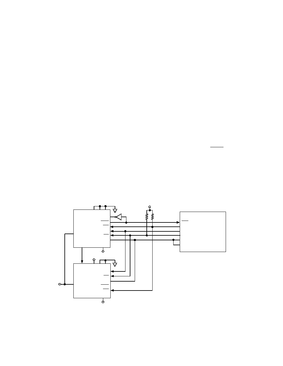
Figure 8 shows the hardware interface between two AD7716s
and SPORT 0 of the ADSP-2101 DSP. This yields a very effi-
cient 8-channel data acquisition system. The AD7716 is set up
for slave interface mode by tying the MODE pin high. This
means that the ADSP-2101 is the master in the system and sup-
plies the necessary frame synchronization and SCLK Signals to
the AD7716s when writing to and reading from the device.
On power up, the user should write to the AD7716 control reg-
ister in order to set the filter cutoff frequencies. The appropri-
ate SPORT 0 Control Register (0
3FF6) setting is "7EC7."
This sets the transmit section for alternate inverted framing with
a word length of 8 bits. Two 8-bit words should then be written
to each AD7716 to program the filter cutoff frequencies. The
control register programming model is given in Table II. Note
that the LSB (DB0) must be loaded first as in the timing dia-
gram of Figure 2.
When the write operation is complete, a reset pulse should be
applied to both devices. This ensures that the sampling and in-
terface timing of the device are synchronized. The reset can be
under DSP control, in which case a flag output could be used.
After reset, the processor should jump to the read routine. For
this read routine, there are several registers that need to be set.
The SPORT0 Control Register setting is "7FCF." This sets the
receive section for internal SCLK, continuous receive with al-
ternate inverted framing.
The SPORT0 SCLKDIV Register (0 3FF5) determines the
SCLK frequency from the ADSP-2101. With "0000" loaded,
the SCLK output is at its maximum (1/2 the master clock of
12.5 MHz).
In normal operation, a SPORT generates an interrupt when it
has received a data word. Autobuffering provides a mechanism
for receiving or transmitting an entire block of serial data before
an interrupt is generated. Service routines can operate on the
entire block of data, rather than on a single word, reducing over-
head significantly. This is ideal for use with a device like the
AD7716 where there is a requirement to read many bits of data
(256 in this case) for each sampling instant. The SPORT0
Autobuffer Control Register (0 3FF3) is loaded with "0001"
to enable the Receive Autobuffering.
The SPORT0 RFSDIV Register (0 3FF4) should be set to
the minimum value of "000F." Finally the IRQ2 interrupt
should be enabled.
The DSP will now wait for an interrupt from the AD7716. This
interrupt is generated by the AD7716 DRDY line going low. If
the interrupt service routine is set for autobuffered mode with a
length of 16 (16-bit) words, then the DSP will read in the 256
bits from the two AD7716s in one continuous stream and then
stop. The data from the two devices will be contained in the
designated data memory area and the DSP can now go and op-
erate on this as is necessary. Note that, because of the ADSP-
2101 framing, a one-bit shift left will be necessary on the data in
memory. For 16 data words, this will require 22 instruction
cycles.
ADSP-2101
CASCIN
A0 A1 A2
RESET
CASCOUT
MODE
TFS
SDATA
RFS
SCLK
AD7716 #1
CASCIN
A0 A1 A2
RESET
SDATA
SCLK
AD7716 #2
RESET
CONTROL
+5V
+5V
SCLK
TFS
DT
DR
IRQ2
(VE EDGE TRIGGERED)
RFS
DRDY
TFS
RFS
DRDY
CASCOUT
MODE
+5V
4.7k
4.7k
+5V
Figure 8. 8-Channel Data Acquisition System Using the ADSP-2101 Digital Signal Processor
REV. A
15
AD7716
The optimum setup for reading all four channels of the AD7716
into the DSP56001 is six 24-bit reads. This will provide 144 clock
edges to shift out the 128 bits of data in the AD7716 output shift
register. The first clock applied to the AD7716 will clock out
DB21 of A
IN
1. DRDY from the AD7716 can be used as an
interrupt input to the DSP56001 to control the data transfer.
Either IRQA or IRQB of the DSP56001 can be used to detect the
interrupt.
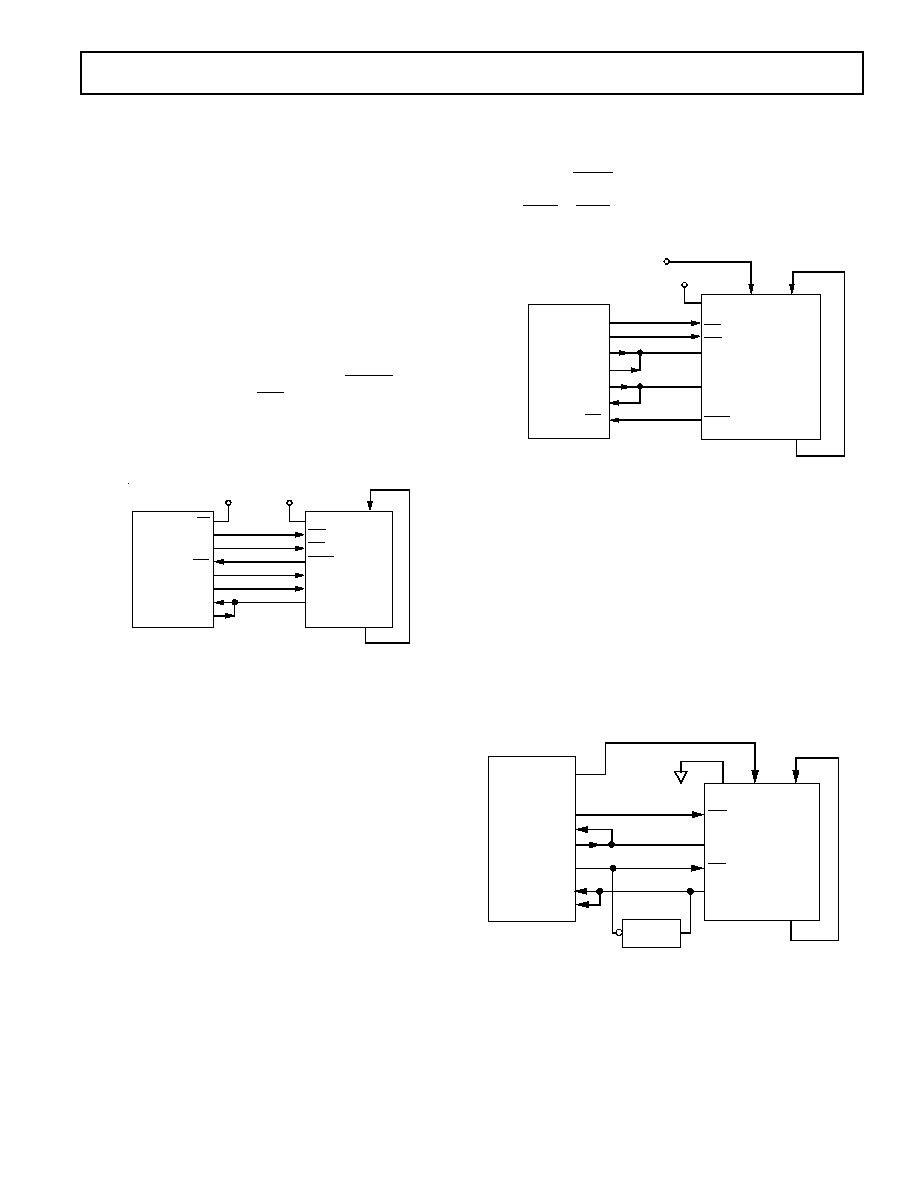
DSP56001
+5V
AD7716
CASCOUT
CASCIN
RESET
RESET
CONTROL
SC2
SC1
SCK
SC0
STD
SRD
IRQ
MODE
TFS
RFS
SCLK
SDATA
DRDY
Figure 10. DSP56001 Interface
TMS320C25 Interface
Figure 11 shows the AD7716 interfaced to the TMS320C25
DSP using the master mode interface. For initial programming
of the AD7716 control register, the external gated clock is re-
quired. FSX going low enables this. When the two 8-bit bytes
have been sent to the AD7716, the FSX should go permanently
high. The external gated clock will now be disabled and the
AD7716 will take control of the SDATA line. It will begin
transmitting data as soon as it becomes available. It also pro-
vides the clock and frame synchronization signals required by
the DSP.
Reset for the AD7716 is provided by one of the DSP flag
outputs.
FLAG
OUTPUT
FSR
DR
DT
FSX
CLKR
CLKX
MODE
RFS
RESET
CASCIN
AD7716
CASCOUT
TMS320C25
GATED
CLOCK
EN
RESET CONTROL
SDATA
TFS
SCLK
Figure 11. TMS320C25 to AD7716 Interface
When the AD7716 is programmed for the maximum cutoff fre-
quency of 584 Hz, the output data rate is 2.25 kHz. This
means that there is 440
µ
s available to read the data and do the
necessary number crunching before the next sample must be
read. Assuming that the ADSP-2101 is running from a master
clock of 12.5 MHz means that the maximum SCLK available is
6.25 MHz (1/2 the master clock frequency). It will then take 40
µ
s to transfer the 256 bits of data from the ADC to the DSP.
This leaves 400
µ
s for number crunching in the DSP. If the
programmed cutoff frequency is lower then this allows even
more time to the DSP.
MC68HC11 Interface
The MC68HC11 microcomputer can be interfaced to the
AD7716 using the slave mode interface. Figure 9 shows a typi-
cal setup. The MODE pin on the AD7716 is tied high for slave
mode operation. The SPI port of the MC68HC11 is used. The
microcomputer is in its single chip mode. DRDY from the
AD7716 is connected to the IRQ input of the MC68HC11.
MISO and MOSI on the MC68HC11 should be configured for
wired-or operation. Depending on the interface configuration,
it may be necessary to provide bidirectional buffers between
these lines.
PC0
PC1
PC2
PC3
SCK
MISO
MOSI
SS
MC68HC11
MODE
RFS
TFS
DRDY
RESET
SCLK
SDATA
AD7716
+5V
+5V
CASCOUT
CASCIN
PC0
PC1
IRQ
PC2
SCK
MISO
MOSI
SS
MC68HC11
MODE
RFS
TFS
DRDY
RESET
SCLK
SDATA
AD7716
+5V
+5V
CASCOUT
CASCIN
Figure 9. MC68HC11 to AD7716 Interface
The MC68HC11 is configured in the master mode with its
CPOL bit set to a logic zero and its CPHA bit set to a logic one.
With an 8 MHz CLKIN input on the AD7716, the device will
operate with all four serial clock rates of the MC68HC11.
Sixteen, 8-bit read operations are necessary to read the 128 bits
from the AD7716 output register. An extra read is necessary to
reset the output register. This means a total of 17 read opera-
tions are needed from the MC68HC11.
DSP56001 Interface
Figure 10 shows an interface to the DSP56001 digital signal
processor. The AD7716 is set up for the slave interface mode.
The DSP56001 is set up for asynchronous operation with gated
clock and normal framing. Data must be written to the
AD7716 control register in two 8-bit bytes. The first byte is
written to the DSP56001 SSI transmit data register (TX) and
this is automatically transferred to the transmit shift register
when the frame sync occurs. Data is shifted out to the STD pin
by the internal bit clock (SCK) when the associated frame sync
output is asserted.
REV. A
AD7716
16
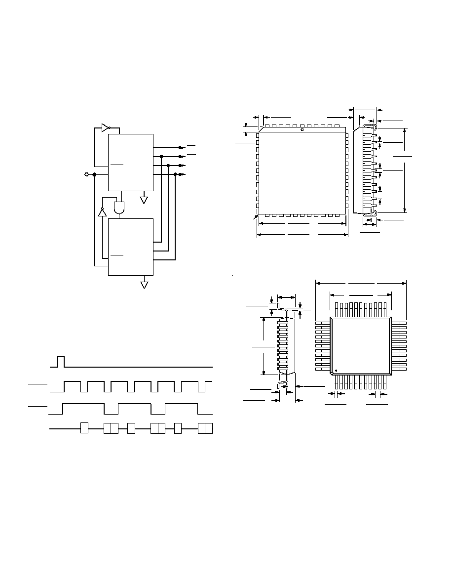
Multibandwidth System
Some applications may require multiple AD7716's with differ-
ent bandwidths programmed to each device. The best way to
accomplish this is shown in Figure 12. The master mode inter-
face is used for this example but the slave mode may also be
used. The example shows an 8-channel system with Device #0
in the system programmed for a 292 Hz cutoff frequency and
Device #1 programmed for a 146 Hz cutoff frequency.
CASCIN
DRDY
RESET
CASCOUT
MODE
#0
(292 Hz)
CASCIN
DRDY
RESET
MODE
#1
(146 Hz)
RESET
TFS
RFS
SCLK
SDATA
Figure 12. Multibandwidth System
The resultant output signals are also shown. Since Device #0
has a higher bandwidth it will also have a higher update rate.
The receiving processor will be getting samples from this device
at twice the rate of Device #1.
#0
#0 #1
#0
#0 #1
#0
#0 #1
RESET
DRDY #0
DRDY #1
SDATA
Figure 13. Output Signals for Figure 12
OUTLINE DIMENSIONS
Dimensions shown in inches and (mm).
44-Lead PLCC
(P-44A)
0.032 (0.81)
0.026 (0.66)
0.021 (0.53)
0.013 (0.33)
0.056 (1.42)
0.042 (1.07)
0.025 (0.63)
0.015 (0.38)
0.180 (4.57)
0.165 (4.19)
0.63 (16.00)
0.59 (14.99)
0.110 (2.79)
0.085 (2.16)
0.040 (1.01)
0.025 (0.64)
0.050
(1.27)
BSC
0.656 (16.66)
0.650 (16.51)
SQ
0.695 (17.65)
0.685 (17.40)
SQ
0.048 (1.21)
0.042 (1.07)
0.048 (1.21)
0.042 (1.07)
40
6
TOP VIEW
39
29
18
17
PIN 1
IDENTIFIER
7
28
0.020
(0.50)
R
44-Lead Plastic Quad Flatpack
(S-44)
0.083 (2.11)
0.077 (1.96)
0.016 (0.41)
0.012 (0.30)
0.033 (0.84)
0.029 (0.74)
1
44
34
33
23
22
12
11
TOP VIEW
PIN 1
0.398 (10.11)
0.390 (9.91)
0.557 (14.148)
0.537 (13.640)
0.096 (2.44)
MAX
0.037 (0.94)
0.025 (0.64)
0.398 (10.11)
0.390 (9.91)
0.040 (1.02)
0.032 (0.81)
0.040 (1.02)
0.032 (0.81)
8
°
0.8
°
PRINTED IN U.S.A.
C1920a211/95