Äîêóìåíòàöèÿ è îïèñàíèÿ www.docs.chipfind.ru
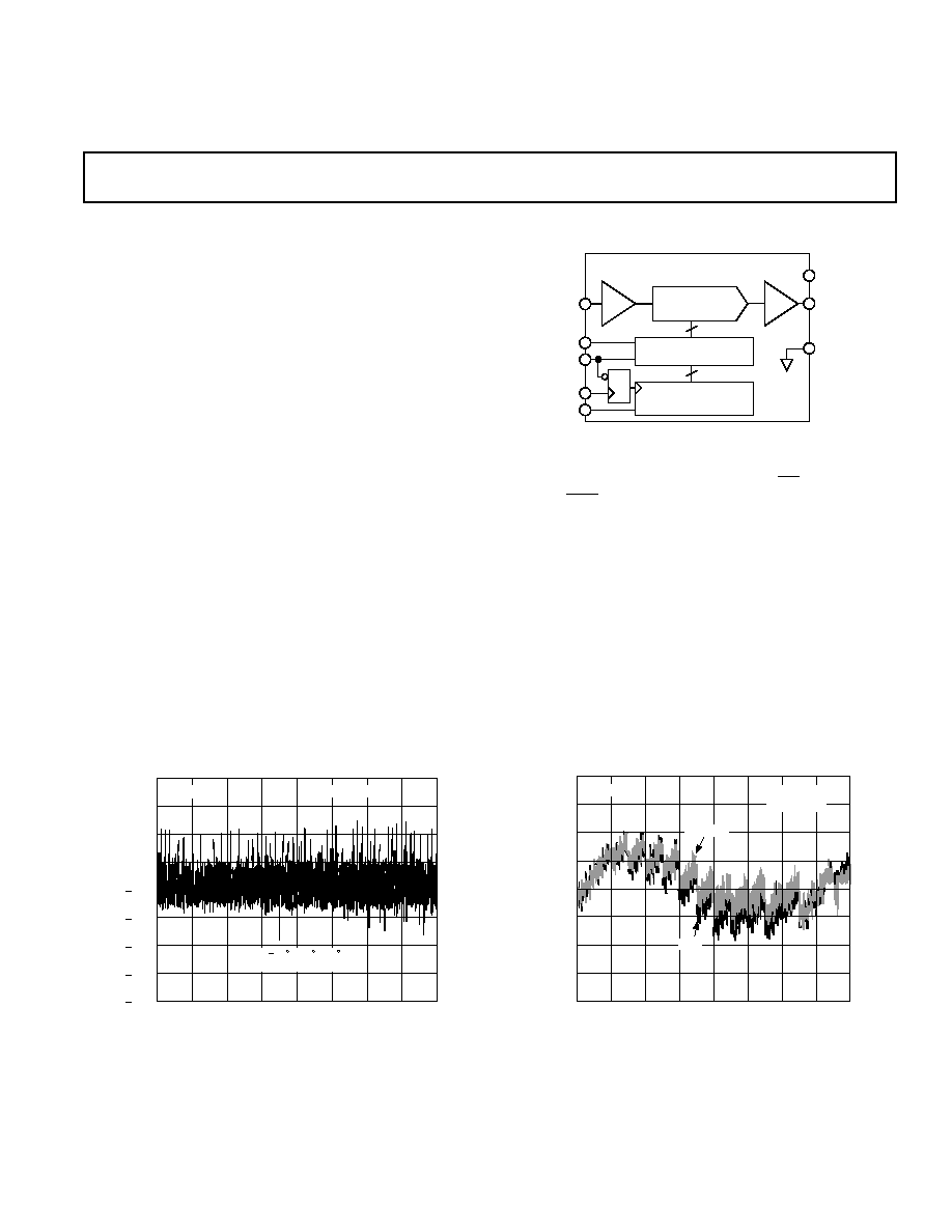
FUNCTIONAL DIAGRAM
REF
12-BIT DAC
DAC REGISTER
SERIAL REGISTER
12
CLR
CLK
SDI
V
DD
V
OUT
GND
12
EN
LD
AD7390
REV. 0
Information furnished by Analog Devices is believed to be accurate and
reliable. However, no responsibility is assumed by Analog Devices for its
use, nor for any infringements of patents or other rights of third parties
which may result from its use. No license is granted by implication or
otherwise under any patent or patent rights of Analog Devices.
a
+3 Volt Serial-Input
Micropower 10-Bit & 12-Bit DACs
FEATURES
Micropower--100 A
Single-Supply-- 2.7 to 5.5 V Operation
Compact 1.75 mm Height SO-8 Package
& 1.1 mm Height TSSOP-8
AD7390--12-Bit Resolution
AD7391--10-Bit Resolution
SPI & QSPI Serial Interface Compatible with Schmitt
Trigger Inputs
APPLICATIONS
Automotive 0.5 V to 4.5 V Output Span Voltage
Portable Communications
Digitally Controlled Calibration
GENERAL DESCRIPTION
The AD7390/AD7391 family of 10-bit & 12-bit voltage-output
digital-to-analog converters is designed to operate from a single
3 V supply. Built using a CBCMOS process, these monolithic
DACs offer the user low cost, and ease-of-use in single-supply
3 V systems. Operation is guaranteed over the supply voltage
range of 2.7 V to 5.5 V consuming less than 100
µ
A making
this device ideal for battery operated applications.
The full-scale voltage output is determined by the external ref-
erence input voltage applied. The rail-to-rail REF
IN
to DAC
OUT
allows for a full-scale voltage set equal to the positive supply
V
DD
or any value in between.
A doubled-buffered serial-data interface offers high speed,
three-wire, SPI and microcontroller compatible inputs using
data in (SDI), clock (CLK) and load strobe (LD) pins. Addi-
tionally, a CLR input sets the output to zero scale at power on
or upon user demand.
Both parts are offered in the same pinout to allow users to select
the amount of resolution appropriate for their application with-
out circuit card redesign.
The AD7390/AD7391 are specified over the extended industrial
( 40
°
C to 85
°
C) temperature range. The AD7391AR is
specified for the 40
°
C to 125
°
C automotive temperature
range. The AD7390/AD7391s are available in plastic DIP, and
low profile 1.75 mm height SO-8 surface mount packages. The
AD7391ARU is available for ultracompact applications in a thin
1.1 mm TSSOP-8 package.
CODE Decimal
1.00
1.00
0
4096
512
DNL LSB
1024
1536
2048
2560
3072
3584
0.75
0.00
0.25
0.50
0.75
0.50
0.25
AD7390
T
A
= 55 C, 25 C, 85 C
SUPERIMPOSED
V
DD
= +3.0V
Figure 1. Differential Nonlinearity Error vs. Code
AD7390
V
DD
= +3.0V
V
REF
= +2.5V
25 , 85 C
55
CODE Decimal
0
4096
512
1024
1536
2048
2560
3072
2584
2.0
2.0
INL LSB
1.5
0.0
0.5
1.0
1.5
1.0
0.5
Figure 2. INL Error vs. Code & Temperature
AD7390/AD7391
© Analog Devices, Inc., 1996
One Technology Way, P.O. Box 9106, Norwood, MA 02062-9106, U.S.A.
Tel: 617/329-4700
Fax: 617/326-8703
AD7390/AD7391SPECIFICATIONS
AD7390 ELECTRICAL CHARACTERISTICS
Parameter
Symbol
Conditions
3 V
10% 5 V 10%
Units
STATIC PERFORMANCE
Resolution
1
N
12
12
Bits
Relative Accuracy
2
INL
T
A
= 25
°
C
1.6
1.6
LSB max
Relative Accuracy
2
INL
T
A
= 40
°
C, 85
°
C
2.0
2
LSB max
Differential Nonlinearity
2
DNL
T
A
= 25
°
C, Monotonic
0.9
0.9
LSB max
Differential Nonlinearity
2
DNL
Monotonic
1
1
LSB max
Zero-Scale Error
V
ZSE
Data = 000
H
4.0
4.0
mV max
Full-Scale Voltage Error
V
FSE
T
A
= 25
°
C, 85
°
C, Data = FFF
H
8
8
mV max
Full-Scale Voltage Error
V
FSE
T
A
= 40
°
C, Data = FFF
H
20
20
mV max
Full-Scale Tempco
3
TCV
FS
16
16
ppm/
°
C typ
REFERENCE INPUT
V
REF IN
Range
V
REF
0/V
DD
0/V
DD
V min/max
Input Resistance
R
REF
2.5
2.5
M
typ
4
Input Capacitance
3
C
REF
5
5
pF typ
ANALOG OUTPUT
Output Current (Source)
I
OUT
Data = 800
H
,
V
OUT
= 5 LSB
1
1
mA typ
Output Current (Sink)
I
OUT
Data = 800
H
,
V
OUT
= 5 LSB
3
3
mA typ
Capacitive Load
3
C
L
No Oscillation
100
100
pF typ
LOGIC INPUTS
Logic Input Low Voltage
V
IL
0.5
0.8
V max
Logic Input High Voltage
V
IH
V
DD
0.6
V
DD
0.6
V min
Input Leakage Current
I
IL
10
10
µ
A max
Input Capacitance
3
C
IL
10
10
pF max
INTERFACE TIMING
3, 5
Clock Width High
t
CH
50
30
ns min
Clock Width Low
t
CL
50
30
ns min
Load Pulse Width
t
LDW
30
20
ns min
Data Setup
t
DS
10
10
ns min
Data Hold
t
DH
30
15
ns min
Clear Pulse Width
t
CLRW
15
15
ns min
Load Setup
t
LD1
30
15
ns min
Load Hold
t
LD2
40
20
ns min
AC CHARACTERISTICS
6
Output Slew Rate
SR
Data = 000
H
to FFF
H
to 000
H
0.05
0.05
V/
µ
s typ
Settling Time
t
S
To 0.1% of Full Scale
70
60
µ
s typ
DAC Glitch
Q
Code 7FF
H
to 800
H
to 7FF
H
65
65
nVs typ
Digital Feedthrough
Q
15
15
nVs typ
Feedthrough
V
OUT
/V
REF
V
REF
= 1.5 V
DC
1 V p-p
,
63
63
dB typ
Data = 000
H
, f = 100 kHz
SUPPLY CHARACTERISTICS
Power Supply Range
V
DD RANGE
DNL <
1 LSB
2.7/5.5
2.7/5.5
V min/max
Positive Supply Current
I
DD
V
IL
= 0 V, No Load, T
A
=
25
°
C
55
55
µ
A typ
Positive Supply Current
I
DD
V
IL
= 0 V, No Load
100
100
µ
A max
Power Dissipation
P
DISS
V
IL
= 0 V, No Load
300
500
µ
W max
Power Supply Sensitivity
PSS
V
DD
= 5%
0.003
0.006
%/% max
NOTES
1
One LSB = V
REF
/4096 V for the 12-bit AD7390.
2
The first two codes (000
H
, 001
H
) are excluded from the linearity error measurement.
3
These parameters are guaranteed by design and not subject to production testing.
4
Typicals represent average readings measured at 25
°
C.
5
All input control signals are specified with
t
R
=
t
F
= 2 ns (10% to 90% of 3 V) and timed from a voltage level of 1.6 V.
6
The settling time specification does not apply for negative going transitions within the last 3 LSBs of ground.
Specifications subject to change without notice.
REV. 0
2
(@ V
REF IN
= 2.5 V, 40 C < T
A
< 85 C, unless otherwise noted)
SPECIFICATIONS
AD7391 ELECTRICAL CHARACTERISTICS
Parameter
Symbol
Conditions
3 V
10% 5 V 10%
Units
STATIC PERFORMANCE
Resolution
1
N
10
10
Bits
Relative Accuracy
2
INL
T
A
= 25
°
C
1.75
1.75
LSB max
Relative Accuracy
2
INL
T
A
= 40
°
C, 85
°
C, 125
°
C
2.0
2.0
LSB max
Differential Nonlinearity
2
DNL
Monotonic
0.9
0.9
LSB max
Zero-Scale Error
V
ZSE
Data = 000
H
9.0
9.0
mV max
Full-Scale Voltage Error
V
FSE
T
A
= 25
°
C, 85
°
C, 125
°
C,
32
32
mV max
Data = 3FF
H
Full-Scale Voltage Error
V
FSE
T
A
= 40
°
C, Data = 3FF
H
35
35
mV max
Full-Scale Tempco
3
TCV
FS
16
16
ppm/
°
C typ
REFERENCE INPUT
V
REF IN
Range
V
REF
0/V
DD
0/V
DD
V min/max
Input Resistance
R
REF
2.5
2.5
M
typ
4
Input Capacitance
3
C
REF
5
5
pF typ
ANALOG OUTPUT
Output Current (Source)
I
OUT
Data = 800
H
,
V
OUT
= 5 LSB
1
1
mA typ
Output Current (Sink)
I
OUT
Data = 800
H
,
V
OUT
= 5 LSB
3
3
mA typ
Capacitive Load
3
C
L
No Oscillation
100
100
pF typ
LOGIC INPUTS
Logic Input Low Voltage
V
IL
0.5
0.8
V min
Logic Input High Voltage
V
IH
V
DD
0.6
V
DD
0.6
V max
Input Leakage Current
I
IL
10
10
µ
A max
Input Capacitance
3
C
IL
10
10
pF max
INTERFACE TIMING
3, 5
Clock Width High
t
CH
50
30
ns
Clock Width Low
t
CL
50
30
ns
Load Pulse Width
t
LDW
30
20
ns
Data Setup
t
DS
10
10
ns
Data Hold
t
DH
30
15
ns
Clear Pulse Width
t
CLRW
15
15
ns
Load Setup
t
LD1
30
15
ns
Load Hold
t
LD2
40
20
ns
AC CHARACTERISTICS
6
Output Slew Rate
SR
Data = 000
H
to 3FF
H
to 000
H
0.05
0.05
V/
µ
s typ
Settling Time
t
S
To 0.1% of Full Scale
70
60
µ
s typ
DAC Glitch
Q
Code 7FF
H
to 800
H
to 7FF
H
65
65
nVs typ
Digital Feedthrough
Q
15
15
nVs typ
Feedthrough
V
OUT
/V
REF
V
REF
= 1.5 V
DC
1 V p-p,
63
63
dB typ
Data = 000
H
, f = 100 kHz
SUPPLY CHARACTERISTICS
Power Supply Range
V
DD RANGE
DNL <
1 LSB
2.7/5.5
2.7/5.5
V min/max
Positive Supply Current
I
DD
V
IL
= 0 V, No Load, T
A
= 25
°
C
55
55
µ
A typ
Positive Supply Current
I
DD
V
IL
= 0 V, No Load
100
100
µ
A max
Power Dissipation
P
DISS
V
IL
= 0 V, No Load
300
500
µ
W max
Power Supply Sensitivity
PSS
V
DD
= 5%
0.003
0.006
%/% max
NOTES
1
One LSB = V
REF
/1024 V for the 10-bit AD7391.
2
The first two codes (000
H
, 001
H
) are excluded from the linearity error measurement.
3
These parameters are guaranteed by design and not subject to production testing.
4
Typicals represent average readings measured at 25
°
C.
5
All input control signals are specified with t
R
= t
F
= 2 ns (10% to 90% of 3 V) and timed from a voltage level of 1.6 V.
6
The settling time specification does not apply for negative going transitions within the last 3 LSBs of ground.
Specifications subject to change without notice.
(@ V
REF IN
= 2.5 V, 40 C < T
A
< 85 C, unless otherwise noted)
AD7390/AD7391
REV. 0
3
AD7390/AD7391
REV. 0
4
WARNING!
ESD SENSITIVE DEVICE
CAUTION
ESD (electrostatic discharge) sensitive device. Electrostatic charges as high as 4000 V readily
accumulate on the human body and test equipment and can discharge without detection.
Although the AD7390/AD7391 features proprietary ESD protection circuitry, permanent dam-
age may occur on devices subjected to high energy electrostatic discharges. Therefore, proper
ESD precautions are recommended to avoid performance degradation or loss of functionality.
ABSOLUTE MAXIMUM RATINGS*
V
DD
to GND . . . . . . . . . . . . . . . . . . . . . . . . . . .
0.3 V, 8 V
V
REF
to GND . . . . . . . . . . . . . . . . . . . . . . . 0.3 V, V
DD
0.3 V
Logic Inputs to GND . . . . . . . . . . . . . . . . . . . . . 0.3 V, 8 V
V
OUT
to GND . . . . . . . . . . . . . . . . . . . . .
0.3 V, V
DD
0.3 V
I
OUT
Short Circuit to GND . . . . . . . . . . . . . . . . . . . . . . 50 mA
Package Power Dissipation . . . . . . . . . . . . . . (T
J MAX
T
A
)/
JA
Thermal Resistance
JA
8-Pin Plastic DIP Package (N-8) . . . . . . . . . . . . . . 103
°
C/W
8-Lead SOIC Package (SO-8) . . . . . . . . . . . . . . . . 158
°
C/W
TSSOP-8 Package (RU-8) . . . . . . . . . . . . . . . . . . . 240
°
C/W
Maximum Junction Temperature (T
J MAX
) . . . . . . . . . . 150
°
C
Operating Temperature Range . . . . . . . . . . .
40
°
C to
85
°
C
Storage Temperature Range . . . . . . . . . . . .
65
°
C to 150
°
C
Lead Temperature (Soldering, 10 secs) . . . . . . . . . . . .
300
°
C
NOTES
*Stresses above those listed under "Absolute Maximum Ratings" may cause
permanent damage to the device. This is a stress rating only and functional
operation of the device at these or any other conditions above those indicated in the
operational specification is not implied. Exposure to the above maximum rating
conditions for extended periods may affect device reliability.
ORDERING GUIDE
Package
Package
Model
Res
Temp
Description
Option
AD7390AN
12
XIND
8-Pin P-DIP
N-8
AD7390AR
12
XIND
8-Lead SOIC
SO-8
AD7391AN
10
XIND
8-Pin P-DIP
N-8
AD7391AR
10
AUTO
8-Lead SOIC
SO-8
AD7391ARU
10
XIND
TSSOP-8
RU-8
NOTES
XIND = 40
°
C to 85
°
C; AUTO = 40
°
C to 125
°
C
The AD7390 contains 558 transistors. The die size measures 70 mil X 68 mil.
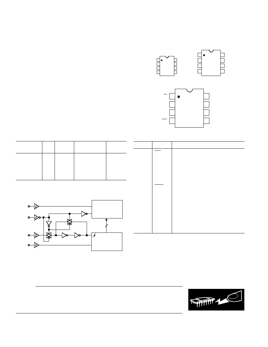
* NOTE: AD7391 HAS A 10-BIT SHIFT REGISTER
CLR
LD
CLK
SDI
RESET
LOAD
DAC
REGISTER
12-BIT AD7390*
SHIFT REGISTER
D
CLK
12
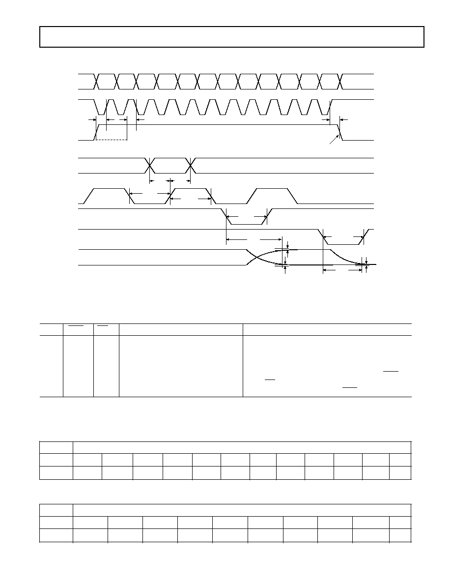
Figure 3. Digital Control Logic
PIN CONFIGURATIONS
1
2
3
4
8
7
6
TOP VIEW
(Not to Scale)
SO-8
5
TOP
VIEW
(Not to
Scale)
TSSOP-8
1
5
2
3
4
6
7
8
1
2
3
4
8
7
6
5
TOP VIEW
(Not to Scale)
LD
GND
V
OUT
V
DD
V
REF
CLK
SDI
CLR
P-DIP-8
PIN DESCRIPTIONS
Pin No.
Name
Function
1
LD
Load Strobe. Transfers shift register
data to DAC register while active low.
See truth table for operation.
2
CLK
Clock Input. Positive edge clocks data
into shift register.
3
SDI
Serial Data Input. Data loads directly
into the shift register.
4
CLR
Resets DAC register to zero condition.
Active low input.
5
GND
Analog & Digital Ground.
6
V
OUT
DAC Voltage Output. Full-scale output
1 LSB less than reference input voltage
REF.
7
V
DD
Positive Power Supply Input. Specified
range of operation 2.7 V to 5.5 V.
8
V
REF
DAC Reference Input Pin. Establishes
DAC full-scale voltage.
AD7390/AD7391
REV. 0
5
D11
D10
D9
D8
D7
D6
D5
D4
D3
D2
D1
D0
LD
CLK
SDI
t
LD1
t
LD2
t
CL
t
CH
t
DS
t
DH
SDI
CLK
CLR
t
LDW
t
CLRW
V
OUT
FS
ZS
t
S
0.1% FS
ERROR BAND
t
S
DAC REGISTER LOAD
LD
t
LD1
AD7390
AD7391
Figure 4. Timing Diagram
Table I. Control-Logic Truth Table
CLK
CLR
LD
Serial Shift Register Function
DAC Register Function
H
H
Shift-Register-Data Advanced One-Bit
Latched
X
H
L
Disables
Updated with Current Shift Register Contents
X
L
X
No Effect
Loaded with all Zeros
X
H
No Effect
Latched with all Zeros
X
L
Disabled
Previous SR Contents Loaded (Avoid usage of CLR
when LD is logic low, since SR data could be corrupted
if a clock edge takes place, while CLR returns high.)
NOTES
1
= Positive logic transition.
2
X = Don't care.
Table II. AD7390 Serial Input Register Data Format, Data is Loaded in the MSB-First Format
MSB
LSB
B11
B10
B9
B8
B7
B6
B5
B4
B3
B2
B1
B0
AD7390
D11
D10
D9
D8
D7
D6
D5
D4
D3
D2
D1
D0
Table III. AD7391 Serial Input Register Data Format, Data is Loaded in the MSB-First Format
MSB
LSB
B9
B8
B7
B6
B5
B4
B3
B2
B1
B0
AD7391
D9
D8
D7
D6
D5
D4
D3
D2
D1
D0
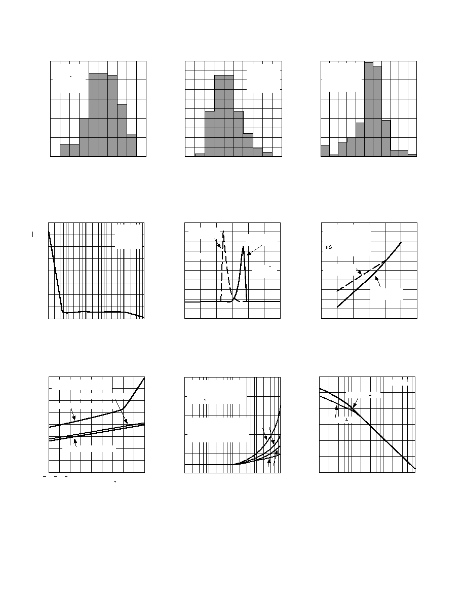
TOTAL UNADJUSTED ERROR LSB
FREQUENCY
25
0
5.0
10
5
20
15
5.8 6.6 7.3 8.1 8.9 9.7 10.5 11.2 12.0
AD7390
SS = 100 units
T
A
= 25 C
V
DD
= 2.7V
V
REF
= 2.5V
Figure 5. AD7390 Total Unadjusted
Error Histogram
FREQUENCY Hz
OUTPUT VOLTAGE NOISE µV/
Hz
10
8
0
1
10
100K
100
1K
10K
6
4
2
12
14
16
AD7390
V
DD
= 5V
V
REF
= 2.5V
T
A
= 25 C
Figure 8. Voltage Noise Density vs.
Frequency
TEMPERATURE C
SUPPLY CURRENT µA
100
20
55
35
125
15
5
25
65
85
105
45
90
60
50
40
30
80
70
AD7390
SAMPLE SIZE = 300 UNITS
V
DD
= 5.0V, V
LOGIC
= 0V
V
DD
= 3.0V, V
LOGIC
= 0V
V
DD
= 3.6V, V
LOGIC
= 2.4V
Figure 11. Supply Current vs.
Temperature
TOTAL UNADJUSTED ERROR LSB
FREQUENCY
100
0
10
40
20
80
60
3.3 3.3 10
16 23
30
36
43
50
AD7391
SS = 300 units
T
A
= 25 C
V
DD
= 2.7V
V
REF
= 2.5V
90
70
50
30
10
Figure 6. AD7391 Total Unadjusted
Error Histogram
V
IN
Volts
0.0
0.5
3.0
1.0
1.5
2.0
2.5
SUPPLY CURRENT µA
100
95
50
70
65
60
55
90
75
80
85
V
LOGIC
FROM
3.0V TO 0V
V
LOGIC
FROM
0V TO 3.0V
AD7390
T
A
= 25 C
V
DD
= 3.0V
Figure 9. Supply Current vs. Logic
Input Voltage
CLOCK FREQUENCY Hz
SUPPLY CURRENT µA
1000
800
0
1K
10K
10M
100K
1M
600
400
200
a. V
DD
= 5.5V, CODE = 155
H
b. V
DD
= 5.5V, CODE = 3FF
H
c. V
DD
= 2.7V, CODE = 155
H
d
. V
DD
= 2.7V, CODE = 355
H
a
b
c
d
AD7391
V
LOGIC
= 0V TO V
DD
TO 0V
V
REF
= 2.5V
T
A
= 25 C
Figure 12. Supply Current vs. Clock
Frequency
FULL SCALE TEMPCO ppm/
°
C
FREQUENCY
0
33
12
6
24
18
30 26 23 20 16 13 10 6 3
30
0
AD7391
SS = 100 units
T
A
= 40 to 85 C
V
DD
= 2.7V
V
REF
= 2.5V
Figure 7. AD7391 Full-Scale Output
Tempco Histogram
SUPPLY VOLTAGE V
1
2
7
3
4
5
6
THRESHOLD VOLTAGE V
5.0
4.5
0.0
2.0
1.5
1.0
0.5
4.0
2.5
3.0
3.5
V
LOGIC
FROM
HIGH TO LOW
V
LOGIC
FROM
LOW TO HIGH
AD7390
CODE = FFF
H
V
REF
= 2V
LOGIC VOLTAGE
VARIED
Figure 10. Logic Threshold vs. Supply
Voltage
FREQUENCY Hz
PSRR dB
60
50
0
10
100
10K
1K
30
20
10
40
V
DD
= 3V 5%
V
DD
= 5V 5%
T
A
= 25 C
Figure 13. Power Supply Rejection vs.
Frequency
AD7390/AD7391Typical Performance Characteristics
REV. 0
6
AD7390/AD7391
REV. 0
7
V
OUT
V
I
OUT
mA
40
30
0
0
1
5
2
3
4
20
10
V
DD
= +5V
V
REF
= +3V
CODE = ØØØ
H
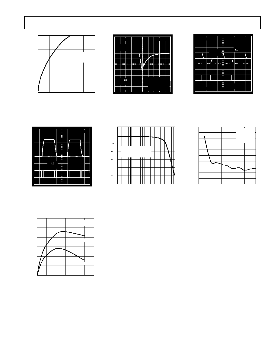
Figure 14. I
OUT
at Zero Scale vs. V
OUT
100µs
1V
TIME 100µs/div
V
OUT
(1V/DIV)
(5V/DIV)
V
DD
= 5V
V
REF
= 2.5V
f
CLK
= 50KHz
AD7390
Figure 17. Large Signal Settling Time
HOURS OF OPERATION AT 150
°
C
NOMINAL CHANGE IN VOLTAGE mV
1.2
0.0
0
100
600
200
300
400
500
1.0
0.8
0.6
0.4
0.2
AD7390
SAMPLE SIZE = 50
CODE = FFF
H
CODE = 000
H
Figure 20. Long-Term Drift
Accelerated by Burn-In
2µs
20mV
V
DD
= 5V
V
REF
= 2.5V
f
CLK
= 50KHz
CODE: 7F
H
to 80
H
TIME 2µs/DIV
AD7390
V
OUT
(5mV/DIV)
(5V/DIV)
Figure 15. Midscale Transition
Performance
FREQUENCY Hz
GAIN dB
5
0
30
10
100
100K
1K
10K
5
15
25
20
10
V
DD
= +5V
V
REF
= +100mV + 2V
DC
DATA = FFF
H
Figure 18. Reference Multiplying
Bandwidth
5µs
5mV
V
DD
= 5V
V
REF
= 2.5V
f
CLK
= 50KHz
= HIGH
TIME 5µs/DIV
V
OUT
(5mV/DIV)
CLK
(5V/DIV)
Figure 16. Digital Feedthrough
REFERENCE VOLTAGE V
0
5
1
3
2
4
INTEGRAL NONLINEARITY LSB
2.0
1.8
0.0
0.8
0.6
0.4
0.2
1.6
1.0
1.2
1.4
AD7390
V
DD
= +5V
CODE = 768
H
T
A
= 25 C
Figure 19. INL Error vs. Reference
Voltage
AD7390/AD7391
REV. 0
8
OPERATION
The AD7390 and AD7391 are a set of pin compatible, 12-bit/10-
bit digital-to-analog converters. These single-supply operation
devices consume less than 100 microamps of current while op-
erating from power supplies in the 2.7 V to 5.5 V range
making them ideal for battery operated applications. They con-
tain a voltage-switched, 12-bit/10-bit, laser-trimmed digital-to-
analog converter, rail-to-rail output op amps, serial-input
register, and a DAC register. The external reference input has
constant input resistance independent of the digital code setting
of the DAC. In addition, the reference input can be tied to the
same supply voltage as V
DD
resulting in a maximum output volt-
age span of 0 to V
DD
. The SPI compatible, serial-data interface
consists of a serial data input (SDI), clock (CLK), and load
(LD) pins. A CLR pin is available to reset the DAC register to
zero-scale. This function is useful for power-on reset or system
failure recovery to a known state.
D/A CONVERTER SECTION
The voltage switched R-2R DAC generates an output voltage
dependent on the external reference voltage connected to the
V
REF
pin according to the following equation:
Equation 1
V
OUT
= V
REF
2
N
D
where D is the decimal data word loaded into the DAC register,
and N is the number of bits of DAC resolution. In the case of
the 10-bit AD7391 using a 2.5 V reference, Equation 1
simplifies to:
Equation 2
V
OUT
= 2.5
1024
D
Using Equation 2 the nominal midscale voltage at V
OUT
is
1.25 V for D = 512; full-scale voltage is 2.497 volts. The LSB
step size is = 2.5 1/1024 = 0.0024 volts.
For the 12-bit AD7390 operating from a 5.0 V reference Equa-
tion 1 becomes:
Equation 3
V
OUT
= 5.0
4096
D
Using Equation 3 the AD7390 provides a nominal midscale
voltage of 2.5 V for D =2048, and a full-scale output of 4.998 V.
The LSB step size is = 5.0 1/4096 = 0.0012 volts.
AMPLIFIER SECTION
The internal DAC's output is buffered by a low power con-
sumption precision amplifier. The op amp has a 60
µ
s typical
settling time to 0.1% of full scale. There are slight differences in
settling time for negative slewing signals versus positive. Also,
negative transition settling time to within the last 6 LSBs of zero
volts has an extended settling time. The rail-to-rail output stage
of this amplifier has been designed to provide precision perfor-
mance while operating near either power supply. Figure 21
shows an equivalent output schematic of the rail-to-rail ampli-
fier with its N-channel pull-down FETs that will pull an output
load directly to GND. The output sourcing current is provided
by a P-channel pull-up device that can source current to GND
terminated loads.
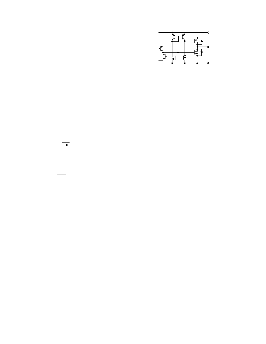
P-CH
N-CH
V
DD
V
OUT
AGND
Figure 21. Equivalent Analog Output Circuit
The rail-to-rail output stage provides 1 mA of output current.
The N-channel output pull-down MOSFET shown in Figure 21
has a 35
ON resistance, which sets the sink current capability
near ground. In addition to resistive load driving capability, the
amplifier has also been carefully designed and characterized for
up to 100 pF capacitive load driving capability.
REFERENCE INPUT
The reference input terminal has a constant input-resistance in-
dependent of digital code which results in reduced glitches on
the external reference voltage source. The high 2 M
input-
resistance minimizes power dissipation within the AD7390/
AD7391 D/A converters. The V
REF
input accepts input voltages
ranging from ground to the positive-supply voltage V
DD
. One of
the simplest applications which saves an external reference volt-
age source is connection of the V
REF
terminal to the positive
V
DD
supply. This connection results in a rail-to-rail voltage out-
put span maximizing the programmed range. The reference in-
put will accept ac signals as long as they are kept within the
supply voltage range, 0 < V
REF IN
< V
DD
. The reference
bandwidth and integral nonlinearity error performance are plot-
ted in the typical performance section, see Figures 18 and 19.
The ratiometric reference feature makes the AD7390/AD7391
an ideal companion to ratiometric analog-to-digital converters
such as the AD7896.
POWER SUPPLY
The very low power consumption of the AD7390/AD7391 is a di-
rect result of a circuit design optimizing the use of a CBCMOS
process. By using the low power characteristics of CMOS for the
logic, and the low noise, tight-matching of the complementary bi-
polar transistors, excellent analog accuracy is achieved. One ad-
vantage of the rail-to-rail output amplifiers used in the AD7390/
AD7391 is the wide range of usable supply voltage. The part is
fully specified and tested for operation from 2.7 V to 5.5 V.
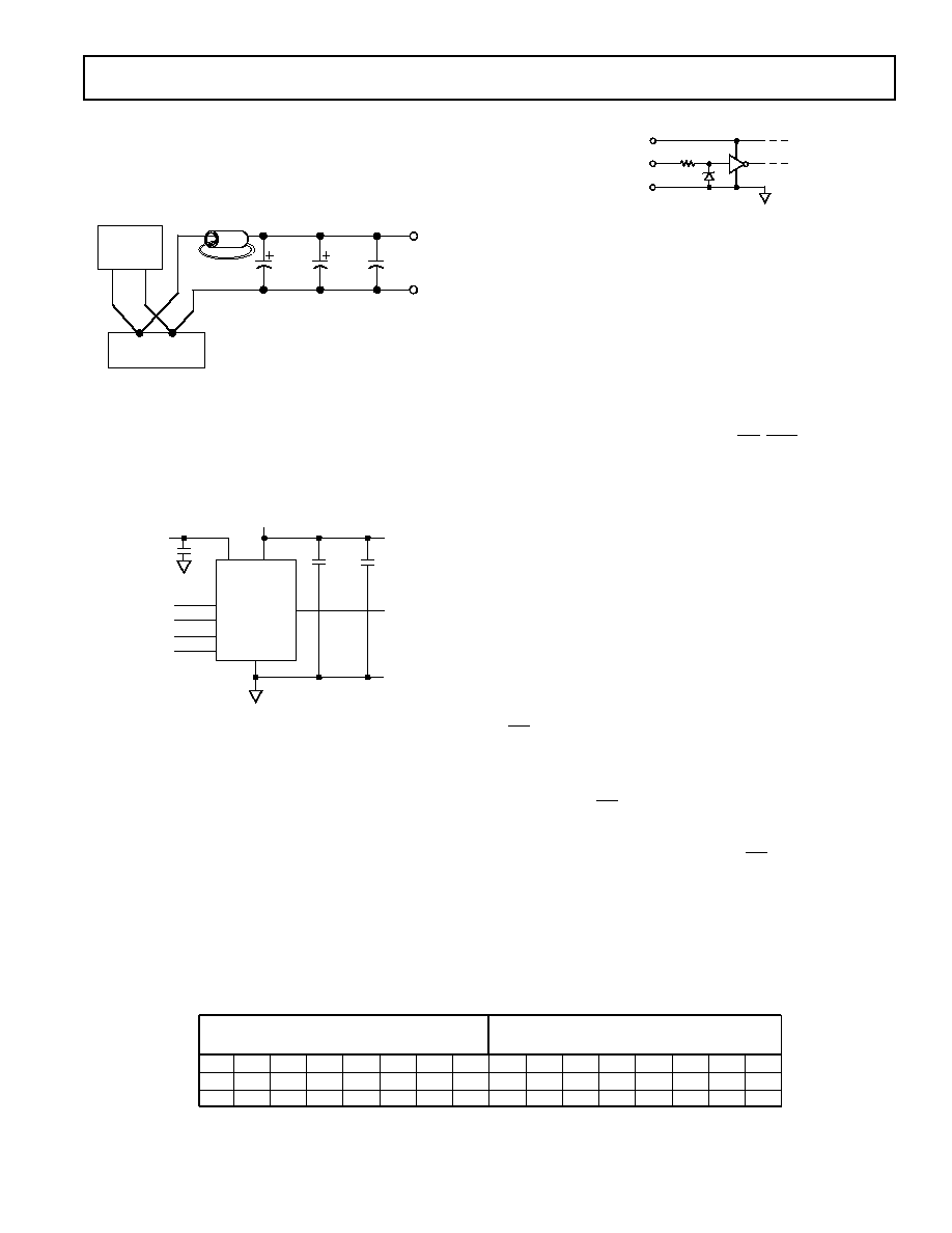
POWER SUPPLY BYPASSING AND GROUNDING
Precision analog products, such as the AD7390/AD7391, re-
quire a well filtered power source. Since the AD7390/AD7391
operates from a single 3 V to 5 V supply, it seems conve-
nient to simply tap into the digital logic power supply. Unfortu-
nately, the logic supply is often a switch-mode design, which
generates noise in the 20 kHz to 1 MHz range. In addition, fast
logic gates can generate glitches hundred of millivolts in ampli-
tude due to wiring resistance and inductance. The power supply
noise generated thereby means that special care must be taken
to assure that the inherent precision of the DAC is maintained.
Good engineering judgment should be exercised when address-
ing the power supply grounding and bypassing of the AD7390.
AD7390/AD7391
REV. 0
9
The AD7390 should be powered directly from the system power
supply. This arrangement, shown in Figure 22, employs an LC
filter and separate power and ground connections to isolate the
analog section from the logic switching transients.
100µF
ELECT.
10-22µF
TANT.
0.1µF
CER.
TTL/CMOS
LOGIC
CIRCUITS
+5V
POWER SUPPLY
+5V
+5V
RETURN
FERRITE BEAD:
2 TURNS, FAIR-RITE
#2677006301
Figure 22. Use Separate Traces to Reduce Power Supply Noise
Whether or not a separate power supply trace is available, how-
ever, generous supply bypassing will reduce supply-line induced
errors. Local supply bypassing consisting of a 10
µ
F tantalum
electrolytic in parallel with a 0.1
µ
F ceramic capacitor is recom-
mended in all applications (Figure 23).
C
+2.7V to +5.5V
0.1
µ
F
V
OUT
CLR
SDI
CLK
LD
1
2
3
4
GND
REF
V
DD
AD7390
or
AD7391
*
8
7
6
5
10
µ
F
*
OPTIONAL EXTERNAL
REFERENCE BYPASS
Figure 23. Recommended Supply Bypassing for the
AD7390/AD7391
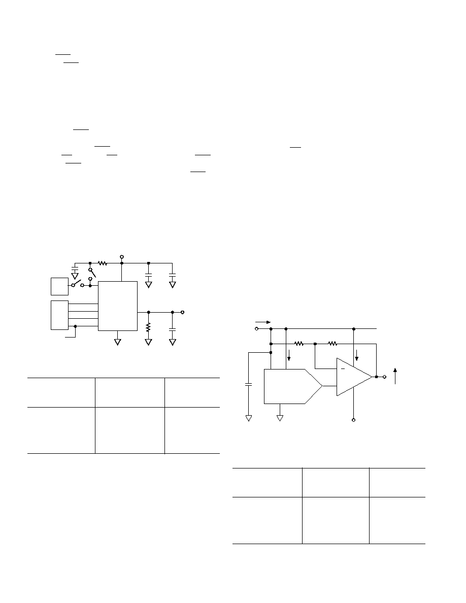
INPUT LOGIC LEVELS
All digital inputs are protected with a Zener-type ESD protec-
tion structure (Figure 24) that allows logic input voltages to ex-
ceed the V
DD
supply voltage. This feature can be useful if the
user is driving one or more of the digital inputs with a 5 V
CMOS logic input-voltage level while operating the AD7390/
AD7391 on a 3 V power supply. If this mode of interface is
used, make sure that the V
OL
of the 5 V CMOS meets the V
IL
input requirement of the AD7390/AD7391 operating at 3 V.
See Figure 10 for a graph for digital logic input threshold versus
operating V
DD
supply voltage.
V
DD
LOGIC
IN
GND
Figure 24. Equivalent Digital Input ESD Protection
In order to minimize power dissipation from input-logic levels
that are near the V
IH
and V
IL
logic input voltage specifications, a
Schmitt trigger design was used that minimizes the input-buffer
current consumption compared to traditional CMOS input
stages. Figure 9 shows a plot of incremental input voltage versus
supply current showing that negligible current consumption
takes place when logic levels are in their quiescent state. The
normal crossover current still occurs during logic transitions. A
secondary advantage of this Schmitt trigger, is the prevention of
false triggers that would occur with slow moving logic transi-
tions when a standard CMOS logic interface or opto isolators
are used. The logic inputs SDI, CLK, LD, CLR all contain the
Schmitt trigger circuits.
DIGITAL INTERFACE
The AD7390/AD7391 have a double-buffered serial data input.
The serial-input register is separate from the DAC register,
which allows preloading of a new data value into the serial regis-
ter without disturbing the present DAC values. A functional
block diagram of the digital section is shown in Figure 4, while
Table I contains the truth table for the control logic inputs.
Three pins control the serial data input. Data at the Serial Data
Input (SDI) is clocked into the shift register on the rising edge
of CLK. Data is entered in MSB-first format. Twelve clock
pulses are required to load the 12-bit AD7390 DAC value. If
additional bits are clocked into the shift register, for example
when a microcontroller sends two 8-bit bytes, the MSBs are ig-
nored (Figure 25). The CLK pin is only enabled when Load
(LD) is high. The lower resolution 10-bit AD7391 contains a
10-bit shift register. The AD7391 is also loaded MSB first with
10 bits of data. Again if additional bits are clocked into the shift
register, only the last 10 bits clocked in are used.
The Load pin (LD) controls the flow of data from the shift reg-
ister to the DAC register. After a new value is clocked into the
serial-input register, it will be transferred to the DAC register by
the negative transition of the Load pin (LD).
B15
X
X
B14
X
X
B13
X
X
B12
X
X
B11
D11
X
B10
D!0
X
B9
D9
D9
B8
D8
D8
B7
D7
D7
B6
D6
D6
B5
D5
D5
B4
D4
D4
B3
D3
D3
B2
D2
D2
B1
D1
D1
B0
D0
D0
MSB
LSB
LSB
BYTE 0
BYTE 1
MSB
D11_D0: 12-BIT AD7390 DAC VALUE; D9_D0 10-BIT AD7391 DAC VALUE
X = DON'T CARE
THE MSB OF BYTE 1 IS THE FIRST BIT THAT IS LOADED INTO THE DAC
Figure 25. Typical AD7390-Microprocessor Serial Data Input Forms
AD7390/AD7391
REV. 0
10
RESET (CLR) PIN
Forcing the CLR pin low will set the DAC register to all zeros
and the DAC output voltage will be zero volts. The reset func-
tion is useful for setting the DAC outputs to zero at power-up or
after a power supply interruption. Test systems and motor con-
trollers are two of many applications which benefit from power-
ing up to a known state. The external reset pulse can be
generated by the microprocessor's power-on RESET signal, by
an output from the microprocessor, or by an external resistor
and capacitor. CLR has a Schmitt trigger input which results in
a clean reset function when using external resistor/capacitor
generated pulses. The CLR input overrides other logic inputs,
specifically LD. However, LD should be set high before CLR
goes high. If CLR is kept low, then the contents of the shift reg-
ister will be transferred to the DAC register as soon as CLR re-
turns high. See the Control-Logic Truth Table I.
UNIPOLAR OUTPUT OPERATION
This is the basic mode of operation for the AD7390. As shown
in Figure 26, the AD7390 has been designed to drive loads as
low as 5 k
in parallel with 100 pF. The code table for this op-
eration is shown in Table IV.
+2.7V to +5.5V
0.1
µ
F
V
OUT
CLR
SDI
CLK
LD
3
2
1
4
GND
REF
V
DD
AD7390
7
6
5
10
µ
F
µ
C
RS
RL
5k
CL
100pF
EXT
REF
0.01
µ
F
R
Figure 26. AD7390 Unipolar Output Operation
Table IV. AD7390 Unipolar Code Table
Hexadecimal
Decimal
Output
Number
Number
Voltage (V)
in DAC Register
in DAC Register
V
REF
= 2.5 V
FFF
4095
2.4994
801
2049
1.2506
800
2048
1.2500
7FF
2047
1.2494
000
0
0
The circuit can be configured with an external reference plus
power supply, or powered from a single dedicated regulator or ref-
erence depending on the application performance requirements.
BIPOLAR OUTPUT OPERATION
Although the AD7391 has been designed for single-supply op-
eration, the output can be easily configured for bipolar opera-
tion. A typical circuit is shown in Figure 27. This circuit uses a
clean regulated 5 V supply for power, which also provides the
circuit's reference voltage. Since the AD7391 output span
swings from ground to very near 5 V, it is necessary to choose
an external amplifier with a common-mode input voltage range
that extends to its positive supply rail. The micropower con-
sumption OP196 has been designed just for this purpose and re-
sults in only 50 microamps of maximum current consumption.
Connection of the equal valued 470 k
resistors results in a dif-
ferential amplifier mode of operation with a voltage gain of two,
which results in a circuit output span of ten volts, that is, 5 V
to 5 V. As the DAC is programmed with zero-code 000
H
to
midscale 200
H
to full-scale 3FF
H
, the circuit output voltage V
O
is set at 5 V, 0 V and 5 V (minus 1 LSB). The output volt-
age V
O
is coded in offset binary according to Equation 4.
Equation 4
V
O
=
5
1
512
D
where D is the decimal code loaded in the AD7391 DAC regis-
ter. Note that the LSB step size is 10/1024 = 10 mV. This cir-
cuit has been optimized for micropower consumption including
the 470 k
gain setting resistors, which should have low tem-
perature coefficients to maintain accuracy and matching (prefer-
ably the same material, such as metal film). If better stability is
required the power supply could be substituted with a precision
reference voltage such as the low dropout REF195, which can
easily supply the circuit's 162
µ
A of current, and still provide
additional power for the load connected to V
O
. The micropower
REF195 is guaranteed to source 10 mA output drive current,
but only consumes 50
µ
A internally. If higher resolution is re-
quired, the AD7390 can be used with the addition of two more
bits of data inserted into the software coding, which would re-
sult in a 2.5 mV LSB step size. Table V shows examples of
nominal output voltages V
O
provided by the Bipolar Operation
circuit application.
DIGITAL INTERFACE CIRCUITRY OMITTED FOR CLARITY
OP196
BIPOLAR
OUTPUT
SWING
5V
5V
V
O
< 50
µ
A
5V
AD7391
V
OUT
GND
REF
V
DD
C
470k
470k
5V
< 100
µ
A
I
SY
< 162
µ
A
Figure 27. Bipolar Output Operation
Table V. Bipolar Code Table
Hexadecimal
Decimal
Analog
Number
Number
Output
In DAC Register
in DAC Register
Voltage (V)
3FF
1023
4.9902
201
513
0.0097
200
512
0.0000
1FF
511
-0.0097
000
0
-5.0000

AD7390/AD7391
REV. 0
11
MICROCOMPUTER INTERFACES
The AD7390 serial data input provides an easy interface to a va-
riety of single-chip microcomputers (
µ
Cs). Many
µ
Cs have a
built-in serial data capability which can be used for communi-
cating with the DAC. In cases where no serial port is provided,
or it is being used for some other purpose (such as an RS-232
communications interface), the AD7390/AD7391 can easily be
addressed in software.
Twelve data bits are required to load a value into the AD7390.
If more than 12 bits are transmitted before the load LD input
goes high, the extra (i.e., the most-significant) bits are ignored.
This feature is valuable because most
µ
Cs only transmit data in
8-bit increments. Thus, the
µ
C sends 16 bits to the DAC in-
stead of 12 bits. The AD7390 will only respond to the last
12 bits clocked into the SDI input, however, so the serial-data
interface is not affected.
Ten data bits are required to load a value into the AD7391. If
more than 10 bits are transmitted before load LD returns high,
the extra bits are ignored.
AD7390/AD7391
REV. 0
12
OUTLINE DIMENSIONS
Dimensions shown in inches and (mm).
PRINTED IN U.S.A.
8-Lead SOIC (SO-8)
0.1968 (5.00)
0.1890 (4.80)
8
5
4
1
0.2440 (6.20)
0.2284 (5.80)
PIN 1
0.1574 (4.00)
0.1497 (3.80)
0.0688 (1.75)
0.0532 (1.35)
SEATING
PLANE
0.0098 (0.25)
0.0040 (0.10)
0.0192 (0.49)
0.0138 (0.35)
0.0500
(1.27)
BSC
0.0098 (0.25)
0.0075 (0.19)
0.0500 (1.27)
0.0160 (0.41)
8
°
0
°
0.0196 (0.50)
0.0099 (0.25)
x 45
°
8-Pin Plastic DIP (N-8)
8
1
4
5
0.430 (10.92)
0.348 (8.84)
0.280 (7.11)
0.240 (6.10)
PIN 1
SEATING
PLANE
0.022 (0.558)
0.014 (0.356)
0.060 (1.52)
0.015 (0.38)
0.210 (5.33)
MAX
0.130
(3.30)
MIN
0.070 (1.77)
0.045 (1.15)
0.100
(2.54)
BSC
0.160 (4.06)
0.115 (2.93)
0.325 (8.25)
0.300 (7.62)
0.015 (0.381)
0.008 (0.204)
0.195 (4.95)
0.115 (2.93)
8-Pin TSSOP (RU-8)
8
5
4
1
0.122 (3.10)
0.114 (2.90)
0.256 (6.50)
0.246 (6.25)
0.177 (4.50)
0.169 (4.30)
PIN 1
0.0256 (0.65)
BSC
SEATING
PLANE
0.006 (0.15)
0.002 (0.05)
0.0118 (0.30)
0.0075 (0.19)
0.0433
(1.10)
MAX
0.0079 (0.20)
0.0035 (0.090)
0.028 (0.70)
0.020 (0.50)
8
°
0
°
C2151187/96