Äîêóìåíòàöèÿ è îïèñàíèÿ www.docs.chipfind.ru
REV. 0
Information furnished by Analog Devices is believed to be accurate and
reliable. However, no responsibility is assumed by Analog Devices for its
use, nor for any infringements of patents or other rights of third parties that
may result from its use. No license is granted by implication or otherwise
under any patent or patent rights of Analog Devices. Trademarks and
registered trademarks are the property of their respective owners.
One Technology Way, P.O. Box 9106, Norwood, MA 02062-9106, U.S.A.
Tel: 781/329-4700
www.analog.com
Fax: 781/326-8703
© 2003 Analog Devices, Inc. All rights reserved.
AD5424/AD5433/AD5445
*
8-/10-/12-Bit, High Bandwidth,
Multiplying DACs with Parallel Interface
*U.S. Patent No. 5,689,257
FEATURES
2.5 V to 5.5 V Supply Operation
Fast Parallel Interface (17 ns Write Cycle)
10 MHz Multiplying Bandwidth
10 V Reference Input
Extended Temperature Range 40 C to +125 C
20-Lead TSSOP and Chip Scale (4 mm 4 mm) Packages
8-, 10-, and 12-Bit Current Output DACs
Upgrades to AD7524/AD7533/AD7545
Pin Compatible 8-, 10-, and 12-Bit DACs in Chip Scale
Guaranteed Monotonic
4-Quadrant Multiplication
Power-On Reset with Brownout Detection
Readback Function
0.4 A Typical Power Consumption
APPLICATIONS
Portable Battery-Powered Applications
Waveform Generators
Analog Processing
Instrumentation Applications
Programmable Amplifiers and Attenuators
Digitally-Controlled Calibration
Programmable Filters and Oscillators
Composite Video
Ultrasound
Gain, Offset, and Voltage Trimming
GENERAL DESCRIPTION
The AD5424/AD5433/AD5445 are CMOS 8-, 10-, and 12-bit
current output digital-to-analog converters (DACs), respectively.
These devices operate from a 2.5 V to 5.5 V power supply,
making them suited to battery-powered applications and many
other applications.
These DACs utilize data readback allowing the user to read the
contents of the DAC register via the DB pins. On power-up, the
internal register and latches are filled with 0s and the DAC
outputs are at zero scale.
As a result of manufacture on a CMOS submicron process, they
offer excellent 4-quadrant multiplication characteristics, with
large signal multiplying bandwidths of up to 10 MHz.
The applied external reference input voltage (V
REF
) determines
the full-scale output current. An integrated feedback resistor
(R
FB
) provides temperature tracking and full-scale voltage output
when combined with an external I-to-V precision amplifier.
While these devices are upgrades of AD7524/AD7533/AD7545
in multiplying bandwidth performance, they have a latched
interface and cannot be used in transparent mode.
The AD5424 is available in small 20-lead LFCSP and 16-lead
TSSOP packages, while the AD5433/AD5445 DACs are avail-
able in small 20-lead LFCSP and TSSOP packages.
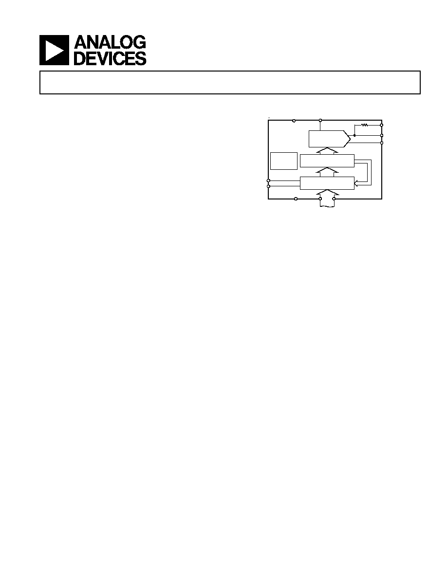
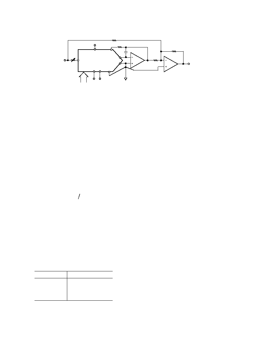
FUNCTIONAL BLOCK DIAGRAM
R/
W
CS
AD5424/
AD5433/
AD5445
V
REF
I
OUT
2
I
OUT
1
R
FB
R
8-/10-/12-BIT
R-2R DAC
DAC REGISTER
INPUT LATCH
V
DD
POWER-ON
RESET
DB0
DB7/DB9/DB11
DATA
INPUTS
GND

REV. 0
2
AD5424/AD5433/AD5445SPECIFICATIONS
1
Parameter
Min
Typ
Max
Unit
Conditions
STATIC PERFORMANCE
AD5424
Resolution
8
Bits
Relative Accuracy
±0.25 LSB
Differential Nonlinearity
±0.5
LSB
Guaranteed monotonic
AD5433
Resolution
10
Bits
Relative Accuracy
±0.5
LSB
Differential Nonlinearity
±1
LSB
Guaranteed monotonic
AD5445
Resolution
12
Bits
Relative Accuracy
±1
LSB
Differential Nonlinearity
1/+2
LSB
Guaranteed monotonic
Gain Error
±10
mV
Gain Error Temperature Coefficient
2
±5
ppm FSR/ C
Output Leakage Current
2
±10
nA
Data = 0x0000, T
A
= 25 C, I
OUT
1
±20
nA
Data = 0x0000, I
OUT
1
REFERENCE INPUT
2
Reference Input Range
±10
V
V
REF
Input Resistance
8
10
12
k
Input resistance TC = 50 ppm/ C
R
FB
Resistance
8
10
12
k
Input resistance TC = 50 ppm/ C
Input Capacitance
Code 0
3
6
pF
Code 4095
5
8
pF
DIGITAL INPUTS/OUTPUT
2
Input High Voltage, V
IH
1.7
V
Input Low Voltage, V
IL
0.6
V
Input Leakage Current, I
IL
1
A
Input Capacitance
4
10
pF
V
DD
= 4.5 V to 5.5 V
Output Low Voltage, V
OL
0.4
V
I
SINK
= 200
µA
Output High Voltage, V
OH
V
DD
1
V
I
SOURCE
= 200
µA
V
DD
= 2.5 V to 3.6 V
Output Low Voltage, V
OL
0.4
V
I
SINK
= 200
µA
Output High Voltage, V
OH
V
DD
0.5
V
I
SOURCE
= 200
µA
DYNAMIC PERFORMANCE
2
Reference Multiplying Bandwidth
10
MHz
V
REF
=
±3.5 V; DAC loaded all 1s
Output Voltage Settling Time
V
REF
= 10 V, R
LOAD
= 100
, C
LOAD
= 15 pF
AD5424
30
60
ns
Measured to
±16 mV of full scale
AD5433
35
70
ns
Measured to
±4 mV of full scale
AD5445
80
120
ns
Measured to
±1 mV of full scale
Digital Delay
20
40
ns
Interface delay time
10%
to 90% Settling Time
15
30
ns
Rise and Fall time, V
REF
= 10 V, R
LOAD
= 100
Digital to Analog Glitch Impulse
2
nV-s
1 LSB change around major carry, V
REF
= 0 V
Multiplying Feedthrough Error
DAC latch loaded with all 0s. V
REF
=
±3.5 V
70
dB
Reference = 1 MHz
48
dB
Reference = 10 MHz
(V
DD
= 2.5 V to 5.5 V, V
REF
= 10 V, I
OUT
2 = O V. All specifications T
MIN
to T
MAX
, unless otherwise noted. DC performance measured with OP1177,
AC performance with AD8038, unless otherwise noted.)

REV. 0
AD5424/AD5433/AD5445
3
Parameter
Min
Typ
Max
Unit
Conditions
Output Capacitance
I
OUT
2
22
25
pF
All 0s loaded
10
12
pF
All 1s loaded
I
OUT
1
12
17
pF
All 0s loaded
25
30
pF
All 1s loaded
Digital Feedthrough
1
nV-s
Feedthrough to DAC output with
CS high and
alternate loading of all 0s and all 1s
Total Harmonic Distortion
81
dB
V
REF
= 3.5 V pk-pk; all 1s loaded, f = 100 kHz
Digital THD
Clock = 10 MHz
50 kHz f
OUT
65
dB
Output Noise Spectral Density
25
nV
Hz
@ 1 kHz
SFDR Performance (Wide Band)
AD5445, 65k codes, V
REF
= 3.5 V
Clock = 10 MHz
500 kHz f
OUT
55
dB
100 kHz f
OUT
63
dB
50 kHz f
OUT
65
dB
Clock = 25 MHz
500 kHz f
OUT
50
dB
100 kHz f
OUT
60
dB
50 kHz f
OUT
62
dB
SFDR Performance (Narrow Band)
AD5445, 65k codes, V
REF
= 3.5 V
Clock = 10 MHz
500 kHz f
OUT
73
dB
100 kHz f
OUT
80
dB
50 kHz f
OUT
87
dB
Clock = 25 MHz
500 kHz f
OUT
70
dB
100 kHz f
OUT
75
dB
50 kHz f
OUT
80
dB
Intermodulation Distortion
AD5445, 65k codes, V
REF
= 3.5 V
Clock = 10 MHz
f
1
= 400 kHz, f
2
= 500 kHz
65
dB
f
1
= 40 kHz, f
2
= 50 kHz
72
dB
Clock = 25 MHz
f
1
= 400 kHz, f
2
= 500 kHz
51
dB
f
1
= 40 kHz, f
2
= 50 kHz
65
dB
POWER REQUIREMENTS
Power Supply Range
2.5
5.5
V
I
DD
0.6
A
T
A
= 25 C, logic inputs = 0 V or V
DD
0.4
5
A
Logic inputs = 0 V or V
DD
NOTES
1
Temperature range is as follows: Y version: 40 C to +125 C.
2
Guaranteed by design, not subject to production test.
Specifications subject to change without notice.
REV. 0
4
AD5424/AD5433/AD5445
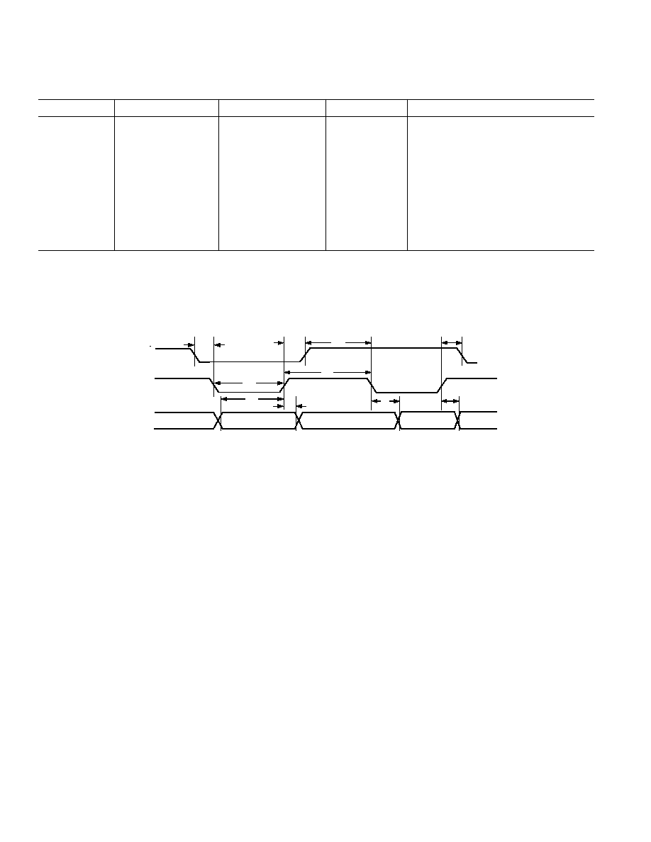
t
5
DATA VALID
t
4
t
2
CS
R/
W
DATA
t
1
DATA VALID
t
2
t
9
t
8
t
3
t
6
t
7
Figure 1. Timing Diagram
TIMING CHARACTERISTICS
1, 2
Parameter
V
DD
= 2.5 V to 5.5 V
V
DD
= 4.5 V to 5.5 V
Unit
Conditions/Comments
t
1
0
0
ns min
R/
W to CS setup time
t
2
0
0
ns min
R/
W to CS hold time
t
3
10
10
ns min
CS low time (write cycle)
t
4
6
6
ns min
Data setup time
t
5
0
0
ns min
Data hold time
t
6
5
5
ns min
R/
W high to CS low
t
7
9
7
ns min
CS min high time
t
8
20
10
ns typ
Data access time
40
20
ns max
t
9
5
5
ns typ
Bus relinquish time
10
10
ns max
NOTES
1
See Figure 1.
Temperature range is as follows: Y version: 40 C to +125 C.
Guaranteed by design and characterization, not subject to production test.
2
All input signals are specified with tr = tf = 1 ns (10% to 90% of V
DD
) and timed from a voltage level of (V
IL
+ V
IH
)/2. Digital output timing measured with load
circuit in Figure 2.
Specifications subject to change without notice.
(V
REF
= 5 V, I
OUT
2 = O V. All specifications T
MIN
to T
MAX
, unless otherwise noted.)
REV. 0
AD5424/AD5433/AD5445
5
ABSOLUTE MAXIMUM RATINGS
1
(T
A
= 25 C, unless otherwise noted.)
V
DD
to GND . . . . . . . . . . . . . . . . . . . . . . . . . . . 0.3 V to +7 V
V
REF
,
R
FB
to GND . . . . . . . . . . . . . . . . . . . . . . 12 V to +12 V
I
OUT
1, I
OUT
2 to GND . . . . . . . . . . . . . . . . . . . . 0.3 V to +7 V
Logic Inputs and Output
2
. . . . . . . . . . . 0.3 V to V
DD
+0.3 V
Operating Temperature Range
Extended Industrial (Y Version) . . . . . . . . 40 C to +125 C
Storage Temperature Range . . . . . . . . . . . . . 65 C to +150 C
Junction Temperature . . . . . . . . . . . . . . . . . . . . . . . . . . 150 C
16-Lead TSSOP
JA
Thermal Impedance . . . . . . . . . 150 C/W
20-Lead TSSOP
JA
Thermal Impedance . . . . . . . . . 143 C/W
20-Lead LFCSP
JA
Thermal Impedance . . . . . . . . . 135 C/W
Lead Temperature, Soldering (10 seconds) . . . . . . . . . . 300 C
IR Reflow, Peak Temperature (<20 seconds) . . . . . . . . 235 C
NOTES
1
Stresses above those listed under Absolute Maximum Ratings may cause perma-
nent damage to the device. This is a stress rating only and functional operation of
the device at these or any other conditions above those listed in the operational
sections of this specification is not implied. Exposure to absolute maximum rating
conditions for extended periods may affect device reliability. Only one absolute
maximum rating may be applied at any one time.
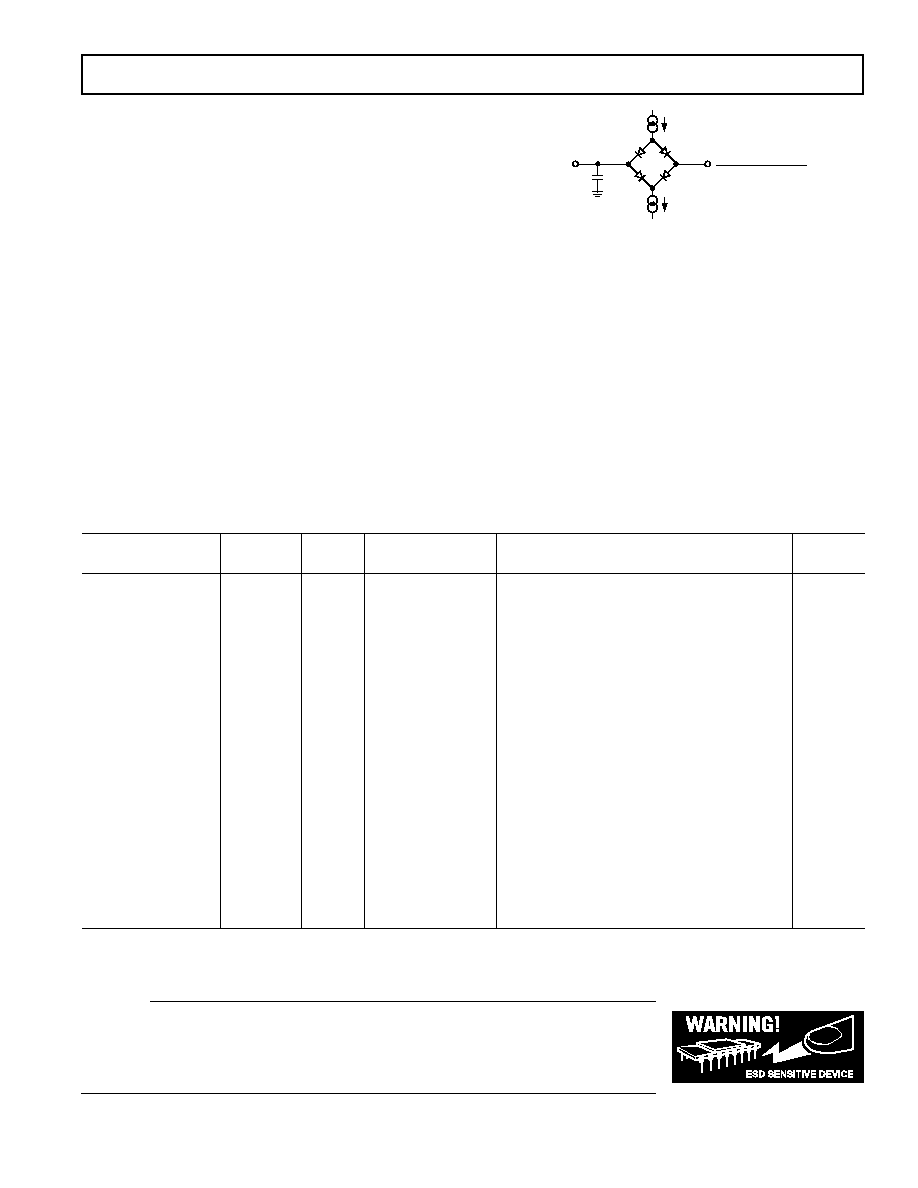
2
Overvoltages at DBx,
CS, and R/W, will be clamped by internal diodes.
I
OL
200 A
I
OH
200 A
C
L
50pF
TO
OUTPUT
PIN
V
OH (MIN)
+ V
OL (MAX)
2
Figure 2. Load Circuit for Data Output Timing Specifications
ORDERING GUIDE
Resolution INL
Temperature
Package
Model
(Bits)
(LSB)
Range
Package Description
Option
AD5424YRU
8
±0.25
40 C to +125 C
TSSOP (Thin Shrink Small Outline Package)
RU-16
AD5424YRU-REEL
8
±0.25
40 C to +125 C
TSSOP (Thin Shrink Small Outline Package)
RU-20
AD5424YRU-REEL7
8
±0.25
40 C to +125 C
TSSOP (Thin Shrink Small Outline Package)
RU-20
AD5424YCP
8
±0.25
40 C to +125 C
LFCSP (Chip Scale Package)
CP-20
AD5424YCP-REEL
8
±0.25
40 C to +125 C
LFCSP (Chip Scale Package)
CP-20
AD5424YCP-REEL7
8
±0.25
40 C to +125 C
LFCSP (Chip Scale Package)
CP-20
AD5433YRU
10
±0.5
40 C to +125 C
TSSOP (Thin Shrink Small Outline Package)
RU-20
AD5433YRU-REEL
10
±0.5
40 C to +125 C
TSSOP (Thin Shrink Small Outline Package)
RU-20
AD5433YRU-REEL7
10
±0.5
40 C to +125 C
TSSOP (Thin Shrink Small Outline Package)
RU-20
AD5433YCP
10
±0.5
40 C to +125 C
LFCSP (Chip Scale Package)
CP-20
AD5433YCP-REEL
10
±0.5
40 C to +125 C
LFCSP (Chip Scale Package)
CP-20
AD5433YCP-REEL7
10
±0.5
40 C to +125 C
LFCSP (Chip Scale Package)
CP-20
AD5445YRU
12
±1
40 C to +125 C
TSSOP (Thin Shrink Small Outline Package)
RU-20
AD5445YRU-REEL
12
±1
40 C to +125 C
TSSOP (Thin Shrink Small Outline Package)
RU-20
AD5445YRU-REEL7
12
±1
40 C to +125 C
TSSOP (Thin Shrink Small Outline Package)
RU-20
AD5445YCP
12
±1
40 C to +125 C
LFCSP (Chip Scale Package)
CP-20
AD5445YCP-REEL
12
±1
40 C to +125 C
LFCSP (Chip Scale Package)
CP-20
AD5445YCP-REEL7
12
±1
40 C to +125 C
LFCSP (Chip Scale Package)
CP-20
EVAL-AD5424EB
Evaluation Kit
EVAL-AD5433EB
Evaluation Kit
EVAL-AD5445EB
Evaluation Kit
CAUTION
ESD (electrostatic discharge) sensitive device. Electrostatic charges as high as 4000 V readily
accumulate on the human body and test equipment and can discharge without detection. Although the
AD5424/AD5433/AD5445 features proprietary ESD protection circuitry, permanent damage may
occur on devices subjected to high energy electrostatic discharges. Therefore, proper ESD precautions
are recommended to avoid performance degradation or loss of functionality.
REV. 0
6
AD5424/AD5433/AD5445
TSSOP
AD5424
(Not to Scale)
I
OUT
1
I
OUT
2
GND
DB7
DB6
1
2
3
4
5
16
9
10
DB1
DB2
R
FB
DB5
DB4
DB3
6
7
8
11
12
13
14
15
V
REF
V
DD
R/
W
CS
DB0 (LSB)
LFCSP
PIN 1
INDICATOR
TOP VIEW
AD5424
1
GND
2
DB7
3
DB6
4
DB5
5
DB4
DB3 6
DB2 7
DB1 8
DB0 9
NC 10
15 R/
W
14
CS
13 NC
12 NC
11 NC
20 I
OUT
2
19 I
OUT
1
18 R
FB
17 V
REF
16 V
DD
NC = NO CONNECT
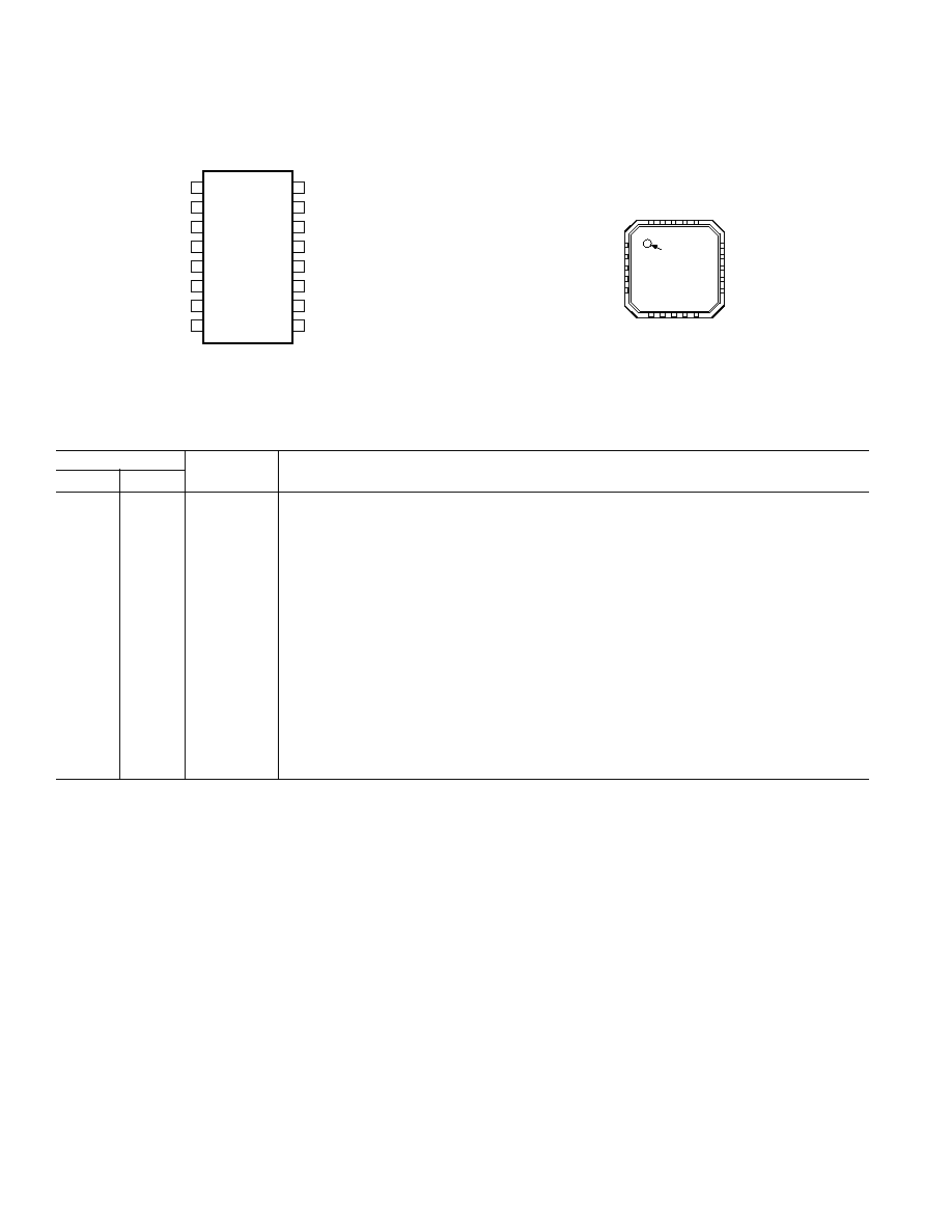
PIN CONFIGURATIONS
AD5424 PIN FUNCTION DESCRIPTIONS
Pin No.
TSSOP
LFCSP
Mnemonic
Function
1
19
I
OUT
1
DAC Current Output.
2
20
I
OUT
2
DAC Analog Ground. This pin should normally be tied to the analog ground of the system.
3
1
GND
Ground
411
29
DB7DB0
Parallel Data Bits 7 to 0.
1013
NC
No Internal Connection.
12
14
CS
Chip Select Input. Active low. Used in conjunction with R/
W to load parallel data to the input
latch or to read data from the DAC register. Rising edge of
CS loads data.
13
15
R/
W
Read/Write. When low, used in conjunction with
CS to load parallel data. When high, use
with
CS to readback contents of DAC register.
14
16
V
DD
Positive Power Supply Input. These parts can be operated from a supply of 2.5 V to 5.5 V.
15
17
V
REF
DAC Reference Voltage Input Terminal.
16
18
R
FB
DAC Feedback Resistor Pin. Establish voltage output for the DAC by connecting to external
amplifier output.
REV. 0
AD5424/AD5433/AD5445
7
TSSOP
I
OUT
1
I
OUT
2
GND
DB9
DB6
1
2
3
4
5
20
14
NC
R
FB
DB5
DB4
DB3
6
7
8
15
16
17
18
19
V
REF
V
DD
R/
W
CS
DB0 (LSB)
NC = NO CONNECT
12
DB1
DB2
9
10
13
11
DB8
DB7
NC
AD5433
(Not to Scale)
LFCSP
PIN 1
INDICATOR
TOP VIEW
AD5433
1
GND
2
DB9
3
DB8
4
DB7
5
DB6
DB5 6
DB4 7
DB3 8
DB2 9
DB1 10
15 R/
W
14
CS
13 NC
12 NC
11 DB0
20 I
OUT
2
19 I
OUT
1
18 R
FB
17 V
REF
16 V
DD
NC = NO CONNECT
PIN CONFIGURATIONS
AD5433 PIN FUNCTION DESCRIPTIONS
Pin No.
TSSOP
LFCSP
Mnemonic Function
1
19
I
OUT
1
DAC Current Output.
2
20
I
OUT
2
DAC Analog Ground. This pin should normally be tied to the analog ground of the system.
3
1
GND
Ground
413
211
DB9DB0
Parallel Data Bits 9 to 0.
14, 15
12, 13
NC
Not Internally Connected.
16
14
CS
Chip Select Input. Active low. Used in conjunction with R/
W to load parallel data to the input
latch or to read data from the DAC register. Rising edge of
CS loads data.
17
15
R/
W
Read/Write. When low, used in conjunction with
CS to load parallel data. When high, use
with
CS to readback contents of DAC register.
18
16
V
DD
Positive Power Supply Input. These parts can be operated from a supply of 2.5 V to 5.5 V.
19
17
V
REF
DAC Reference Voltage Input Terminal.
20
18
R
FB
DAC Feedback Resistor Pin. Establish voltage output for the DAC by connecting to external
amplifier output.
REV. 0
8
AD5424/AD5433/AD5445
TSSOP
I
OUT
1
I
OUT
2
GND
DB9
DB6
1
2
3
4
5
20
14
R
FB
DB5
6
7
8
15
16
17
18
19
V
REF
V
DD
R/
W
CS
12
DB3
DB4
9
10
13
11
DB8
DB7
AD5445
(Not to Scale)
DB11
DB10
DB0 (LSB)
DB1
DB2
LFCSP
PIN 1
INDICATOR
TOP VIEW
AD5445
1
GND
2
DB11
3
DB10
4
DB9
5
DB8
DB7 6
DB6 7
DB5 8
DB4 9
DB3 10
15 R/
W
14
CS
13 DB0
12 DB1
11 DB2
20 I
OUT
2
19 I
OUT
1
18 R
FB
17 V
REF
16 V
DD
PIN CONFIGURATIONS
AD5445 PIN FUNCTION DESCRIPTIONS
Pin No.
TSSOP
LFCSP Mnemonic
Function
1
19
I
OUT
1
DAC Current Output.
2
20
I
OUT
2
DAC Analog Ground. This pin should normally be tied to the analog ground of the system.
3
1
GND
Ground Pin.
415
213
DB11DB0
Parallel Data Bits 11 to 0.
16
14
CS
Chip Select Input. Active low. Rising edge of
CS loads data. Used in conjunction with R/W to
load parallel data to the input latch or to read data from the DAC register.
17
15
R/
W
Read/Write. When low, used in conjunction with
CS to load parallel data. When high, use with
CS to readback contents of DAC register.
18
16
V
DD
Positive Power Supply Input. These parts can be operated from a supply of +2.5 V to +5.5 V.
19
17
V
REF
DAC Reference Voltage Input Terminal.
20
18
R
FB
DAC Feedback Resistor Pin. Establish voltage output for the DAC by connecting to external
amplifier output.
REV. 0
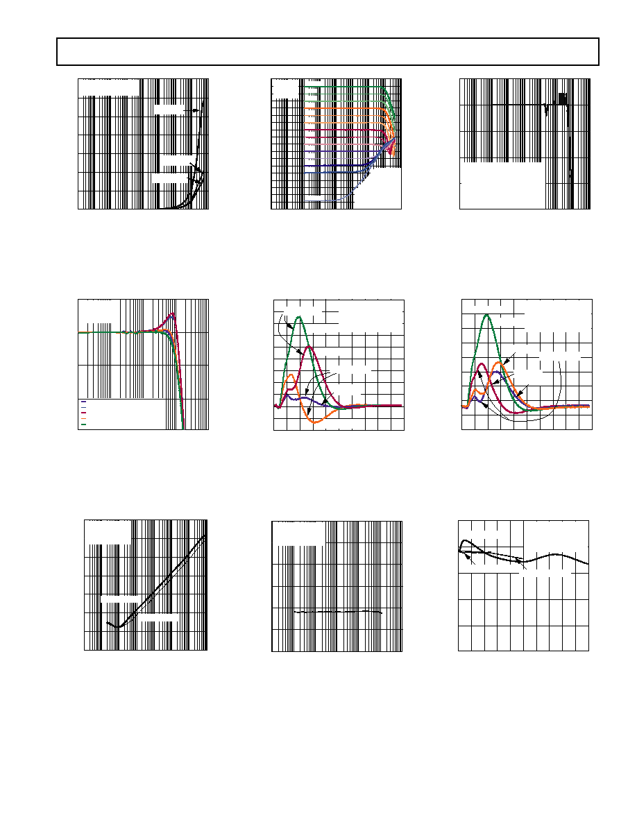
Typical Performance CharacteristicsAD5424/AD5433/AD5445
9
CODE
INL (LSB)
0.20
0.10
0.15
0
0.05
0.05
0.10
0.15
0.20
0
50
100
150
250
200
T
A
= 25 C
V
REF
= 10V
V
DD
= 5V
TPC 1. INL vs. Code (8-Bit DAC)
CODE
DNL (LSB)
0.20
0.15
0.10
0.05
0.10
0.05
0
0.15
0.20
0
50
100
150
200
250
T
A
= 25 C
V
REF
= 10V
V
DD
= 5V
TPC 4. DNL vs. Code (8-Bit DAC)
REFERENCE VOLTAGE
INL (LSB)
0.6
0.5
0.4
0.3
0.2
0.1
0
0.1
0.2
0.3
2
3
4
5
6
7
8
9
10
MAX INL
MIN INL
T
A
= 25 C
V
REF
= 10V
V
DD
= 5V
TPC 7. INL vs. Reference Voltage,
AD5445
CODE
INL (LSB)
0.5
0.4
0.3
0.2
0.1
0
0.5
0.4
0.3
0.2
0.1
0
200
400
800
600
1000
T
A
= 25 C
V
REF
= 10V
V
DD
= 5V
TPC 2. INL vs. Code (10-Bit DAC)
CODE
DNL (LSB)
0.5
0.4
0.3
0.1
0.2
0
0.1
0.2
0.3
0.4
0.5
0
200
400
800
600
1000
T
A
= 25 C
V
REF
= 10V
V
DD
= 5V
TPC 5. DNL vs. Code (10-Bit DAC)
REFERENCE VOLTAGE
DNL (LSB)
0.40
0.45
0.50
0.55
0.60
0.65
0.70
2
3
4
5
6
7
8
9
10
MIN DNL
T
A
= 25 C
V
REF
= 10V
V
DD
= 5V
TPC 8. DNL vs. Reference Voltage,
AD5445
CODE
INL (LSB)
1.0
0.8
0.6
0.4
0.2
0
0.2
0.4
0.6
0.8
1.0
0
500 1000 1500 2000 2500 3000 3500 4000
T
A
= 25 C
V
REF
= 10V
V
DD
= 5V
TPC 3. INL vs. Code (12-Bit DAC)
CODE
DNL (LSB)
1.0
0.2
0.8
0.6
0.4
0.2
0.4
0.6
0
0.8
1.0
0
500 1000
2000 2500 3000 3500
1500
4000
T
A
= 25 C
V
REF
= 10V
V
DD
= 5V
TPC 6. DNL vs. Code (12-Bit DAC)
TEMPERATURE ( C)
ERROR (mV)
5
4
3
4
0
2
3
2
5
60 40 20
0
20
40
60
80 100 120 140
1
1
V
DD
= 5V
V
DD
= 2.5V
V
REF
= 10V
TPC 9. Gain Error vs. Temperature
REV. 0
10
AD5424/AD5433/AD5445
V
BIAS
(V)
LSB
2.0
1.5
1.0
1.5
0
0.5
1.0
0.5
2.0
0.5 0.6 0.7 0.8 0.9 1.0 1.1 1.2 1.3 1.4 1.5
T
A
= 25 C
V
REF
= 0V
V
DD
= 3V
MAX INL
MIN INL
MAX DNL
MIN DNL
TPC 10. Linearity vs. V
BIAS
Voltage
Applied to I
OUT
2, AD5445
T
A
= 25 C
V
REF
= 2.5V
V
DD
= 3V AND 5V
GAIN ERROR
OFFSET ERROR
VOLTAGE (mV)
0.5
0.2
0.3
0.4
0.1
0
0.3
0.4
0.2
0.1
0.5
V
BIAS
(V)
0
0.2 0.4 0.6 0.8 1.0 1.2 1.4 1.6 1.8 2.0
TPC 13. Gain and Offset Errors
vs. V
BIAS
Voltage Applied to I
OUT
2
INPUT VOLTAGE (V)
CURRENT (mA)
8
5
0
5.0
7
6
3
1
4
2
4.5
4.0
3.5
3.0
2.5
2.0
1.5
1.0
0.5
0
T
A
= 25 C
V
DD
= 5V
V
DD
= 3V
V
DD
= 2.5V
TPC 16. Supply Current vs. Logic
Input Voltage (Driving DB0DB11,
All Other Digital Inputs @ Supplies)
V
BIAS
(V)
LSB
4
2
3
4
1
0
3
2
1
5
0
0.2 0.4 0.6 0.8 1.0 1.2 1.4 1.6 1.8 2.0
T
A
= 25 C
V
REF
= 2.5V
V
DD
= 3V
MAX INL
MIN INL
MAX DNL
MIN DNL
TPC 11. Linearity vs. V
BIAS
Voltage
Applied to I
OUT
2, AD5445
V
BIAS
(V)
LSB
3
0
1
2
1
2
3
0.5
1.0
1.5
2.0
2.5
T
A
= 25 C
V
REF
= 0V
V
DD
= 5V
MAX INL
MIN INL
MAX DNL
MIN DNL
TPC 14. Linearity vs. V
BIAS
Voltage
Applied to I
OUT
2, AD5445
0
0.2
0.4
0.6
0.8
1.0
1.2
1.4
40 20
0
20
40
60
80
100 120
TEMPERATURE ( C)
I
OUT
LEAKAGE (nA)
I
OUT1
V
DD
5V
I
OUT1
V
DD
3V
1.6
TPC 17. I
OUT
1 Leakage Cur-
rent vs. Temperature
V
BIAS
(V)
VOLTAGE (mV)
0.5
0.2
0.3
0.4
0.1
0
0.3
0.4
0.2
0.1
0.5
0.5 0.6 0.7 0.8 0.9 1.0 1.1 1.2 1.3 1.4 1.5
OFFSET ERROR
GAIN ERROR
T
A
= 25 C
V
REF
= 0V
V
DD
= 3V AND 5V
TPC 12. Gain and Offset Errors
vs. V
BIAS
Voltage Applied to I
OUT
2
V
BIAS
(V)
LSB
4
2
1
0
1
2
3
3
4
5
0.5
1.0
1.5
2.0
T
A
= 25 C
V
REF
= 2.5V
V
DD
= 5V
MAX INL
MIN INL
MAX DNL
MIN DNL
TPC 15. Linearity vs. V
BIAS
Voltage
Applied to I
OUT
2, AD5445
0
0.05
0.10
0.15
0.20
0.25
0.30
0.35
0.40
0.45
0.50
CURRENT (
A)
60
20
0
20
40
60
80 100
140
TEMPERATURE ( C)
120
40
T
A
= 25 C
V
DD
= 5V
V
DD
= 2.5V
ALL 0s
ALL 1s
ALL 0s
ALL 1s
TPC 18. Supply Current vs.
Temperature
REV. 0
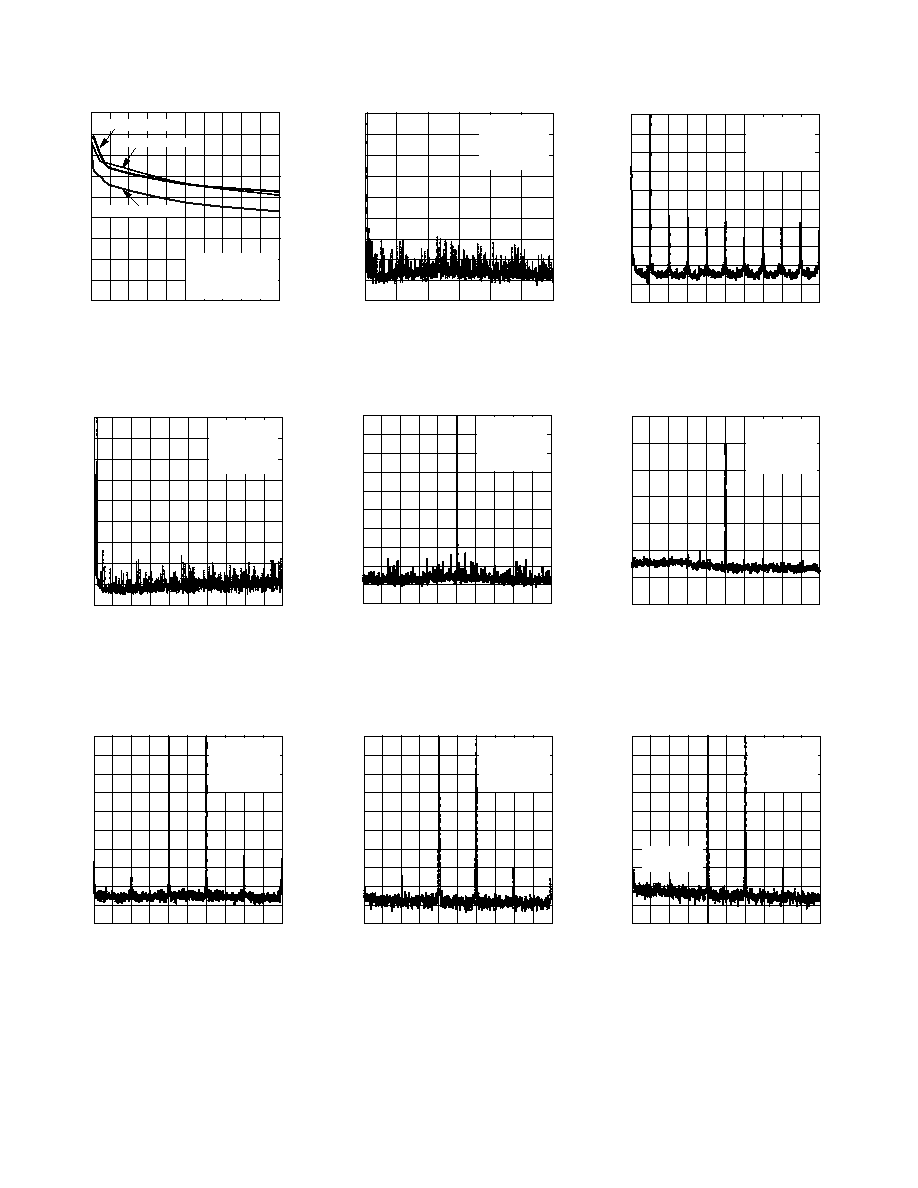
AD5424/AD5433/AD5445
11
0
2
4
6
8
10
12
14
1
10
100
1k
10k 100k 1M
10M 100M
FREQUENCY (Hz)
I
DD
(mA)
T
A
= 25 C
LOADING ZS TO FS
V
DD
= 5V
V
DD
= 3V
V
DD
= 2.5V
TPC 19. Supply Current vs.
Update Rate
9
6
3
0
3
10k
100k
1M
10M
100M
FREQUENCY (Hz)
T
A
= 25 C
V
DD
= 5V
AD5445
V
REF
= 2V, AD8038 C
C
1.47pF
V
REF
= 2V, AD8038 C
C
1pF
V
REF
= 0.15V, AD8038 C
C
1pF
V
REF
= 0.15V, AD8038 C
C
1.47pF
V
REF
= 3.51V, AD8038 C
C
1.8pF
GAIN (dB)
TPC 22. Reference Multiplying
Bandwidth vs. Frequency and
Compensation Capacitor
120
100
80
60
0
20
1
10
100
1k
10k
100k
1M
10M
FREQUENCY (Hz)
40
20
T
A
= 25 C
V
DD
= 3V
AMP = AD8038
FULL SCALE
ZERO SCALE
PSRR (dB)
TPC 25. Power Supply
Rejection vs. Frequency
102
66
54
42
30
18
6
6
1
10
100
1k
10k 100k 1M
10M 100M
FREQUENCY (Hz)
GAIN (dB)
T
A
= 25 C
LOADING
ZS TO FS
0
60
48
36
24
12
84
72
78
90
96
T
A
= 25 C
V
DD
= 5V
V
REF
= 3.5V
INPUT
C
COMP
= 1.8pF
AD8038 AMPLIFIER
AD5445 DAC
ALL ON
DB11
DB10
DB9
DB8
DB7
DB6
DB5
DB4
DB3
DB2
DB1
DB0
ALL OFF
TPC 20. Reference Multiplying
Bandwidth vs. Frequency and
Code
0.010
0.005
0
0.005
0.010
0.015
0.020
0.025
0.030
0.035
0.040
0.045
OUTPUT VOLTAGE (V)
7FF TO 800H
V
DD
= 5V
V
DD
= 3V
V
DD
= 3V
800 TO 7FFH
0
200
TIME (ns)
T
A
= 25 C
V
REF
= 0V
AD8038 AMPLIFIER
C
COMP
= 1.8pF
20
40
60
80 100 120 140 160 180
V
DD
= 5V
TPC 23. Midscale Transition,
V
REF
= 0 V
90
85
80
65
60
1
10
100
1k
10k
100k
1M
FREQUENCY (Hz)
75
70
T
A
= 25 C
V
DD
= 3V
V
REF
= 3.5 V p-p
THD + N (dB)
TPC 26. THD and Noise vs.
Frequency
0.8
0.6
0.4
0.2
0
0.2
1
10
100
1k
10k 100k 1M
100M
FREQUENCY (Hz)
T
A
= 25 C
V
DD
= 5V
V
REF
= 3.5V
C
COMP
= 1.8pF
AD8038 AMPLIFIER
AD5445 DAC
10M
GAIN (dB)
TPC 21. Reference Multiplying
Bandwidth--All Ones Loaded
1.77
1.76
1.75
1.74
1.73
1.72
1.71
1.70
1.69
1.68
OUTPUT VOLTAGE (V)
7FF TO 800H
V
DD
= 5V
V
DD
= 3V
V
DD
= 3V
800 TO 7FFH
0
200
TIME (ns)
T
A
= 25 C
V
REF
= 3.5V
AD8038 AMPLIFIER
C
COMP
= 1.8pF
20
40
60
80 100 120 140 160 180
V
DD
= 5V
TPC 24. Midscale Transition,
V
REF
= 3.5 V
0
20
40
60
80
100
SFDR (dB)
0
200
f
OUT
(kHz)
T
A
= 25 C
V
REF
= 3.5V
AD8038 AMPLIFIER
AD5445
20
40
60
80 100 120 140 160 180
MCLK = 1MHz
MCLK = 0.5MHz
MCLK = 200kHz
TPC 27. Wideband SFDR vs.
f
OUT
Frequency
REV. 0
12
AD5424/AD5433/AD5445
0
20
40
60
80
SFDR (dB)
0
1000
f
OUT
(kHz)
T
A
= 25 C
V
REF
= 3.5V
AD8038 AMPLIFIER
AD5445
100 200 300 400 500 600 700 800 900
MCLK = 5MHz
MCLK = 10MHz
MCLK = 25MHz
10
30
50
70
90
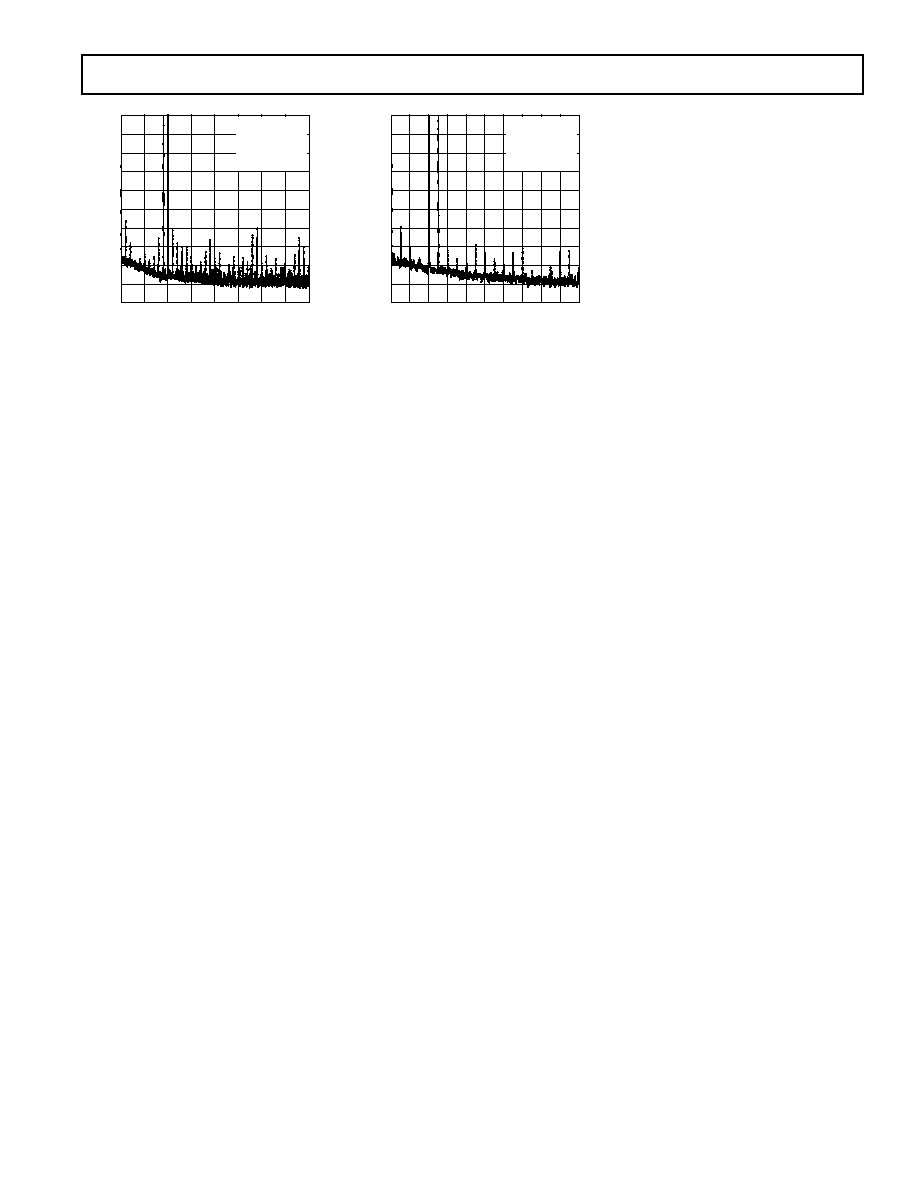
TPC 28. Wideband SFDR vs.
f
OUT
Frequency
SFDR (dB)
0
5.0
FREQUENCY (MHz)
0.5 1.0 1.5
4.0 4.5
2.0 2.5 3.0 3.5
90
70
50
30
10
80
60
40
20
0
T
A
= 25 C
V
DD
= 5V
AMP = AD8038
AD5445
65k CODES
TPC 31. Wideband SFDR,
f
OUT
= 50 kHz, Clock = 10 MHz
100
40
20
(dB)
200
700
FREQUENCY (MHz)
250 300 350
600 650
50
30
10
0
90
400 450 500 550
T
A
= 25 C
V
DD
= 3V
AMP = AD8038
AD5445
65k CODES
60
70
80
TPC 34. Narrow-Band IMD,
f
OUT
= 400 kHz, 500 kHz,
Clock = 10 MHz
90
70
50
30
10
SFDR (dB)
0
12
FREQUENCY (MHz)
2
4
6
8
10
80
60
40
20
0
T
A
= 25 C
V
DD
= 5V
AMP = AD8038
AD5445
65k CODES
TPC 29. Wideband SFDR,
f
OUT
= 100 kHz, Clock = 25 MHz
100
70
50
30
10
SFDR (dB)
250
750
FREQUENCY (kHz)
300 350 400
650 700
80
60
40
20
0
90
450 500 550 600
T
A
= 25 C
V
DD
= 3V
AMP = AD8038
AD5445
65k CODES
TPC 32. Narrow-Band Spectral
Response, f
OUT
= 500 kHz,
Clock = 25 MHz
100
40
20
(dB)
70
120
FREQUENCY (MHz)
75
80
85
110 115
50
30
10
0
90
90
95 100 105
T
A
= 25 C
V
DD
= 3V
AMP = AD8038
AD5445
65k CODES
60
70
80
TPC 35. Narrow-Band IMD,
f
OUT
= 90 kHz, 100 kHz,
Clock = 10 MHz
100
70
50
30
10
SFDR (dB)
0
5.0
FREQUENCY (MHz)
0.5 1.0 1.5
4.0 4.5
80
60
40
20
0
90
2.0 2.5 3.0 3.5
T
A
= 25 C
V
DD
= 5V
AMP = AD8038
AD5445
65k CODES
TPC 30. Wideband SFDR,
f
OUT
= 500 kHz, Clock = 10 MHz
120
60
20
SFDR (dB)
50
150
FREQUENCY (MHz)
60
70
80
130 140
80
40
0
20
100
90 100 110 120
T
A
= 25 C
V
DD
= 3V
AMP = AD8038
AD5445
65k CODES
TPC 33. Narrow-Band SFDR,
f
OUT
= 100 kHz, MCLK = 25 MHz
100
40
20
(dB)
20
70
FREQUENCY (MHz)
25
30
35
60
65
50
30
10
0
90
40
45
50
55
T
A
= 25 C
V
DD
= 5V
AMP = AD8038
AD5445
65k CODES
60
70
80
MCLK 10MHz
V
DD
5V
TPC 36. Narrow-Band IMD,
f
OUT
= 40 kHz, 50 kHz,
Clock = 10 MHz
REV. 0
AD5424/AD5433/AD5445
13
100
40
20
(dB)
0
400
FREQUENCY (kHz)
50
300
350
50
30
10
0
90
100
150
200
250
T
A
= 25 C
V
DD
= 5V
AMP = AD8038
AD5445
65k CODES
60
70
80
TPC 37. Wideband IMD, f
OUT
=
90 kHz, 100 kHz, Clock = 25 MHz
100
40
20
(dB)
0
200
FREQUENCY (kHz)
60
160 180
50
30
10
0
90
80 100 120 140
T
A
= 25 C
V
DD
= 5V
AMP = AD8038
AD5445
65k CODES
60
70
80
40
20
TPC 38. Wideband IMD, f
OUT
=
60 kHz, 50 kHz, Clock = 10 MHz

REV. 0
14
AD5424/AD5433/AD5445
TERMINOLOGY
Relative Accuracy
Relative accuracy or endpoint nonlinearity is a measure of the
maximum deviation from a straight line passing through the
endpoints of the DAC transfer function. It is measured after
adjusting for 0 and full scale and is normally expressed in LSBs
or as a percentage of full-scale reading.
Differential Nonlinearity
Differential nonlinearity is the difference between the measured
change and the ideal 1 LSB change between any two adjacent
codes. A specified differential nonlinearity of 1 LSB max over
the operating temperature range ensures monotonicity.
Gain Error
Gain error or full-scale error is a measure of the output error
between an ideal DAC and the actual device output. For these
DACs, ideal maximum output is V
REF
1 LSB. Gain error of
the DACs is adjustable to 0 with external resistance.
Output Leakage Current
Output leakage current is current that flows in the DAC ladder
switches when these are turned off. For the I
OUT
1 terminal, it
can be measured by loading all 0s to the DAC and measuring
the I
OUT
1 current. Minimum current will flow in the I
OUT
2 line
when the DAC is loaded with all 1s.
Output Capacitance
Capacitance from I
OUT
1 or I
OUT
2 to AGND.
Output Current Settling Time
This is the amount of time it takes for the output to settle to a
specified level for a full scale input change. For these devices, it
is specified with a 100
resistor to ground.
The settling time specification includes the digital delay from
CS rising edge to the full-scale output change.
Digital to Analog Glitch lmpulse
The amount of charge injected from the digital inputs to the
analog output when the inputs change state. This is normally
specified as the area of the glitch in either pA-secs or nV-secs
depending upon whether the glitch is measured as a current or
voltage signal.
Digital Feedthrough
When the device is not selected, high frequency logic activity on
the device digital inputs may be capacitively coupled through the
device to show up as noise on the I
OUT
pins and subsequently
into the following circuitry. This noise is digital feedthrough.
Multiplying Feedthrough Error
This is the error due to capacitive feedthrough from the DAC
reference input to the DAC I
OUT
1 terminal, when all 0s are
loaded to the DAC.
Total Harmonic Distortion (THD)
The DAC is driven by an ac reference. The ratio of the rms
sum of the harmonics of the DAC output to the fundamental
value is the THD. Usually only the lower order harmonics are
included, such as second to fifth.
THD
V
V
V
V
V
=
+
+
+
(
)
20
2
2
3
2
4
2
5
2
1
log
Digital Intermodulation Distortion
Second-order intermodulation distortion (IMD) measurements
are the relative magnitude of the fa and fb tones generated digi-
tally by the DAC and the second-order products at 2fa fb and
2fb fa.
Spurious-Free Dynamic Range (SFDR)
It is the usable dynamic range of a DAC before spurious noise
interferes or distorts the fundamental signal. SFDR is the mea-
sure of difference in amplitude between the fundamental and
the largest harmonically or nonharmonically related spur from
dc to full Nyquist bandwidth (half the DAC sampling rate, or
f
S
/2). Narrow band SFDR is a measure of SFDR over an arbi-
trary window size, in this case 50% of the fundamental. Digital
SFDR is a measure of the usable dynamic range of the DAC
when the signal is digitally generated sine wave.
REV. 0
AD5424/AD5433/AD5445
15
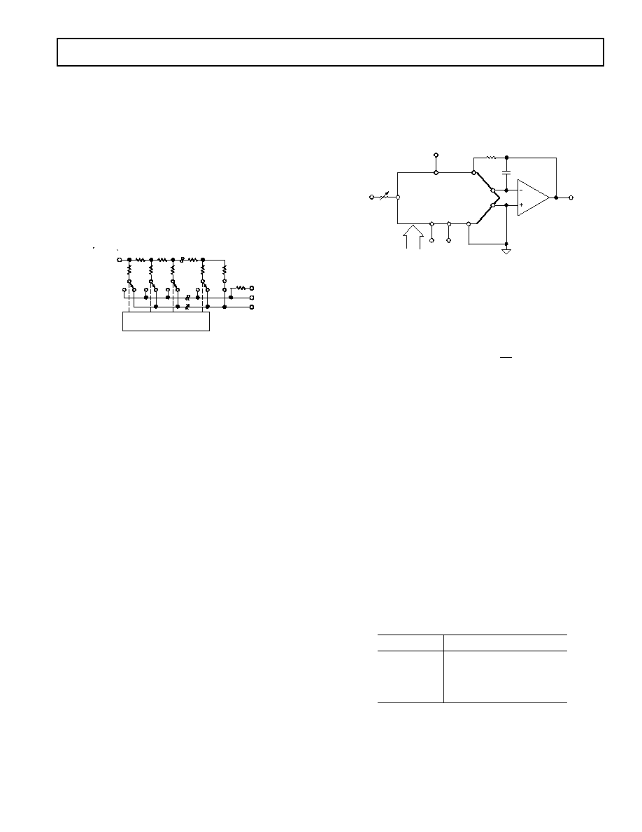
DAC SECTION
The AD5424, AD5433, and AD5445 are 8-, 10- and 12-bit
current output DACs consisting of a standard inverting R-2R
ladder configuration. A simplified diagram for the 8-bit AD5424
is shown in Figure 3. The matching feedback resistor R
FB
has a
value of R. The value of R is typically 10 k
(minimum 8 k
and maximum 12 k
). If I
OUT
1 and I
OUT
2
are kept at the same
potential, a constant current flows in each ladder leg, regardless
of digital input code. Therefore, the input resistance presented
at V
REF
is always constant and nominally of resistance value R.
The DAC output (I
OUT
) is code-dependent, producing various
resistances and capacitances. External amplifier choice should
take into account the variation in impedance generated by the
DAC on the amplifiers inverting input node.
V
REF
I
OUT
2
DAC DATA LATCHES
AND DRIVERS
2R
S1
2R
S2
2R
S3
2R
S8
2R
R
R
R
I
OUT
1
R
FB
A
R
Figure 3. Simplified Ladder
Access is provided to the V
REF
, R
FB
, I
OUT
1 and I
OUT
2 terminals
of the DAC, making the device extremely versatile and allowing it
to be configured in several different operating modes, for example,
to provide a unipolar output, 4-quadrant multiplication in bipo-
lar mode or in single-supply modes of operation. Note that a
matching switch is used in series with the internal R
FB
feedback
resistor. If users attempt to measure R
FB
, power must be applied
to V
DD
to achieve continuity.
PARALLEL INTERFACE
Data is loaded to the AD5424/33/45 in the format of an 8-, 10-, or
12-bit parallel word. Control lines
CS and R/W allow data to be
written to or read from the DAC register. A write event takes place
when
CS and R/W are brought low, data available on the data
lines fills the shift register, and the rising edge of
CS latches the
data and transfers the latched data-word to the DAC register.
The DAC latches are not transparent, thus a write sequence must
consist of a falling and rising edge on
CS to ensure data is loaded
to the DAC register and its analog equivalent reflected on the
DAC output.
A read event takes place when R/
W is held high and CS is brought
low. Now data is loaded from the DAC register back to the input
register and out onto the data line where it can be read back to
the controller for verification or diagnostic purposes.
CIRCUIT OPERATION
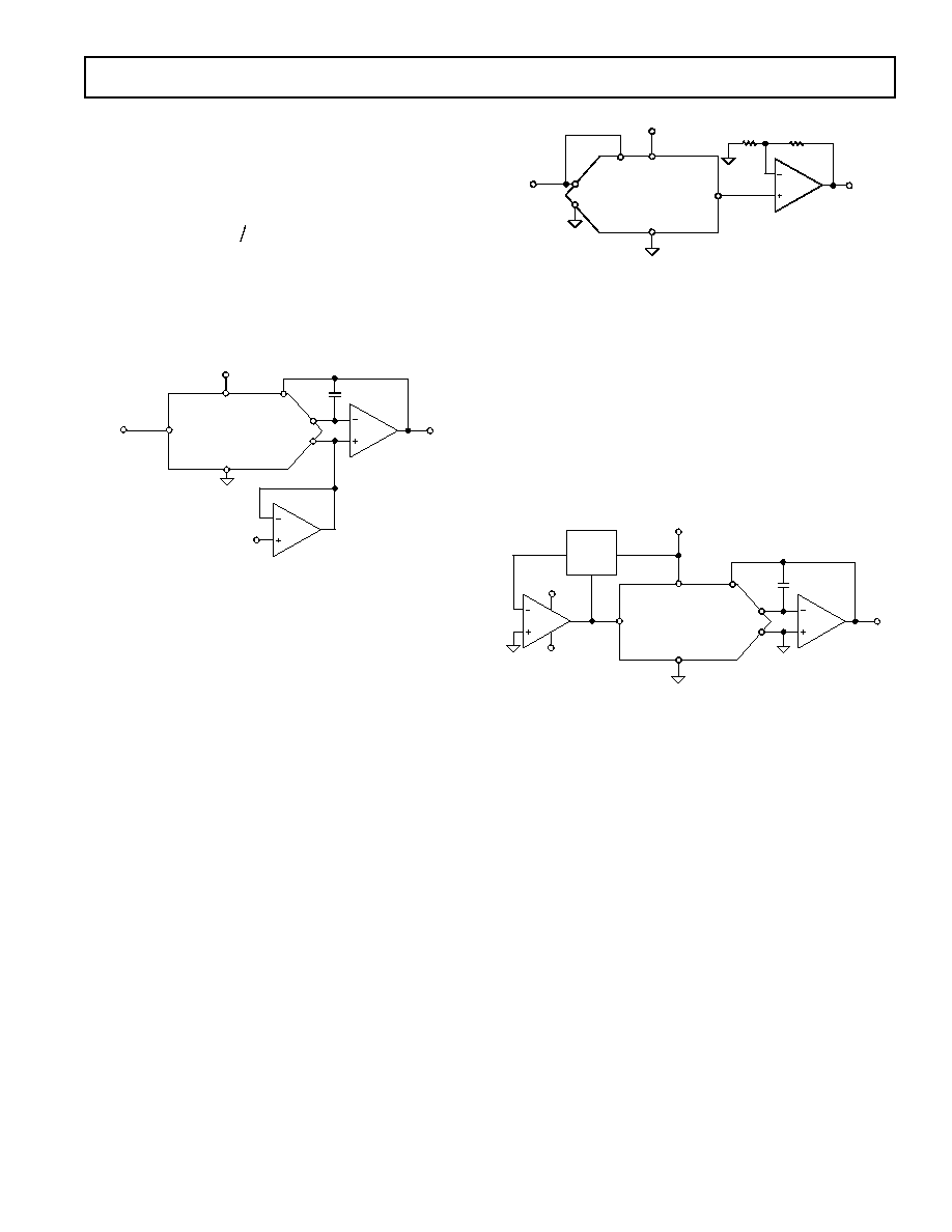
Unipolar Mode
Using a single op amp, these devices can easily be configured to
provide 2-quadrant multiplying operation or a unipolar output
voltage swing as shown in Figure 4.
V
OUT
=
0 TO V
REF
GND
V
REF
I
OUT
2
I
OUT
1
R
FB
AGND
AD5424/
AD5433/AD5445
NOTES
1. R1 AND R2 USED ONLY IF GAIN ADJUSTMENT IS REQUIRED.
2. C1 PHASE COMPENSATION (1pF 2pF) MAY BE REQUIRED
IF A1 IS A HIGH SPEED AMPLIFIER.
R1
R2
A1
V
REF
V
DD
V
DD
C1
CS
R/
W
DATA
INPUTS
Figure 4. Unipolar Operation
When an output amplifier is connected in unipolar mode, the
output voltage is given by
V
V
OUT
REF
=
×
D
n
2
where D is the fractional representation of the digital word loaded
to the DAC and n is the resolution of the DAC.
D = 0 to 255 (8-Bit AD5424)
= 0 to 1023 (10-Bit AD5433)
= 0 to 4095 (12-Bit AD5445)
Note that the output voltage polarity is opposite to the V
REF
polarity for dc reference voltages.
These DACs are designed to operate with either negative or
positive reference voltages. The V
DD
power pin is only used
by the internal digital logic to drive the DAC switches' on
and off states.
These DACs are also designed to accommodate ac reference
input signals in the range of 10 V to +10 V.
With a fixed 10 V reference, the circuit shown in Figure 4 will
give a unipolar 0 V to 10 V output voltage swing. When V
IN
is
an ac signal, the circuit performs 2-quadrant multiplication.
Table I shows the relationship between digital code and expected
output voltage for unipolar operation. (AD5424, 8-bit device).
Table I. Unipolar Code Table
Digital Input
Analog Output (V)
1111 1111
V
REF
(255/256)
1000 0000
V
REF
(128/256) = V
REF
/2
0000 0001
V
REF
(1/256)
0000 0000
V
REF
(0/256) = 0
REV. 0
16
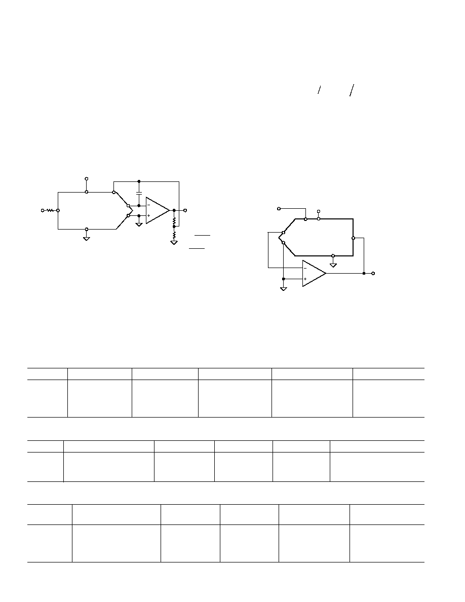
AD5424/AD5433/AD5445
V
OUT
= V
REF
TO +V
REF
GND
V
REF
10V
I
OUT
2
I
OUT
1
V
DD
V
REF
NOTES
1. R1 AND R2 ARE USED ONLY IF GAIN ADJUSTMENT IS REQUIRED.
ADJUST R1 FOR V
OUT
= 0 V WITH CODE 10000000 LOADED TO DAC.
2. MATCHING AND TRACKING IS ESSENTIAL FOR RESISTOR PAIRS R3 AND R4.
3. C1 PHASE COMPENSATION (1pF2pF) MAY BE REQUIRED IF A1/A2 IS
A HIGH SPEED AMPLIFIER.
AGND
R3
10k
AD5424/
AD5433/AD5445
R5
20k
R4
10k
A2
R1
V
DD
R
FB
R2
C1
CS
R/
W
DATA
INPUTS
A1
Figure 5. Bipolar Operation (4-Quadrant Multiplication)
Bipolar Operation
In some applications, it may be necessary to generate full
4-quadrant multiplying operation or a bipolar output swing. This
can be easily accomplished by using another external amplifier and
some external resistors as shown in Figure 5. In this circuit, the
second amplifier A2 provides a gain of 2. Biasing the external
amplifier with an offset from the reference voltage results in full
4-quadrant multiplying operation. The transfer function of this
circuit shows that both negative and positive output voltages
are created as the input data (D) is incremented from code
zero (V
OUT
= V
REF
) to midscale (V
OUT
= 0 V ) to full scale
(V
OUT
= +V
REF
).
V
V
D
V
OUT
REF
n
REF
=
×
(
)
-
-
2
1
where D is the fractional representation of the digital word loaded
to the DAC and n is the resolution of the DAC.
D = 0 to 255 (8-Bit AD5424)
= 0 to 1023 (10-Bit AD5433)
= 0 to 4095 (12-Bit AD5445)
When V
IN
is an ac signal, the circuit performs 4-quadrant
multiplication.
Table II shows the relationship between digital code and the
expected output voltage for bipolar operation (AD5426, 8-bit
device).
Table II. Bipolar Code Table
Digital Input
Analog Output (V)
1111 1111
+V
REF
(127/128)
1000 0000
0
0000 0001
V
REF
(127/128)
0000 0000
V
REF
(128/128)
Stability
In the I-to-V configuration, the I
OUT
of the DAC and the invert-
ing node of the op amp must be connected as close as possible,
and proper PCB layout techniques must be employed. Since
every code change corresponds to a step function, gain peaking
may occur if the op amp has limited GBP and there is excessive
parasitic capacitance at the inverting node. This parasitic capaci-
tance introduces a pole into the open-loop response, which can
cause ringing or instability in closed-loop applications.
An optional compensation capacitor, C1, can be added in parallel
with R
FB
for stability as shown in Figures 4 and 5. Too small a
value of C1 can produce ringing at the output, while too large
a value can adversely affect the settling time. C1 should be
found empirically but 1 pF to 2 pF is generally adequate
for compensation.
REV. 0
AD5424/AD5433/AD5445
17
SINGLE-SUPPLY APPLICATIONS
Current Mode Operation
Figure 6 shows a typical circuit for operation with a single 2.5 V to
5 V supply. In the current mode circuit of Figure 6, I
OUT
2
and
hence I
OUT
1 is biased positive by the amount applied to V
BIAS
. In
this configuration, the output voltage is given by
V
D
R
R
V
V
V
OUT
FB
DAC
BIAS
IN
BIAS
=
×
(
)
×
-
(
)
{
}
+
As D varies from 0 to 255 (AD5424), 1023 (AD5433), or
4095 (AD5445), the output voltage varies from V
OUT
= V
BIAS
to V
OUT
= 2 V
BIAS
V
IN
.
V
BIAS
should be a low impedance source capable of sinking and
sourcing all possible variations in current at the I
OUT
2 terminal.
V
OUT
GND
V
IN
I
OUT
2
I
OUT
1
R
FB
V
DD
V
REF
V
BIAS
C1
NOTES
1. ADDITIONAL PINS OMITTED FOR CLARITY
2. C1 PHASE COMPENSATION (1pF2pF) MAY BE REQUIRED
IF A1 IS A HIGH SPEED AMPLIFIER.
V
DD
A1
DAC
Figure 6. Single-Supply Current Mode Operation
Voltage Switching Mode of Operation
Figure 7 shows these DACs operating in the voltage-switching
mode. The reference voltage, V
IN
, is applied to the I
OUT
1 pin;
I
OUT
2 is connected to AGND; and the output voltage is avail-
able at the V
REF
terminal. In this configuration, a positive
reference voltage results in a positive output voltage making
single-supply operation possible. The output from the DAC is
voltage at a constant impedance (the DAC ladder resistance),
thus an op amp is necessary to buffer the output voltage. The
reference input no longer sees a constant input impedance, but
one that varies with code. So, the voltage input should be driven
from a low impedance source.
It is important to note that V
IN
is limited to low voltages be-
cause the switches in the DAC ladder no longer have the same
source-drain drive voltage. As a result, their on resistance dif-
fers, which degrades the linearity of the DAC. See TPCs 1015.
Also, V
IN
must not go negative by more than 0.3 V or an inter-
nal diode will turn on, exceeding the max ratings of the device.
In this type of application, the full range of multiplying capabil-
ity of the DAC is lost.
V
OUT
V
DD
GND
V
IN
I
OUT
2
I
OUT
1
R
FB
V
DD
V
REF
NOTES
1. ADDITIONAL PINS OMITTED FOR CLARITY
2. C1 PHASE COMPENSATION (1pF 2pF) MAY BE REQUIRED
IF A1 IS A HIGH SPEED AMPLIFIER.
R2
R1
DAC
A1
Figure 7. Single-Supply Voltage Switching Mode Operation
POSITIVE OUTPUT VOLTAGE
Note that the output voltage polarity is opposite to the V
REF
polarity for dc reference voltages. In order to achieve a positive
voltage output, an applied negative reference to the input of the
DAC is preferred over the output inversion through an inverting
amplifier because of the resistor tolerance errors. To generate a
negative reference, the reference can be level shifted by an op
amp such that the V
OUT
and GND pins of the reference become
the virtual ground and 2.5 V respectively, as shown in Figure 8.
V
OUT
=
0 TO +2.5V
V
DD
= 5V
GND
I
OUT
2
I
OUT
1
R
FB
V
DD
V
REF
C1
NOTES
1. ADDITIONAL PINS OMITTED FOR CLARITY
2. C1 PHASE COMPENSATION (1pF2pF) MAY BE REQUIRED
IF A1 IS A HIGH SPEED AMPLIFIER.
GND
V
IN
V
OUT
ADR03
+5V
5V
1/2 AD8552
1/2 AD8552
2.5V
8-/10-/12-BIT DAC
Figure 8. Positive Voltage Output with Minimum
of Components
REV. 0
18
AD5424/AD5433/AD5445
ADDING GAIN
In applications where the output voltage is required to be greater
than V
IN
, gain can be added with an additional external amplifier or
it can also be achieved in a single stage. It is important to consider
the effect of temperature coefficients of the thin film resistors of
the DAC. Simply placing a resistor in series with the RFB resistor
will cause mismatches in the temperature coefficients resulting in
larger gain temperature coefficient errors. Instead, the circuit of
Figure 9 is a recommended method of increasing the gain of the
circuit. R1, R2, and R3 should all have similar temperature coef-
ficients, but they need not match the temperature coefficients of the
DAC. This approach is recommended in circuits where gains of
great than 1 are required.
V
OUT
V
DD
GND
I
OUT
2
I
OUT
1
R
FB
V
DD
V
REF
C1
NOTES
1. ADDITIONAL PINS OMITTED FOR CLARITY
2. C1 PHASE COMPENSATION (1pF 2pF) MAY BE
REQUIRED IF A1 IS A HIGH SPEED AMPLIFIER.
R3
R2
R1
V
IN
R1 = R2R3
R2 + R3
GAIN = R2 + R3
R2
8-/10-/12-BIT DAC
Figure 9. Increasing Gain of Current Output DAC
USING DACS AS A DIVIDER OR A PROGRAMMABLE
GAIN ELEMENT
Current steering DACs are very flexible and lend themselves to
many different applications. If this type of DAC is connected as
the feedback element of an op amp and R
FB
is used as the input
resistor as shown in Figure 10, then the output voltage is inversely
proportional to the digital input fraction D. For D = 1 2
n
the
output voltage is
V
V
D
V
OUT
IN
IN
n
= -
= -
-
(
)
-
1 2
As D is reduced, the output voltage increases. For small values
of the digital fraction D, it is important to ensure that the
amplifier does not saturate and also that the required accuracy
is met. For example, an 8-bit DAC driven with the binary code
10H (00010000), i.e., 16 decimal, in the circuit of Figure 10
should cause the output voltage to be 16 V
IN
. However, if the
DAC has a linearity specification of
±0.5 LSB then D can in
fact have the weight anywhere in the range 15.5/256 to 16.5/256
so that the possible output voltage will be in the range 15.5 V
IN
to
16.5 V
IN
--an error of +3% even though the DAC itself has a
maximum error of 0.2%.
V
OUT
V
DD
GND
V
IN
I
OUT
2
I
OUT
1
R
FB
V
DD
V
REF
NOTE
ADDITIONAL PINS OMITTED FOR CLARITY
Figure 10. Current Steering DAC Used as a Divider
or Programmable Gain Element
Table III. Suitable ADI Precision References Recommended for Use with AD5424/AD5433/AD5445 DACs
Part No.
Output Voltage
Initial Tolerance
Temperature Drift
0.1 Hz to 10 Hz Noise
Package
ADR01
10 V
0.1%
3 ppm/
°C
20 V p-p
SC70, TSOT, SOIC
ADR02
5 V
0.1%
3 ppm/
°C
10 V p-p
SC70, TSOT, SOIC
ADR03
2.5 V
0.2%
3 ppm/
°C
10 V p-p
SC70, TSOT, SOIC
ADR425
5 V
0.04%
3 ppm/
°C
3.4 V p-p
MSOP, SOIC
Table IV. Some Precision ADI Op Amps Suitable for Use with AD5424/AD5433/AD5445 DACs
Part No.
Max Supply Voltage (V)
V
OS
(max) ( V)
I
B
(max) (nA)
GBP (MHz)
Slew Rate (V/ s)
OP97
±20
25
0.1
0.9
0.2
OP1177
±18
60
2
1.3
0.7
AD8551
±6
5
0.05
1.5
0.4
Table V. Some High Speed ADI Op Amps Suitable for Use with AD5424/AD5433/AD5445 DACs
Max Supply Voltage
BW @ A
CL
Slew Rate
V
OS
(max)
I
B
(max)
Part No.
(V)
(MHz)
(V/ s)
( V)
(nA)
AD8065
±12
145
180
1500
0.01
AD8021
±12
200
100
1000
1000
AD8038
±5
350
425
3000
0.75
AD9631
±5
320
1300
10000
7000

REV. 0
AD5424/AD5433/AD5445
19
DAC leakage current is also a potential error source in divider
circuits. The leakage current must be counterbalanced by an
opposite current supplied from the op amp through the DAC.
Since only a fraction D of the current into the V
REF
terminal is
routed to the I
OUT
1 terminal, the output voltage has to change
as follows:
Output Error Voltage Due to DAC Leakage = (Leakage R)/D
where R is the DAC resistance at the V
REF
terminal. For a DAC
leakage current of 10 nA, R = 10 k
and a gain (i.e., 1/D) of 16
the error voltage is 1.6 mV.
REFERENCE SELECTION
When selecting a reference for use with the AD5424 series of
current output DACs, pay attention to the references output
voltage temperature coefficient specification. This parameter not
only affects the full-scale error, but can also affect the linearity
(INL and DNL) performance. The reference temperature coeffi-
cient should be consistent with the system accuracy specifications.
For example, an 8-bit system required to hold its overall specifi-
cation to within 1 LSB over the temperature range 0 C to 50 C
dictates that the maximum system drift with temperature should
be less than 78 ppm/ C. A 12-bit system with the same tempera-
ture range to overall specification within 2 LSBs requires a
maximum drift of 10 ppm/ C. By choosing a precision reference
with low output temperature coefficient this error source can be
minimized. Table III suggests some references available from
Analog Devices that are suitable for use with this range of cur-
rent output DACs.
AMPLIFIER SELECTION
The primary requirement for the current-steering mode is an
amplifier with low input bias currents and low input offset voltage.
The input offset voltage of an op amp is multiplied by the vari-
able gain (due to the code dependent output resistance of the
DAC) of the circuit. A change in this noise gain between two
adjacent digital fractions produces a step change in the output
voltage due to the amplifier's input offset voltage. This output
voltage change is superimposed on the desired change in output
between the two codes and gives rise to a differential linearity error,
which if large enough, could cause the DAC to be nonmonotonic.
In general, the input offset voltage should be <1/4 LSB to ensure
monotonic behavior when stepping through codes.
The input bias current of an op amp also generates an offset at
the voltage output as a result of the bias current flowing in the
feedback resistor RFB. Most op amps have input bias currents
low enough to prevent any significant errors in 12-bit applications.
Common-mode rejection of the op amp is important in voltage
switching circuits since it produces a code dependent error at the
voltage output of the circuit. Most op amps have adequate common
mode rejection for use at 8-, 10-, and 12-bit resolution.
Provided the DAC switches are driven from true wideband
low impedance sources (V
IN
and AGND), they settle quickly.
Consequently, the slew rate and settling time of a voltage switching
DAC circuit is determined largely by the output op amp. To
obtain minimum settling time in this configuration, it is important
to minimize capacitance at the V
REF
node (voltage output node
in this application) of the DAC. This is done by using low
inputs capacitance buffer amplifiers and careful board design.
Most single-supply circuits include ground as part of the analog
signal range, which in turns requires an amplifier that can handle
rail-to-rail signals; there is a large range of single-supply amplifiers
available from Analog Devices.
PCB LAYOUT AND POWER SUPPLY DECOUPLING
In any circuit where accuracy is important, careful consideration
of the power supply and ground return layout helps to ensure
the rated performance. The printed circuit board on which the
AD5424/AD5433/AD5445 is mounted should be designed so
that the analog and digital sections are separated, and confined
to certain areas of the board. If the DAC is in a system where
multiple devices require an AGND-to-DGND connection, the
connection should be made at one point only. The star ground
point should be established as close as possible to the device.
These DACs should have ample supply bypassing of 10 F in
parallel with 0.1 F on the supply located as close to the package
as possible, ideally right up against the device. The 0.1 F capaci-
tor should have low effective series resistance (ESR) and effective
series inductance (ESI), like the common ceramic types that
provide a low impedance path to ground at high frequencies, to
handle transient currents due to internal logic switching. Low
ESR 1 F to 10 F tantalum or electrolytic capacitors should
also be applied at the supplies to minimize transient disturbance
and filter out low frequency ripple.
Fast switching signals such as clocks should be shielded with
digital ground to avoid radiating noise to other parts of the board,
and should never be run near the reference inputs.
Avoid crossover of digital and analog signals. Traces on opposite
sides of the board should run at right angles to each other. This
reduces the effects of feedthrough through the board. A micros-
trip technique is by far the best, but not always possible with a
double-sided board. In this technique, the component side of
the board is dedicated to ground plane, while signal traces are
placed on the solder side.
It is good practice to employ compact, minimum lead length
PCB layout design. Leads to the input should be as short as
possible to minimize IR drops and stray inductance.
The PCB metal traces between V
REF
and R
FB
should also be
matched to minimize gain error. To maximize on high frequency
performance, the I-to-V amplifier should be located as close to
the device as possible.
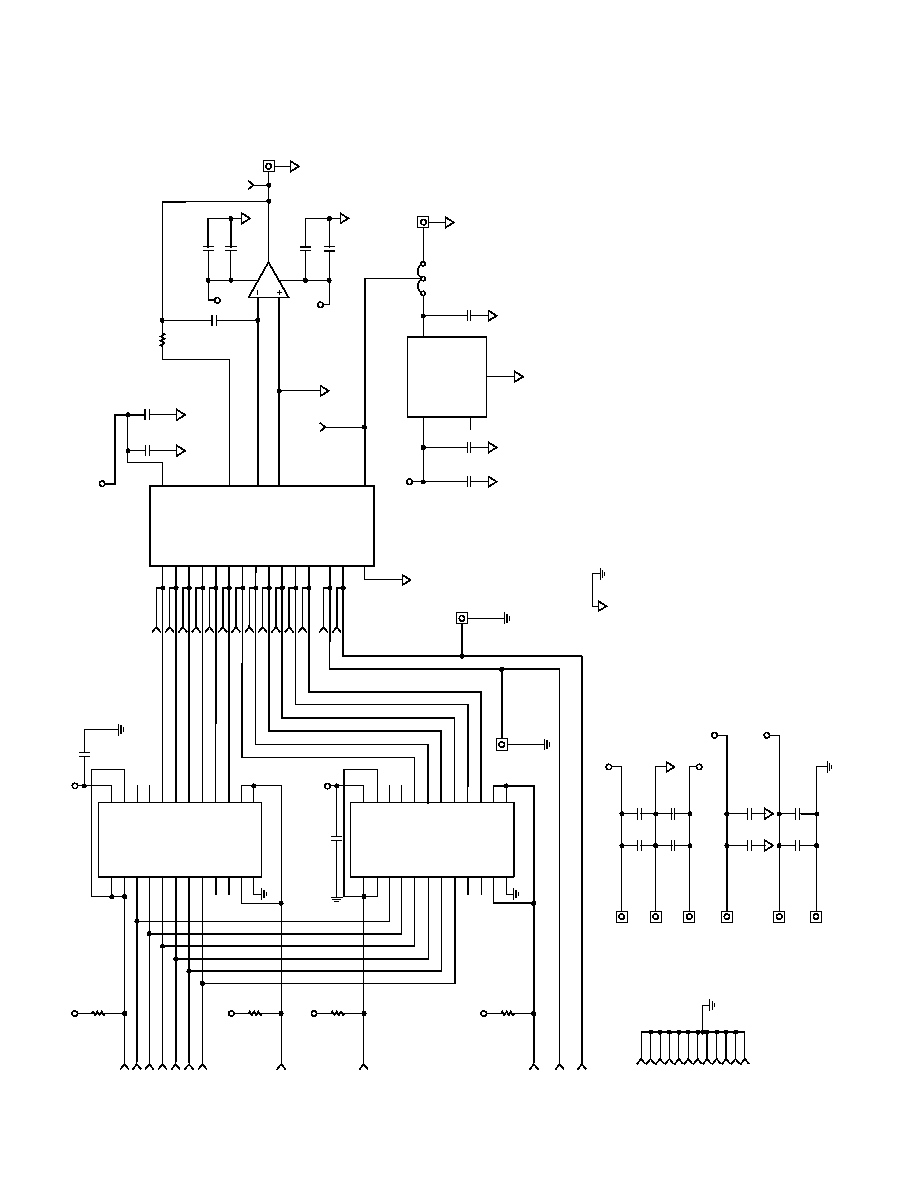
EVALUATION BOARD FOR THE AD5424/AD5433/AD5445
The board consists of a 12-bit AD5445 and a current to voltage
amplifier AD8065. Included on the evaluation board is a 10 V
reference ADR01. An external reference may also be applied via
an SMB input.
The evaluation kit consists of a CD-ROM with self-installing
PC software to control the DAC. The software simply allows
the user to write a code to the device.
OPERATING THE EVALUATION BOARD
Power Supplies
The board requires
±12 V, and +5 V supplies. The +12 V V
DD
and V
SS
are used to power the output amplifier, while the +5 V
is used to power the DAC (V
DD1
) and transceivers (V
CC
).
Both supplies are decoupled to their respective ground plane
with 10 F tantalum and 0.1 F ceramic capacitors.
Link1 (LK1) is provided to allow selection between the on-board
reference (ADR01) or an external reference applied through J2.
REV. 0
20
AD5424/AD5433/AD5445
V
DD
V
SS
I
OUT
2
V
DD
R
FB
V
REF
TP2
V
DD
+V
IN
V
OUT
TRIM
GND
I
OUT
1
AD5424/AD5433/
AD5445
U1
U3
LK1
C8
0.1
F
C7
4.7pF
C9
10
F
C10
0.1
F
C3
10
F
C4
0.1
F
P119
P120
P121
P122
P123
P124
P125
P126
P127
P128
P129
P130
P23
P22
P21
P24
AG
N
D
V
SS
V
DD
1
V
DD
C13
0.1
F
C14
10
F
C15
0.1
F
C16
10
F
C17
0.1
F
C18
10
F
+
P26
P25
C19
0.1
F
C20
10
F
+
+
+
U2
ADR01AR
4
5
2
6
J1
7
4
3
2
6
V
V+
+
C11
10
F
C12
0.1
F
+
TP1
R1
V
DD
1
C5
10
F
C6
0.1
F
+
DB0
15
DB1
14
DB7
8
DB8
7
DB9
6
DB10
5
DB11
4
CS
16
RW
17
DB6
9
DB5
10
DB4
11
DB3
12
DB2
13
3
A
B
17
18
13
14
22
21
20
19
23
23
15
16
5
6
12
11
10
9
8
7
2
1
3
4
B5
B4
OEAB
LEAB
B0
B1
B2
B3
CEBA
B7
B6
A2
A3
GND
CEAB
A7
A6
A5
A4
OEBA
LEBA
A0
A1
5
6
12
11
10
9
8
7
2
1
3
4
B5
B4
OEAB
LEAB
B0
B1
B2
B3
CEBA
B7
B6
A2
A3
GND
CEAB
A7
A6
A5
A4
OEBA
LEBA
A0
A1
R2
10k
V
CC
R3
10k
V
CC
R4
10k
V
CC
R5
10k
V
CC
V
CC
VCC
V
CC
VCC
P136
P131
P18
P11
P114
P17
P16
P15
P14
P13
P12
P19
AB (MSB)
BA (MSB)
AB (LSB)
BA (LSB)
J4
J3
J2
EXTERNAL
REFERENCE
OUTPUT
C2
0.1
F
C1
0.1
F
U5
U4
74ABT543
74ABT543
V
CC
17
18
13
14
22
21
20
19
23
24
15
16
GND
DB0
DB1
DB7
DB8
DB9
DB10
DB11
CS
R/
W
DB6
DB5
DB4
DB3
DB2
18
20
1
2
19
Figure 11. Evaluation Board Schematic
REV. 0
AD5424/AD5433/AD5445
21
EVAL-AD5424/
AD5433/AD5445EB
J1
OUTPUT
EXT
VREF
R/W
DB10
DB8
DB6
DB4
DB2
DB0
DB11
DB9
DB7
DB5
DB3
DB1
U1
U3
C4
C3
U2
J2
CS
RW
R3
J4
U4
C20
C19
C17
C18
C14
C16
C13
C15
P2
CS
J3
P1
R2
C1
C2
C12
C5
C8
C7
LK1
TP1
C6
R1
C10
TP2
R4
R5
U5
VCC
DGND
A
GND
VSS
VDD
VDD1
Figure 12. Silkscreen--Component Side View

REV. 0
22
AD5424/AD5433/AD5445
Table VI. Bill of Materials for AD5424/AD5433/AD5445 Evaluation Board
Name
Part Description
Value
Tolerance
PCB Decal
Stock Code
C1, C2, C4,
C6, C8
X7R Ceramic Capacitor
0.1 F
10%
0603
FEC 499-675
C10, C12, C13,
C15
X7R Ceramic Capacitor
0.1 F
10%
0603
FEC 499-675
C3, C5, C9,
C11, C14
Tantalum Capacitor Taj Series
10 F 20 V
10%
CAP\TAJ_B
FEC 197-427
C17, C19
X7R Ceramic Capacitor
0.1 F
10%
0603
FEC 499-675
C16, C18, C20
Tantalum Capacitor Taj Series
10 F 10 V
10%
CAP\TAJ_A
FEC 197-130
C7
X7R Ceramic Capacitor
4.7 pF
10%
0603
CS
TESTPOINT
TESTPOINT
FEC 240-345 (Pack)
DB0DB11
Red Testpoint
TESTPOINT
FEC 240-345 (Pack)
J1J4
SMB Socket
SMB
FEC 310-682
LK1
3-Pin Header (3 1)
LINK-3P-
FEC 511-717 and 150-411
P1
36-Pin Centronics Connector
36WAY
FEC 147-753
P2
6-Pin Terminal Block
CON\POWER6
FEC 151-792
R1
0.063 W Resistor
0603
Not Inserted
R2, R3, R4, R5
0.063 W Resistor
10 k
1%
0603
FEC 911-355
RW, TP1, TP2
Red Testpoint
TESTPOINT
FEC 240-345 (Pack)
U1
AD5445
TSSOP20
AD5445BRU
U2
*
ADR425/ADR01/ADR02/ADR03
SO8NB
ADR01AR
U3
*
AD8065
SO8NB
AD8065AR
U4
74ABT543
TSSOP24
Fairchild 74ABT543CMTC
U5
74ABT543
TSSOP24
Fairchild 74ABT543CMTC
Each Corner
Rubber Stick-on Feet
FEC 148-922
*See section on Amplifier and Reference Selection
FEC - Farnell Electronic Components, Units 4 and 5 Gofton Court, Jamestown Road, Finglas, Dublin 11, Ireland. Tel. Int +353 (0)1 8309277
www.farnell.com

REV. 0
AD5424/AD5433/AD5445
23
Overview of AD54xx Devices
Part No.
Resolution
No. DACs
INL
t
S
max
Interface
Package
Features
AD5403
*
8
2
±0.25 60 ns
Parallel
CP-40
10 MHz Bandwidth,
10 ns
CS Pulse Width,
4-Quadrant Multiplying Resistors
AD5410
*
8
1
±0.25 100 ns
Serial
RU-16
10 MHz Bandwidth, 50 MHz Serial,
4-Quadrant Multiplying Resistors
AD5413
*
8
2
±0.25 100 ns
Serial
RU-24
10 MHz Bandwidth, 50 MHz Serial,
4-Quadrant Multiplying Resistors
AD5424
8
1
±0.25 60 ns
Parallel
RU-16, CP-20 10 MHz Bandwidth,
17 ns
CS Pulse Width
AD5425
8
1
±0.25 100 ns
Serial
RM-10
Byte Load, 10 MHz Bandwidth,
50 MHz Serial
AD5426
8
1
±0.25 100 ns
Serial
RM-10
10 MHz Bandwidth, 50 MHz Serial
AD5428
8
2
±0.25 60 ns
Parallel
RU-20
10 MHz Bandwidth,
17 ns
CS Pulse Width
AD5429
8
2
±0.25 100 ns
Serial
RU-10
10 MHz Bandwidth, 50 MHz Serial
AD5450
8
1
±0.25 100 ns
Serial
RJ-8
10 MHz Bandwidth, 50 MHz Serial
AD5404
*
10
2
±0.5
70 ns
Parallel
CP-40
10 MHz Bandwidth,
17 ns
CS Pulse Width,
4-Quadrant Multiplying Resistors
AD5411
*
10
1
±0.5
110 ns
Serial
RU-16
10 MHz Bandwidth, 50 MHz Serial,
4-Quadrant Multiplying Resistors
AD5414
*
10
2
±0.5
110 ns
Serial
RU-24
10 MHz Bandwidth, 50 MHz Serial,
4-Quadrant Multiplying Resistors
AD5432
10
1
±0.5
110 ns
Serial
RM-10
10 MHz Bandwidth, 50 MHz Serial
AD5433
10
1
±0.5
70 ns
Parallel
RU-20, CP-20 10 MHz Bandwidth,
17 ns
CS Pulse Width
AD5439
10
2
±0.5
110 ns
Serial
RU-16
10 MHz Bandwidth, 50 MHz Serial
AD5440
10
2
±0.5
70 ns
Parallel
RU-24
10 MHz Bandwidth,
17 ns
CS Pulse Width
AD5451
10
1
±0.25 110 ns
Serial
RJ-8
10 MHz Bandwidth, 50 MHz Serial
AD5405
12
2
±1
120 ns
Parallel
CP-40
10 MHz Bandwidth,
17 ns
CS Pulse Width,
4-Quadrant Multiplying Resistors
AD5412*
12
1
±1
160 ns
Serial
RU-16
10 MHz Bandwidth, 50 MHz Serial,
4-Quadrant Multiplying Resistors
AD5415
12
2
±1
160 ns
Serial
RU-24
10 MHz Bandwidth, 50 MHz Serial,
4-Quadrant Multiplying Resistors
AD5443
12
1
±1
160 ns
Serial
RM-10
10 MHz Bandwidth, 50 MHz Serial
AD5445
12
1
±1
120 ns
Parallel
RU-20, CP-20 10 MHz Bandwidth,
17 ns
CS Pulse Width
AD5447
12
2
±1
120 ns
Parallel
RU-24
10 MHz Bandwidth,
17 ns
CS Pulse Width
AD5449
12
2
±1
160 ns
Serial
RU-16
10 MHz Bandwidth,
17 ns
CS Pulse Width
AD5452
12
1
±0.5
160 ns
Serial
RJ-8, RM-8
10 MHz Bandwidth, 50 MHz Serial
AD5453
14
1
±2
180 ns
Serial
RJ-8, RM-8
10 MHz Bandwidth, 50 MHz Serial
*Future parts, contact factory for availability
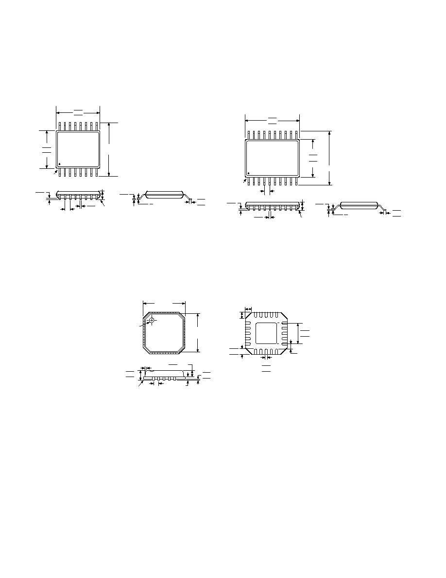
REV. 0
C03160010/03(0)
24
AD5424/AD5433/AD5445
OUTLINE DIMENSIONS
20-Lead Lead Frame Chip Scale Package [LFCSP]
(CP-20)
Dimensions shown in millimeters
1
20
5
6
11
16
15
BOTTOM
VIEW
10
2.25
2.10 SQ
1.95
0.75
0.55
0.35
0.30
0.23
0.18
0.50
BSC
12
MAX
0.20
REF
0.80 MAX
0.65 NOM
0.05
0.02
0.00
1.00
0.90
0.80
SEATING
PLANE
PIN 1
INDICATOR
TOP
VIEW
3.75
BSC SQ
4.0
BSC SQ
COPLANARITY
0.08
0.60
MAX
0.60
MAX
0.25 MIN
COMPLIANT TO JEDEC STANDARDS MO-220-VGGD-1
20-Lead Thin Shrink Small Outline Package [TSSOP]
(RU-20)
Dimensions shown in millimeters
20
1
11
10
6.40 BSC
4.50
4.40
4.30
PIN 1
6.60
6.50
6.40
SEATING
PLANE
0.15
0.05
0.30
0.19
0.65
BSC
1.20
MAX
0.20
0.09
0.75
0.60
0.45
8
0
COMPLIANT TO JEDEC STANDARDS MO-153AC
COPLANARITY
0.10
16-Lead Thin Shrink Small Outline Package [TSSOP]
(RU-16)
Dimensions shown in millimeters
16
9
8
1
PIN 1
SEATING
PLANE
8
0
4.50
4.40
4.30
6.40
BSC
5.10
5.00
4.90
0.65
BSC
0.15
0.05
1.20
MAX
0.20
0.09
0.75
0.60
0.45
0.30
0.19
COPLANARITY
0.10
COMPLIANT TO JEDEC STANDARDS MO-153AB
Document Outline
- FEATURES
- APPLICATIONS
- GENERAL DESCRIPTION
- FUNCTIONAL BLOCK DIAGRAM
- SPECIFICATIONS
- TIMING CHARACTERISTICS
- ABSOLUTE MAXIMUM RATINGS
- ORDERING GUIDE
- PIN CONFIGURATIONS
- AD5424 PIN FUNCTION DESCRIPTIONS
- PIN CONFIGURATIONS
- AD5433 PIN FUNCTION DESCRIPTIONS
- PIN CONFIGURATIONS
- AD5445 PIN FUNCTION DESCRIPTIONS
- Typical Performance Characteristics
- TERMINOLOGY
- Relative Accuracy
- Differential Nonlinearity
- Gain Error
- Output Leakage Current
- Output Capacitance
- Output Current Settling Time
- Digital to Analog Glitch lmpulse
- Digital Feedthrough
- Multiplying Feedthrough Error
- Total Harmonic Distortion (THD)
- Digital Intermodulation Distortion
- Spurious-Free Dynamic Range (SFDR)
- DAC SECTION
- PARALLEL INTERFACE
- CIRCUIT OPERATION
- Unipolar Mode
- Bipolar Operation
- Stability
- SINGLE-SUPPLY APPLICATIONS
- Current Mode Operation
- Voltage Switching Mode of Operation
- POSITIVE OUTPUT VOLTAGE
- ADDING GAIN
- USING DACS AS A DIVIDER OR APROGRAMMABLE GAIN ELEMENT
- REFERENCE SELECTION
- AMPLIFIER SELECTION
- PCB LAYOUT AND POWER SUPPLY DECOUPLING
- EVALUATION BOARD FOR THE AD5424/AD5433/AD5445
- OPERATING THE EVALUATION BOARD
- Overview of AD54xx Devices
- OUTLINE DIMENSIONS